WD1035DH
Http//:www.sh-willsemi.com
WD1035DH
High Efficiency 5V, 3A continuous, 1.5MHz
Synchronous Step-Down Regulator
Descriptions
WD1035DH is a high efficiency 1.5MHz synchronous
step-Down DC/DC regulator capable of delivering up
to 3A output current. It can operate over a wide input
voltage range from 2.7V to 5.5V and integrate main
switch and synchronous switch with very low RDSON to
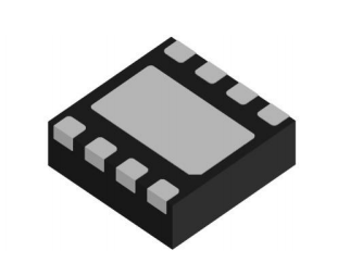
DFN2x2-8L Package
minimize the conduction loss.
WD1035DH also provides over temperature protection
(OTP), under-voltage lockout (UVLO), VOUT short
protection.
The WD1035DH is available in the DFN2x2-8L
package.
Standard
product
is
Pb-Free
and
FB
1
PG
2
IN
3
Exposed
Pad
PGND 4
Halogen-Free.
8
SGND
7
EN
6
LX
5
NC
Pin configuration (Top view)
Features
⚫
Low Rdson
internal Switches (top/bottom):
100/60mΩ
⚫
2.7-5.5V input voltage range
⚫
3A continuous load current capability
⚫
1.5MHz
switching
frequency
minimizes
1035
DHYW
the
external components
⚫
45uA low quiescent current
⚫
Internal soft-start limits the inrush current
⚫
Constant On Time (COT) Control for fast transient
response
⚫
100% Duty-Cycle Mode
⚫
Power-Good Output
Smart Phones
⚫
TV
⚫
Set Top Box and OTT box
⚫
Access Point Router
Will Semiconductor Ltd.
= Device Code
DH
= Special code
Y
= Year Code
W
= Week Code
Marking
Applications
⚫
1035
Order information
1
Device
Package
Shipping
WD1035DH-8/TR
DFN2x2-8L
3000/Reel&Tape
2018.03 - Rev. 1.0.2
�WD1035DH
Typical Applications
L1:1uH
Vin:2.7-5.5V
Cin
10uF
IN
LX
R1
C1
120K 22pF
WD1035DH
EN
ON/OFF
100K
FB
Cout
22uF
R2
60K
PG
PGND SGND
Fig1 Schematic Diagram
Pin Descriptions
Pin Name
Pin Number
FB
1
Pin Description
Feedback pin. Connected to the feedback resistor for adjustable
version or VOUT for fix output version.
Power good indicator. The output of this pin is an open-drain with
PG
2
external pull-up resistor. PG is pulled up when the FB voltage is within
90%, otherwise it is LOW.
IN
3
Input pin. Decouple this pin to GND with at least 10uF ceramic Cap.
PGND
4
Power Ground.
NC
5
No Internal Connection.
LX
6
Inductor pin.
EN
7
Enable Control. Pull high to turn on. Do not leave it floating .
SGND
8
Signal Ground.
Exposed Pad
Will Semiconductor Ltd.
The exposed pad must be soldered to a large PCB and connected to
PGND for maximum power dissipation.
2
2018.03 - Rev. 1.0.2
�WD1035DH
Absolute Maximum Ratings (1)
Parameter
MIN
MAX
Unit
Power Supply VCC
-0.3
6.5
V
Others Pins
-0.3
VCC+0.6
V
2.19
W
Package Thermal Resistance TJA
50
°C /W
Package Thermal Resistance TJC
8
°C /W
Junction Temperature TJ
150
°C
Lead Temperature (Soldering,10 sec)
260
°C
150
°C
Power Dissipation, PD @ TA =25℃,DFN2X2-8L
Storage Temperature Range
ESD Ratings
(1)
-65
HBM
2000
V
CDM
2000
V
Stresses beyond those listed under "absolute maximum ratings" may cause permanent damage to the device. These
are stress ratings only and functional operation of the device at these or any other conditions beyond those indicated
under "recommended operating conditions" is not implied. Exposure to absolute-maximum-rated conditions for
extended periods may affect device reliability.
Recommended Operating Conditions
Parameter
MIN
MAX
Unit
Power Supply VCC
2.7
5.5
V
Junction temperature TJ
-40
125
°C
Ambient temperature TA
-40
85
°C
Will Semiconductor Ltd.
3
2018.03 - Rev. 1.0.2
�WD1035DH
Electronics Characteristics
Unless otherwise specified: limits for typical values are for TA = 25℃ and minimum and maximum limits apply over the
operating ambient temperature range (-40℃ < TA < 85℃); VIN=4.2V,Vout=2.5V,L1=1uH,Cout=22uF.
Parameter
Symbol
Operation Voltage Range
VIN
Test Conditions
Min
Typ
2.7
Max
Unit
5.5
V
VUVLO-H
VIN Rising
2.45
V
VUVLO-L
VIN Falling
2.25
V
Quiescent Current
IQ
Switching
45
uA
Shutdown Current
ISD
VEN =GND, VIN =3.6V
Feedback Reference
VREF
Line Regulation
ΔVOUT /ΔVIN
0.35
PFET Rdson
Rdson P
100
NFET Rdson
Rdson N
60
PFET Current Limit
ILIMT
4.5
A
Oscillator Frequency
FOSC
1.5
MHz
Max Duty Cycle
100
%
Soft Start Time
800
uS
Power on delay time
25
uS
6.3
V
6
V
20
uS
150
°C
30
°C
VIN Under Voltage Lockout
Input OVP shutdown
VOVP
0.588
Rising
Falling
5.6
Over Volatage Protection
Blanking Time
Thermal Shutdown
Thermal Shutdown
Hysteresis
EN Input LOW Voltage
VIL
EN Input HIGH Voltage
VIH
Will Semiconductor Ltd.
0.6
1
μA
0.612
V
%/V
mΩ
0.4
1.4
4
V
V
2018.03 - Rev. 1.0.2
�WD1035DH
Typical Characteristics
100
100
90
90
80
80
70
70
Efficieny(%)
Efficieny(%)
(Ta=25oC, VIN=5V, VEN=VIN, CIN=10μF ,COUT=22μF, L1=1μH, unless otherwise noted)
60
50
40
30
10
0
500
1000
1500
2000
2500
50
40
30
VIN=2.7V
VIN=3.6V
VIN=5.5V
VOUT=1.8V,L=1uH
20
60
VIN=2.7V
VIN=3.6V
VIN=5.5V
VOUT=0.6V,L=1uH
20
10
0
3000
0
500
Load Current (mA)
Efficieny vs.Load Current
0.615
1.82
0.610
Output Voltage (V)
Output Voltage (V)
2000
2500
3000
0.605
1.81
1.80
1.79
1.78
1.77
1.76
1.75
VIN=2.7V
VIN=3.6V
VIN=5.5V
VOUT=1.8V,L=1uH
1.74
1.73
0
500
0.600
0.595
0.590
0.585
0.580
0.575
0.570
VIN=2.7V
VIN=3.6V
VIN=5.5V
VOUT=0.6V,L=1uH
0.565
0.560
0.555
1000
1500
2000
2500
0.550
3000
0
Output Current (mA)
Output Voltage vs.Output Current
1.80
1.85
1.79
1.84
1.78
1.83
1.77
1.76
1.75
1.74
1.73
1.72
1.71
1.70
-50
VIN=2.7V
VIN=3.6V
VIN=5.5V
VOUT=1.8V,L=1uH
IOUT=2A
-25
0
1000
1500
2000
25
50
75
100
2500
3000
1.82
1.81
1.80
1.79
VIN=2.7V
VIN=3.6V
VIN=5.5V
VOUT=1.8V,L=1uH
IOUT=1mA
1.78
1.77
1.76
1.75
-50
125
-25
0
25
50
75
100
125
Temperature (،)و
Output Voltage vs.Temperature
Temperature (،)و
Output Voltage vs.Temperature
Will Semiconductor Ltd.
500
Output Current (mA)
Output Voltage vs.Output Current
Output Voltage (V)
Output Voltage (V)
1500
Load Current (mA)
Efficieny vs.Load Current
1.83
1.72
1000
5
2018.03 - Rev. 1.0.2
�WD1035DH
0.14
55
0.12
Shutdown Current(uA)
60
IQ(uA)
50
45
40
35
EN=VIN
L=1uH,VO=1.8V
30
2.5
3.0
3.5
4.0
4.5
5.0
0.10
0.08
0.06
0.04
0.02
0.00
2.5
5.5
Input Voltage (V)
Supply Current vs. Input Voltage
3.5
4.0
4.5
5.0
5.5
Oscillator Frequency(MHz)
1.66
1.60
Frequency (MHz)
3.0
Input Voltage (V)
Shutdown Current vs. Input Voltage
1.62
1.58
1.56
1.54
1.52
L=1uH,VO=1.8V
VIN=3.6V,IOUT=1000mA
1.50
-50
EN=0V
L=1uH
VOUT=1.8V
-25
0
25
50
75
100
1.62
1.60
1.58
1.56
1.54
1.52
1.50
1.48
1.46
2.5
125
Temperature (،)و
Frequency vs. Temperature
Will Semiconductor Ltd.
1.64
IO=1000mA
L=1uH,VO=1.8V
3.0
3.5
4.0
4.5
5.0
5.5
Input Voltage (V)
Oscillator Frequency VS. Input Voltage
6
2018.03 - Rev. 1.0.2
�WD1035DH
VIN=3.6V, VO=1.8V,EN=3.6V , IO=2A, EN On
VIN=3.6V, VO=1.8V,EN=3.6V , IO=1A, EN Off
Load Transient Response
Load Transient Response
VIN=5V,VO=1.8V,EN=3.6V,IO=1mA-2A
Ripple : VIN=5.0V, VO=0.6V,EN=3.6V
Will Semiconductor Ltd.
IO=1A
VIN=5V,VO=0.6V,EN=5V,IO=1mA-2A
Ripple : VIN=5.0V, VO=0.6V,EN=3.6V
7
IO=2A
2018.03 - Rev. 1.0.2
�WD1035DH
Ripple : VIN=5.0V, VO=1.8V,EN=3.6V
VIN=3.6V, VO=1.8V,EN=3.6V
Will Semiconductor Ltd.
IO=1A
Ripple : VIN=5.0V, VO=1.8V,EN=3.6V
IO=2A
VOUT short
8
2018.03 - Rev. 1.0.2
�WD1035DH
Operation Information
WD1035DH
is
synchronous
a
high
efficiency
1.5MHz
ripple current. It is suggested to choose the ripple
Step-Down DC/DC regulator IC
current to be about 40% of the maximum output
capable of delivering up to 3A output current. It can
current. The inductance is calculated as:
operate over a wide input voltage range from 2.7V
L=
to 5.5V and integrate main switch and synchronous
switch with very low RDSON
to minimize the
conduction loss.
Application Information
Because of the high integration in the WD1035DH
IC, the application circuit based on this regulator IC
is rather simple. Only input capacitor Cin, output
Where Fsw is the switching frequency and Iout,max
is the maximum load current.
2) The saturation current rating of the inductor must
be selected to be greater than the peak inductor
current under full load conditions.
ISAT,MIN > IOUT,MAX +
capacitor Cout, output inductor L and feedback
resistors (RH and RL) need to be selected for the
targeted applications specifications.
Feedback resistor dividers RH and RL :
Choose RH and RL to program the proper output
voltage. To minimize the power consumption under
light loads, it is desirable to choose larger resistance
values for both RH and RL. A value of between
100kΩ and 1MΩ is highly recommended for both
resistors. If RL =120kΩ is chosen, then RH can be
calculated to be:
(Vout − 0.6V) ∗ R L
RH =
0.6V
VOUT (1 − Vout /VIN,MAX )
FSW × IOUT,MAX×40%
VOUT (1 − Vout /VIN,MAX )
2 ∗ FSW ∗ L
3) The DCR of the inductor and the core loss at the
switching frequency must be low enough to achieve
the desired efficiency requirement. It is desirable to
choose an inductor with DCR


 工商网监
湘ICP备2023018690号
工商网监
湘ICP备2023018690号
