Techcode®
DATASHEET
TD1432
2A 150KHz PWM Buck DC/DC Converter
General Description
Features
TD1432 is a monolithic asynchronous buck regulator. The
device provides 2A of continuous load current over a wide
input voltage of 9V to 40V. It uses current mode control to
regulator the output voltage and provides fast transient
response.
Requiring a minimum number of external components, these
regulators are simple to use and include internal frequency
compensation, and a fixed-frequency oscillator. Anti-ring
function is to reduce the influence of EMI.
This device, available in a SOP-8 package, provides a very
compact system solution with minimal reliance on external
components.
⚫
⚫
⚫
⚫
⚫
⚫
⚫
⚫
⚫
Internal Power MOSFET
2A continuous output current
Up to 90% efficiency
Input voltage range: 9V to 40V
Fixed 150kHz frequency internal oscillator
Current limit protection
Anti-ringing for lower EMI
Over temperature protection
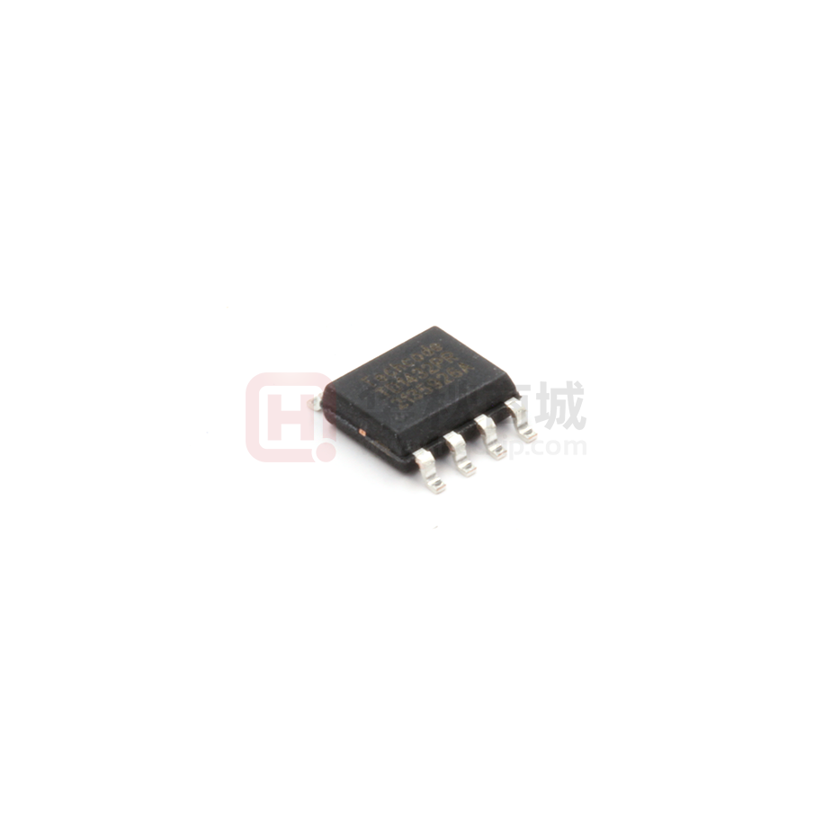
SOP-8 package
Applications
⚫
⚫
⚫
⚫
⚫
Simple high-efficiency step-down regulator
Efficient pre-regulator for linear regulators
On-card switching regulators
Positive to negative converter
Battery charger
Pin Configurations
VIN
1
SW
2
FB
ON/OFF
8
GND
7
GND
3
6
GND
4
5
GND
TD1432
Figure1 Pin Configuration of TD1432(Top View)
April 1, 2022.
Techcode Semiconductor Limited
1
www.techcodesemi.com
�Techcode®
DATASHEET
TD1432
2A 150KHz PWM Buck DC/DC Converter
Pin Description
Pin Number
Pin Name
Description
1
VIN
Power Input. In supplies the power to the IC, as well as the step-down converter
switches. Drive IN with a 9V to 40V power source. Bypass IN to GND with a suitably
large capacitor to eliminate noise on the input to the IC. See Input Capacitor.
2
SW
Power Switching Output. SW is the switching node that supplies power to the output.
Connect the output LC filter from SW to the output load.
3
FB
Feedback Input. FB senses the output voltage to regulate that voltage. Drive FB with a
resistive voltage divider from the output voltage. The feedback threshold is 1.23V.
4
ON/OFF
Enable Input. ON/OFF is a digital input that turns the regulator on or off. Diver ON/OFF
low to turn on the regulator; drive it high to turn it off. Do not floating when Vin>32V.
GND
Ground.
5,6,7,8
Ordering Information
TD1432
□
□
Circuit Type
Output voltage:
5: 5V
R: ADJ
Package
P: SOP8
April 1, 2022.
Techcode Semiconductor Limited
2
www.techcodesemi.com
�Techcode®
DATASHEET
TD1432
2A 150KHz PWM Buck DC/DC Converter
Function Block
VIN
ON/OFF
Start up
&
Regulator
Current
Sense
LDO
Current
Limit
comp
UVLO
Power
MOS
Bandgap
Control
Logic&
Driver
Buffer
OSC
FB
Vs
Vref1
EA
SW
PWM
comp
Vcomp
Anti-ringing
Circuit
R1
C1
EA
Clamp
Softstart
Thermal
Shutdown
Short Circuit
Protection
Over Voltage
Protection
AGND
Figure 2 Function Block Diagram of TD1432
Absolute Maximum Ratings
Parameter
Input Voltage
Feedback Pin Voltage
ON/OFF Pin Voltage
Output Pin Voltage
Power Dissipation
Operating Junction Temperature
Storage Temperature
Lead Temperature
ESD (HBM)
MSL
Thermal Resistance-Junction to Ambient
Thermal Resistance-Junction to Case
April 1, 2022.
symbol
VIN
VFB
VEN
VSW
PD
TJ
TSTG
TLEAD
RθJA
RθJC
Techcode Semiconductor Limited
3
Value
-0.3 to 42
-0.3 to 5
-0.3 to 5
-0.3 to VIN+0.3
Internally limited
150
-65 to 150
260
2000
Level3
85
45
Unit
V
V
V
V
mW
℃
℃
℃
V
℃/W
℃/W
www.techcodesemi.com
�Techcode®
DATASHEET
TD1432
2A 150KHz PWM Buck DC/DC Converter
Recommended Operating Conditions
Parameter
Input voltage
Output voltage
Converter output current
Operating junction temperature
Operating ambient temperature
Symbol
VIN
Vout
Iout
TJ
TA
Min.
9
1.23
0
-40
-40
Max.
40
Unit
V
V
A
℃
℃
2
125
85
Electrical Characteristics
VIN =12V, TA =+25℃, unless otherwise noted
Parameter
Symbol
Condition
Min
Typ
Max
Units
TD1432PR
VFB
9V≤VIN≤40V
1.200
1.23
1.26
V
TD1432P5
VOUT
9V≤VIN≤40V
ON/OFF=5V
4.8
5.0
5.2
V
-
-
10
uA
IQ
ON/OFF=0V; VFB=1.5V
-
3
4.5
mA
FOSC1
VFB>0.3
120
150
180
kHz
-
400
-
mΩ
-
3.8
-
A
-
-
98
%
Shutdown Supply Current
Quiescent current
Oscillation Frequency
Highside Switch On Resistance
Current Limit
Maximum Duty Cycle
ON/OFF Threshold voltage
RDS(ON)
IL
Peak output current
DMAX
VIL
Low(Regulator ON)
-
0.9
-
V
VIH
High(Regulator OFF)
-
1.0
-
V
VIN Rising
-
8.3
-
V
Input Under Voltage Lockout Threshold
Hysteresis
-
500
-
mV
Thermal Shutdown
-
160
-
℃
Input Under Voltage Lockout Threshold
April 1, 2022.
Techcode Semiconductor Limited
4
www.techcodesemi.com
�Techcode®
DATASHEET
TD1432
2A 150KHz PWM Buck DC/DC Converter
Typical Application Circuit
CFF
R1 3.6K
R2 11K
3
FB
47uH
1
DC
IN
Vin
TD1432PR
SW
Cin1 220uf
Cin2 0.1uf
GND
5-8
5V
2
Cout 330uf
D1
ON/OFF
4
SK34
DC
LOAD
Figure 3 Typical Application of TD1432PR
3
FB
47uH
1
DC
IN
Vin
TD1432P5
SW
Cin1 220uf
Cin2 0.1uf
GND
5-8
5V
2
ON/OFF
4
D1
SK34
Cout 330uf
DC
LOAD
Figure 4 Typical Application of TD1432P5
April 1, 2022.
Techcode Semiconductor Limited
5
www.techcodesemi.com
�Techcode®
DATASHEET
TD1432
2A 150KHz PWM Buck DC/DC Converter
Function Description
The TD1432 regulates input voltages from 9V to 40V down
to an output voltage as low as 1.23V, and supplies up to 2A
of load current.
The TD1432 uses current-mode control to regulate the
output voltage. The output voltage is measured at FB
through a resistive voltage divider and amplified through the
internal trans-conductance error amplifier. The output
voltage of the error amplifier is compared to the switch
current (measured internally) to control the output voltage.
Setting the Output Voltage
The output voltage is set using a resistive voltage divider
connected from the output voltage to FB. The voltage
divider divides the output voltage down to the feedback
voltage by the ratio:
R1
VFB = VOUT × (
)
R1 + R 2
Thus the output voltage is:
VOUT = 1.23 × (
where ILOAD is the load current.
The choice of which style inductor to use mainly depends on
the price vs. size requirements and any EMI constraints.
Input Capacitor
The input current to the step-down converter is
discontinuous, therefore a capacitor is required to supply
the AC current while maintaining the DC input voltage. Use
low ESR capacitors for the best performance. Ceramic
capacitors are preferred, but tantalum or low-ESR
electrolytic capacitors will also suffice. Choose X5R or X7R
dielectrics when using ceramic capacitors. Since the input
capacitor (C1) absorbs the input switching current, it
requires and adequate ripple current rating. The RMS
current in the input capacitor can be estimated by:
R1 + R 2
)
R1
VOUT
VOUT
IC1 = ILOAD × √
× (1 −
)
VIN
VIN
Inductor
The inductor is required to supply constant current to the
load while being driven by the switched input voltage. A
larger value inductor will result in less ripple current that will
in turn result in lower output ripple voltage. However, the
larger value inductor will have a larger physical size, higher
series resistance, and/or lower saturation current. A good
rule for determining inductance is to allow the peak-to-peak
ripple current to be approximately 30% or the maximum
switch current limit. Also, make sure that the peak inductor
current is below the maximum switch current limit.
The inductance value can be calculated by:
VOUT
VOUT
L=
× (1 −
)
fS × ∆IL
VIN
Where VOUT is the output voltage, VIN is the input voltage, fs
is the switching frequency, and ∆IL is the peak-to-peak
inductor ripple current.
Choose an inductor that will not saturate under the
April 1, 2022.
maximum inductor peak current, calculated by:
VOUT
VOUT
LP = ILOAD +
× (1 −
)
2 × fS × L
VIN
The worst-case condition occurs at VIN=2VOUT, where IC1 =
ILOAD/2. For simplification, use an input capacitor with a RMS
current rating greater than half of the maximum load
current. The input capacitor can be electrolytic, tantalum or
ceramic. When using electrolytic or tantalum capacitor, be
placed as close to the IC as possible. When using ceramic
capacitors, make sure that they have enough capacitance to
provide sufficient charge to prevent excessive voltage ripple
at input. The input voltage ripple for low ESR capacitors can
be estimated by:
ILOAD VOUT
VOUT
∆VIN =
×
(1 −
)
C1 × fs
VIN
VIN
where C1 is the input capacitance Value.
Output Capacitor
The output capacitor (C2) is required to maintain the DC
output voltage. Ceramic, tantalum, or low ESR electrolytic
capacitors are recommended. Under typical application
Techcode Semiconductor Limited
6
www.techcodesemi.com
�Techcode®
DATASHEET
2A 150KHz PWM Buck DC/DC Converter
TD1432
conditions, a minimum ceramic capacitor value of 20µF is
recommended on the output. Low ESR capacitors are
preferred to keep the output voltage ripple low. The output
voltage ripple can be estimated by:
∆VOUT =
Vout
Vout
1
) × (R ESR +
)
× (1fs ×L
Vin
8×fS ×C2
Where C2 is the output capacitance value and RESR is the
equivalent series resistance (ESR) value of the output
capacitor.
When using ceramic capacitors, the impedance at the
switching frequency is dominated by the capacitance which
is the main cause for the output voltage ripple. For
simplification, the output voltage ripple can be estimated
by:
VOUT
VOUT
∆VOUT =
× (1 −
)
2
8 × fs × L × C2
VIN
When using tantalum or electrolytic capacitors. The ESR
dominates the impedance at the switching frequency. For
simplification, the output ripple can be approximated to:
VOUT
VOUT
∆VOUT =
× (1 −
) × R ESR
fs × L
VIN
The characteristics of the output capacitor also affect the
stability of the regulation system. The TD1432 can be
optimized for a wide range of capacitance and ESR values.
PCB Layout Guide
1. Input MLCC capacitor should be connected to the VIN pin
and the GND pin as close as possible.
2. Keep sensitive signal traces such as trace connecting FB
pin away from the VOUT pins
3. Make the current trace from SW pin to inductor to the
GND as short as possible.
4. Pour a maximized copper area to the GNDs pin and the
VIN pin to help thermal dissipation
。
April 1, 2022.
Techcode Semiconductor Limited
7
www.techcodesemi.com
�Techcode®
DATASHEET
2A 150KHz PWM Buck DC/DC Converter
TD1432
Package Information
SOP-8 Package Outline Dimensions
April 1, 2022.
Techcode Semiconductor Limited
8
www.techcodesemi.com
�Techcode®
DATASHEET
2A 150KHz PWM Buck DC/DC Converter
TD1432
Design Notes
April 1, 2022.
Techcode Semiconductor Limited
9
www.techcodesemi.com
�
很抱歉,暂时无法提供与“TD1432PR”相匹配的价格&库存,您可以联系我们找货
免费人工找货- 国内价格
- 1+1.55380
- 10+1.25896
- 30+1.13260
- 100+0.97492
- 500+0.90472
- 1000+0.81108
- 国内价格
- 1+0.94250
- 30+0.91000
- 100+0.84500
- 500+0.78000
- 1000+0.74750


 工商网监
湘ICP备2023018690号
工商网监
湘ICP备2023018690号
