LTC8721, LTC8722, LTC8723
P-1
General Description
The LTC8721/LTC8722/LTC8723 are tiny, single- and dual- channel comparators with
push-pull output that offer the ultimate combination of high speed (66 ns propagation
delay) and very low power consumption (22 μA), available in extremely small packages
with features such as rail-to-rail inputs, low offset voltage (0.8 mV), large output drive
current, and a wide range of supply voltages from 1.7 V to 5.5 V. The devices are very easy
to implement in a wide variety of applications where require critical response time,
power-sensitive, low-voltage, and/or tight board space.
The output of the LTC8721/LTC8722/LTC8723 pulls to within 0.1 V of either supply rail
without external pull-up circuitry, making these devices ideal for interface with both
CMOS and TTL logics. All input and output pins can tolerate a continuous short-circuit
fault condition to either rail. Internal hysteresis ensures clean output switching, even with
slow-moving input signals.
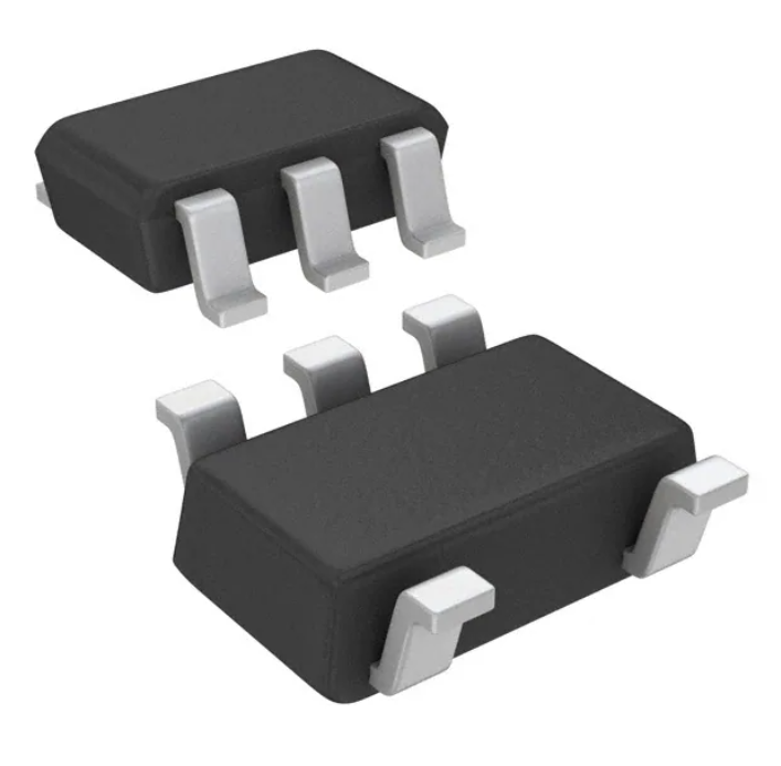
The LTC8721/LTC8723 (single) is available in both SOT23-5L and SC70-5L packages. The
LTC8722 (dual) is offered in DFN-8L, SOIC-8L and MSOP-8L packages. All devices are
rated over −40 ℃ to +125 ℃ industrial temperature range.
Features and Benefits
Micro-power Operating Current (22 μA) Preserves Battery Power
Fast 66 ns Propagation Delay (100-mV Overdrive)
Single 1.7 V to 5.5 V Supply Voltage Range
– Can be Powered From the Same 1.8V/2.5V/3.3V/5V System Rails
Rail-to-Rail Input
Push-Pull Output Current Drive: 30 mA Typically at 5V Supply
Internal Hysteresis for Clean Switching
Internal RF/EMI Filter
Operating Temperature Range: −40 ℃ to +125 ℃
Applications
Consumer Accessories
Handsets, Tablets and Notebooks
Portable and Battery-Powered Devices
Threshold Detectors and Discriminators
Alarms and Monitoring Circuits
Zero-Crossing Detectors
Window Comparators
Level Translators
Line Receivers
IR Receivers
Pin Configurations (Top View)
LTC8721
LTC8722
LTC8722
LTC8723
LTC8723R
SOT23-5L / SC70-5L
DFN-8L
SOIC-8L / MSOP-8L
SOT23-5L
SOT23-5L
OUT 1
5 +VS
–VS 2
+IN 3
4 –IN
OUTA 1
8 +VS
–INA 2
7 OUTB
OUT A
1
+INA 3
6 –INB
–IN A
2
–VS 4
5 +INB
+IN A
3
–VS
4
8
A
B
+VS
7
OUT B
6
–IN B
5
+IN B
CAUTION: These devices are sensitive to electrostatic discharge; follow proper IC Handling Procedures.
Linearin and designs are registered trademarks of Linearin Technology Corporation.
© Copyright Linearin Technology Corporation. All Rights Reserved.
All other trademarks mentioned are the property of their respective owners.
+IN 1
5 +VS
–VS 2
–IN 3
–IN 1
5 +VS
–VS 2
4 OUT
+IN 3
4 OUT
FN1617-37.1a — Data Sheet
Micro-Power 22μA, 66ns, 1.7V, RRI, CMOS Input Comparators
�LTC8721, LTC8722, LTC8723
P-2
Pin Description
Symbol
Description
–IN
Negative input. The voltage range is from (VS– – 0.1V) to (VS+ + 0.1V).
+IN
Positive input. This pin has the same voltage range as –IN.
+VS
Positive power supply. The voltage is from 1.7V to 5.5V. Split supplies are possible as
long as the voltage between VS+ and VS– is from 1.7V to 5.5V.
–VS
Negative power supply. It is normally tied to ground. It can also be tied to a voltage
other than ground as long as the voltage between VS+ and VS– is from 1.7V to 5.5V.
OUT
Comparator output.
Ordering Information
Orderable
Type Number
Package
Name
Package
Quantity
Eco Class(1)
Operating
Temperature
Marking
Code
LTC8721YT5/R6
SOT23-5L
3 000
Green
–40℃ to +125℃
CG1
LTC8721YC5/R6
SC70-5L
3 000
Green
–40℃ to +125℃
CG1
LTC8722YF8/R6
DFN2x2-8L
3 000
Green
–40℃ to +125℃
CG2
LTC8722YS8/R8
SOIC-8L
4 000
Green
–40℃ to +125℃
CG2 Y
LTC8722YV8/R6
MSOP-8
3 000
Green
–40℃ to +125℃
CG2Y
LTC8723YT5/R6
SOT23-5L
3 000
Green
–40℃ to +125℃
CG3
LTC8723RYT5/R6
SOT23-5L
3 000
Green
–40℃ to +125℃
CG0
(1) Eco Class - The planned eco-friendly classification: Pb-Free (RoHS) or Green (RoHS & Halogen Free).
(2) Please contact to your Linearin representative for the latest availability information and product content
details.
Limiting Value
In accordance with the Absolute Maximum Rating System (IEC 60134).
Parameter
Absolute Maximum Rating
Supply Voltage, VS+ to VS–
10.0 V
Signal Input Terminals: Voltage, Current
VS– – 0.5 V to VS+ + 0.5 V, ±10 mA
Output Short-Circuit
Continuous
Storage Temperature Range, Tstg
–65 ℃ to +150 ℃
Junction Temperature, TJ
150 ℃
Lead Temperature Range (Soldering 10 sec)
260 ℃
ESD Rating
Parameter
Electrostatic
Discharge Voltage
Item
Value
Human body model (HBM), per MIL-STD-883J / Method 3015.9
±5 000
Charged device model (CDM), per ESDA/JEDEC JS-002-2014
±2 000
Machine model (MM), per JESD22-A115C
±250
(1) JEDEC document JEP155 states that 500-V HBM allows safe manufacturing with a standard ESD control process.
(2) JEDEC document JEP157 states that 250-V CDM allows safe manufacturing with a standard ESD control process.
CAUTION: These devices are sensitive to electrostatic discharge; follow proper IC Handling Procedures.
Linearin and designs are registered trademarks of Linearin Technology Corporation.
© Copyright Linearin Technology Corporation. All Rights Reserved.
All other trademarks mentioned are the property of their respective owners.
Unit
V
FN1617-37.1a — Data Sheet
Micro-Power 22μA, 66ns, 1.7V, RRI, CMOS Input Comparators
�LTC8721, LTC8722, LTC8723
P-3
Electrical Characteristics
VS = 5.0V, TA = +25℃, unless otherwise noted.
Boldface limits apply over the specified temperature range, TA = −40 to +125 ℃.
Symbol
Parameter
Conditions
Min.
Typ.
Max.
±0.8
±3.5
Unit
OFFSET VOLTAGE
VOS
Input offset voltage
VOS TC
Offset voltage drift
PSRR
Power supply
rejection ratio
Hyst
Input hysteresis
VCM = VS /2
TA = −40 to +125 ℃
±4.0
TA = −40 to +125 ℃
μV/℃
±1
VS = 1.7 to 5.5 V, VCM < (VS+–1V)
65
(VS–+0.1V) < VCM < (VS+–1V),
TA = −40 to +125 ℃
60
mV
80
dB
VCM = VS /2
3
VCM = VS+ /2
5
TA = +85 ℃
200
TA = +125 ℃
1,000
VCM = VS+ /2
10
mV
INPUT BIAS CURRENT
IB
IOS
Input bias current
Input offset current
pA
pA
INPUT VOLTAGE RANGE
VCM
CMRR
Common-mode
voltage range
Common-mode
rejection ratio
TA = −40 to +85 ℃
VS––0.1
VS++0.1
TA = −40 to +125 ℃
VS–+0.1
VS+–0.2
VCM = −0.1 to 5.0 V
VCM = 0.1 to 4.8 V, TA = −40 to
+125 ℃
VS = 2.0 V, VCM = −0.1 to 2.0 V
VCM = 0.1 to 1.8 V, TA = −40 to
+125 ℃
60
82
55
56
V
dB
78
52
INPUT IMPEDANCE
RIN
CIN
Input resistance
Input capacitance
100
GΩ
Differential
2.0
Common mode
3.5
63
pF
OUTPUT
VOH
High output voltage
swing
ISOURCE = 1 mA
VOL
Low output voltage
swing
ISINK = 1 mA
ISC
Output short-circuit
current
TA = −40 to +125 ℃
80
120
44
TA = −40 to +125 ℃
58
90
±30
mV
mV
mA
POWER SUPPLY
VS
Operating supply
voltage
TA = −40 to +125 ℃
VS = 1.8 V, VCM = 0.5V, IO = 0
IQ
Quiescent current
(per comparator)
1.7
5.5
19
TA = −40 to +125 ℃
VS = 5.0 V, VCM = 0.5V, IO = 0
TA = −40 to +125 ℃
CAUTION: These devices are sensitive to electrostatic discharge; follow proper IC Handling Procedures.
Linearin and designs are registered trademarks of Linearin Technology Corporation.
© Copyright Linearin Technology Corporation. All Rights Reserved.
All other trademarks mentioned are the property of their respective owners.
26
37
22
V
32
46
μA
FN1617-37.1a — Data Sheet
Micro-Power 22μA, 66ns, 1.7V, RRI, CMOS Input Comparators
�LTC8721, LTC8722, LTC8723
P-4
Electrical Characteristics (continued)
VS = 5.0V, TA = +25℃, unless otherwise noted.
Boldface limits apply over the specified temperature range, TA = −40 to +125 ℃.
Symbol
Parameter
Conditions
Min.
Typ.
Max.
Unit
SWITCHING CHARACTERISTICS
tPD+
Propagation delay
time, Low to high
tPD–
Propagation delay
time, High to low
tR
Rise time
tF
Fall time
Input overdrive = 20 mV, CL = 15
pF
Input overdrive = 100 mV, CL =
15 pF
Input overdrive = 20 mV, CL = 15
pF
Input overdrive = 100 mV, CL =
15 pF
Input overdrive = 20 mV, CL = 15
pF
Input overdrive = 100 mV, CL =
15 pF
Input overdrive = 20 mV, CL = 15
pF
Input overdrive = 100 mV, CL =
15 pF
138
ns
78
155
ns
66
10
ns
8
8
ns
6
THERMAL CHARACTERISTICS
TA
θJA
Operating
temperature range
Package Thermal
Resistance
-40
+125
SC70-5L
333
SOT23-5L
190
DFN2x2-8L
80
MSOP-8L
216
SOIC-8L
125
CAUTION: These devices are sensitive to electrostatic discharge; follow proper IC Handling Procedures.
Linearin and designs are registered trademarks of Linearin Technology Corporation.
© Copyright Linearin Technology Corporation. All Rights Reserved.
All other trademarks mentioned are the property of their respective owners.
℃
℃/W
FN1617-37.1a — Data Sheet
Micro-Power 22μA, 66ns, 1.7V, RRI, CMOS Input Comparators
�LTC8721, LTC8722, LTC8723
P-5
Typical Performance Characteristics
At TA=+25℃, VS=±2.5V, VCM=VS /2, RL=10kΩ connected to VS /2, and CL=15pF, unless otherwise noted.
40
35
VCM=0.5V
30
25
20
15
+25℃
–40℃
10
VS = 5V
VOD = 50mV
32.5
+125℃
Supply Current (μA)
Supply Current (μA)
35
30
27.5
Output Low Voltage
25
22.5
Output High Voltage
20
5
0
17.5
1.5
2
2.5
3
3.5
4
4.5
5
5.5
6
0
1
Supply Voltage (V)
Supply Current vs. Supply Voltage
4
5
175
VCM = VS / 2
VOD = 50mV
150
Propagation Delay H-L (ns)
Propagation Delay L-H (ns)
3
Supply Current vs. Common-Mode Input
175
+125℃
125
100
75
–40℃
+25℃
50
25
0
VCM = VS / 2
VOD = 50mV
150
+125℃
125
100
75
–40℃
+25℃
50
25
0
1.5
2
2.5
3
3.5
4
4.5
5
5.5
1.5
2
Supply Voltage (V)
175
tPD+ (L-H)
100
75
tPD– (H-L)
50
3.5
4
4.5
5
5.5
Propagation Delay H-L (tPD–) vs. Supply Voltage
Propagation Delay (ns)
125
3
350
VCM = VS / 2
VOD = 100mV
TA = +25℃
150
2.5
Supply Voltage (V)
Propagation Delay L-H (tPD+) vs. Supply Voltage
Propagation Delay (ns)
2
Common-Mode Voltage (V)
25
0
VCM = VS / 2
VOD = 10mV
TA = +25℃
325
300
tPD– (H-L)
275
250
225
tPD+ (L-H)
200
175
1.5
2
2.5
3
3.5
4
4.5
5
5.5
1.5
Supply Voltage (V)
Propagation Delay vs. Supply Voltage
2
2.5
3
3.5
4
4.5
5
Supply Voltage (V)
Propagation Delay vs. Supply Voltage
CAUTION: These devices are sensitive to electrostatic discharge; follow proper IC Handling Procedures.
Linearin and designs are registered trademarks of Linearin Technology Corporation.
© Copyright Linearin Technology Corporation. All Rights Reserved.
All other trademarks mentioned are the property of their respective owners.
5.5
FN1617-37.1a — Data Sheet
Micro-Power 22μA, 66ns, 1.7V, RRI, CMOS Input Comparators
�LTC8721, LTC8722, LTC8723
P-6
Typical Performance Characteristics
At TA=+25℃, VS=±2.5V, VCM=VS /2, RL=10kΩ connected to VS /2, and CL=15pF, unless otherwise noted.
300
VS = 5.0V
250
Propagation Delay (ns)
Propagation Delay (ns)
300
200
150
tPD+ (L-H)
100
50
tPD– (H-L)
0
VS = 1.8V
250
200
tPD– (H-L)
150
100
tPD+ (L-H)
50
0
10
100
1000
10
100
Overdrive Voltage (mV)
Propagation Delay vs. Input Overdrive
Propagation Delay vs. Input Overdrive
190
Propagation Delay H-L (ns)
Propagation Delay L-H (ns)
170
VOD = 20mV
160
150
140
130
120
110
100
VOD = 20mV
180
170
160
150
140
130
120
0
0.5
1
1.5
2
2.5
3
3.5
4
4.5
5
0
Common-Mode Voltage (V)
1000
1
1.5
2
2.5
3
3.5
4
4.5
5
Propagation Delay H-L vs. Input Common-Mode
10000
VS = 5.0V
VOD = 100mV
Propagation Delay (ns)
tPD+ (L-H)
100
tPD– (H-L)
10
1
0.01
0.5
Common-Mode Voltage (V)
Propagation Delay L-H vs. Input Common-Mode
Propagation Delay (ns)
1000
Overdrive Voltage (mV)
0.1
1
1000
tPD– (H-L)
100
tPD+ (L-H)
10
1
0.01
Output Capacitive Load (nF)
Propagation Delay vs. Capacitive Load
VS = 1.8V
VOD = 100mV
0.1
Output Capacitive Load (nF)
Propagation Delay vs. Capacitive Load
CAUTION: These devices are sensitive to electrostatic discharge; follow proper IC Handling Procedures.
Linearin and designs are registered trademarks of Linearin Technology Corporation.
© Copyright Linearin Technology Corporation. All Rights Reserved.
All other trademarks mentioned are the property of their respective owners.
1
FN1617-37.1a — Data Sheet
Micro-Power 22μA, 66ns, 1.7V, RRI, CMOS Input Comparators
�LTC8721, LTC8722, LTC8723
P-7
Typical Performance Characteristics
At TA=+25℃, VS=±2.5V, VCM=VS /2, RL=10kΩ connected to VS /2, and CL=15pF, unless otherwise noted.
5
5
Sourcing Current
4
Output Voltage (V)
Output Voltage (V)
4
–40℃
3
+25℃
+125℃
2
1
0
2
–40℃
1
0
0
5
10
15
20
25
30
35
40
0
5
10
Output Current (mA)
15
20
25
30
35
40
45
50
Output Current (mA)
Output Voltage vs. Output Sourcing Current
Output Voltage vs. Output Sinking Current
50
Short-Circuit Current (mA)
10
Short-Circuit Current (mA)
+25℃
+125℃
3
VS = 1.8V
8
–ISC
6
4
+ISC
2
0
VS = 5.0V
45
–ISC
40
35
30
+ISC
25
20
-50
-25
0
25
50
75
100
125
-50
Temperature (℃)
Short Circuit Current vs. Temperature
-25
0
25
50
75
100
Temperature (℃)
Short Circuit Current vs. Temperature
CAUTION: These devices are sensitive to electrostatic discharge; follow proper IC Handling Procedures.
Linearin and designs are registered trademarks of Linearin Technology Corporation.
© Copyright Linearin Technology Corporation. All Rights Reserved.
All other trademarks mentioned are the property of their respective owners.
125
FN1617-37.1a — Data Sheet
Micro-Power 22μA, 66ns, 1.7V, RRI, CMOS Input Comparators
�LTC8721, LTC8722, LTC8723
P-8
Application Notes
OPERATING VOLTAGE
The LTC872x family of micro-power push-pull output
comparators is fully specified and ensured for
operation from 1.7 V to 5.5 V and offers an excellent
speed-to-power combination with a propagation
delay of 70 ns and a quiescent supply current of 22
μA. This combination of fast response time at micropower enables power conscious systems to monitor
and respond quickly to fault conditions.
In addition, and many specifications apply over the
industrial temperature range of –40℃ to +125℃.
Parameters that vary significantly with operating
voltages or temperature are illustrated in the Typical
Characteristics graphs.
INPUT VOLTAGE
The input common-mode voltage range of the
LTC872x comparators extends 100mV beyond the
supply rails. This performance is achieved with a
complementary input stage: an N-channel input
differential pair in parallel with a P-channel
differential pair. The N-channel pair is active for
input voltages close to the positive rail, typically VS+–
1.4V to the positive supply, whereas the P-channel
pair is active for inputs from 100mV below the
negative supply to approximately VS+–1.4V. There is a
small transition region, typically VS+–1.2V to VS+–1V, in
which both pairs are on. This 200mV transition region
can vary up to 200mV with process variation. Thus,
the transition region (both stages on) can range from
VS+–1.4V to VS+–1.2V on the low end, up to VS+–1V to
VS+–0.8V on the high end. Within this transition region,
PSRR, CMRR, offset voltage, offset drift, and THD can
be degraded compared to device operation outside
this region.
INPUT VOLTAGE
The LTC8721/LTC8722/LTC8723 comparator family
uses CMOS transistors at the inputs which prevent
phase inversion when the input pins exceed the
supply voltages.
VS+
D1
RS1
500Ω
IN+
D2
D3
CCM1
RS2 CDM
500Ω
IN–
D4
CCM2
VS–
Figure 1. Input EMI Filter and Clamp Circuit
Figure 1 shows the input EMI filter and clamp circuit.
The LTC8721/LTC8722/LTC8723 comparators have
internal ESD protection diodes (D1, D2, D3, and D4)
that are connected between the inputs and each
supply rail. These diodes protect the input transistors
in the event of electrostatic discharge and are
reverse biased during normal operation. This
protection scheme allows voltages as high as
approximately 500mV beyond the rails to be applied
at the input of either terminal without causing
permanent damage. See the table of Absolute
Maximum Ratings for more information.
EMI REJECTION RATIO
Circuit performance is often adversely affected by
high frequency EMI. When the signal strength is low
and transmission lines are long, an amplifier must
accurately amplify the input signals. However, all
comparator pins — the non-inverting input, inverting
input, positive supply, negative supply, and output
pins — are susceptible to EMI signals. These high
frequency signals are coupled into an comparator by
various means, such as conduction, near field
radiation, or far field radiation. For example, wires
and printed circuit board (PCB) traces can act as
antennas and pick up high frequency EMI signals.
Amplifiers do not amplify EMI or RF signals due to
their relatively low bandwidth. However, due to the
nonlinearities of the input devices, comparators can
rectify these out of band signals. When these high
frequency signals are rectified, they appear as a dc
offset at the output.
The LTC8721/LTC8722/LTC8723 comparators have
integrated EMI filters at their input stage. A
mathematical method of measuring EMIRR is defined
as follows:
EMIRR = 20 log (VIN_PEAK / ΔVOS)
INTERNAL HYSTERESIS
Most high-speed comparators oscillate in the linear
region because of noise or undesired parasitic
feedback. This tends to occur when the voltage on
one input is at or equal to the voltage on the other
input. To counter the parasitic effects and noise, the
devices have an internal hysteresis of 5 mV.
The hysteresis in a comparator creates two trip
points: one for the rising input voltage and one for
the falling input voltage. The difference between the
trip points is the hysteresis. The average of the trip
points is the offset voltage. When the comparator’s
input voltages are equal, the hysteresis effectively
causes one comparator input voltage to move quickly
past the other, thus taking the input out of the region
where oscillation occurs. Standard comparators
require hysteresis to be added with external
resistors. To increase hysteresis and noise margin
e v e n
m o r e ,
a d d
CAUTION: These devices are sensitive to electrostatic discharge; follow proper IC Handling Procedures.
Linearin and designs are registered trademarks of Linearin Technology Corporation.
© Copyright Linearin Technology Corporation. All Rights Reserved.
All other trademarks mentioned are the property of their respective owners.
FN1617-37.1a — Data Sheet
Micro-Power 22μA, 66ns, 1.7V, RRI, CMOS Input Comparators
�LTC8721, LTC8722, LTC8723
P-9
Application Notes
positive feedback with two resistors as a voltage
divider from the output to the non-inverting input.
Figure 2 illustrates the case where IN– is fixed and
IN+ is varied. If the inputs were reversed, the figure
would look the same, except the output would be
inverted.
VTRIP+
VIN+
VHYST
VOS
VIN– = 0
VTRIP–
VOS = (VTRIP+ + VTRIP–)/2
VOH
Comparator
Output
VOL
Figure 2. Input and Output Waveform, Non-inverting
Input Varied
MAXIMIZING PERFORMANCE THROUGH PROPER
LAYOUT
electric voltages on the circuit board. This voltage,
also called Seebeck voltage, occurs at the junction of
two dissimilar metals and is proportional to the
temperature of the junction. The most common
metallic junctions on a circuit board are solder-toboard trace and solder-to-component lead. If the
temperature of the PCB at one end of the component
is different from the temperature at the other end,
the resulting Seebeck voltages are not equal,
resulting in a thermal voltage error.
This thermocouple error can be reduced by using
dummy components to match the thermoelectric
error source. Placing the dummy component as
close as possible to its partner ensures both
Seebeck voltages are equal, thus canceling the
thermocouple error. Maintaining a constant ambient
temperature on the circuit board further reduces this
error. The use of a ground plane helps distribute heat
throughout the board and reduces EMI noise pickup.
INPUT-TO-OUTPUT COUPLING
To minimize capacitive coupling, the input and output
signal traces should not be parallel. This helps
reduce unwanted positive feedback.
To achieve the maximum performance of the
extremely high input impedance and low offset
voltage of the LTC8721/LTC8722/LTC8723 devices,
care is needed in laying out the circuit board. The
PCB surface must remain clean and free of moisture
to avoid leakage currents between adjacent traces.
Surface coating of the circuit board reduces surface
moisture and provides a humidity barrier, reducing
parasitic resistance on the board. The use of guard
rings around the comparator inputs further reduces
leakage currents. Figure 3 shows proper guard ring
configuration and the top view of a surface-mount
layout. The guard ring does not need to be a specific
width, but it should form a continuous loop around
both inputs. By setting the guard ring voltage equal to
the voltage at the non-inverting input, parasitic
capacitance is minimized as well. For further
reduction of leakage currents, components can be
mounted to the PCB using Teflon standoff insulators.
Guard
Ring
+IN
–IN
+VS
Figure 3. Use a guard ring around sensitive pins
Other potential sources of offset error are thermoCAUTION: These devices are sensitive to electrostatic discharge; follow proper IC Handling Procedures.
Linearin and designs are registered trademarks of Linearin Technology Corporation.
© Copyright Linearin Technology Corporation. All Rights Reserved.
All other trademarks mentioned are the property of their respective owners.
FN1617-37.1a — Data Sheet
Micro-Power 22μA, 66ns, 1.7V, RRI, CMOS Input Comparators
�LTC8721, LTC8722, LTC8723
P-10
Typical Application Circuits
IR RECEIVER AFE AND WAKE- UP CIRCUIT
Infrared (IR) communication is inherently immune to
RF interference as long as there is a line-of-sight
path between the transmitter and the receiver. It is
also one of the lowest cost communication schemes.
This makes it a good choice for implementing
wireless communications in applications such as
utility metering. A common system topology to
extend battery life is to use a power efficient IR
receiver analog front end (AFE) that is always on and
wakes up the host only when there is a valid IR signal
detected as shown in Figure 1.
IR
LED
IR Receiver
AFE
Digital output
(hardware wake-up
event)
GPIO
MCU
(Low
Power)
through R3. And finally R3 and R4 are used to
introduce additional hysteresis to keep the output
free of spurious toggles.
VREF
Figure 4. Coin Cell Battery Powered IR Receiver
R4
470kΩ
10MΩ
3V
LTC8721
Output to MCU
(Also to wake-up MCU)
R1
C1
10MΩ
0.01μF
Figure 5. IR Receiver AFE Using LTC8721
USE WINDOW COMPARATOR TO DETECT
UNDER-VOLTAGE AND OVER-VOLTAGE
Window comparators are commonly used to detect
undervoltage (UV) and overvoltage (OV) conditions.
Figure 6 shows a simple window comparator circuit.
Power efficient comparators such as the LTC872x
can be used in the IR receiver AFE to increase
battery life. The LTC872x device is responsible for
two major tasks:
1. IR signal conditioning,
2. Host system wake-up.
The LTC872x device is constantly powered to always
be ready to receive IR signals and wake up the host
microcontroller (MCU) when data is received. The
short working distance (approx 5 cm) is suitable for a
virtual-contact operation where the IR transmitter
and receiver are closely placed with an optional
mechanical alignment guide.
R3
470kΩ
IR
LED
+
10MΩ
R2
3V
3.3V
LTC8722
R1
+
UV
–
Sensor
OR
Gate
R2
Power
Good
+
–
OV
R3
Figure 1 shows the IR receiver system block diagram.
The host MCU is normally in the shutdown mode
(during which the quiescent current is less than 1 μA)
except when data is being transferred.
Figure 6. Window Comparator
Figure 2 shows the detailed circuit design. The circuit
establishes a threshold through R2 and C1 which
automatically adapts to the ambient light level. To
further reduce BOM cost, this example uses an IR
LED as the IR receiver. The IR LED is reverse-biased
to function as a photodiode (but at a reduced
sensitivity).
For this design, follow these design requirements:
The low input bias current allows a greater load
resistor value (R1) without sacrificing linearity, which
in turn helps reduce the always-on supply current.
Configure the circuit as shown in Figure 6. Connect
VS+ to a 3.3-V power supply and VS– to ground. Make
R1, R2 and R3 each 10-MΩ resistors. These three
resistors are used to create the positive and negative
thresholds for the window comparator (VTH+ and VTH–).
With each resistor being equal, VTH+ is 2.2 V and VTH–
The load resistor R1 converts the IR light induced
current into a voltage fed into the inverting input of
the comparator. R2 and C1 establish a reference
voltage VREF which tracks the mean amplitude of the
IR signal. The non-inverting input is connected to VREF
• Alert (logic low output) when an input signal is less
than 1.1 V
• Alert (logic low output) when an input signal is
greater than 2.2 V
• Alert signal is active low
• Operate from a 3.3-V power supply
CAUTION: These devices are sensitive to electrostatic discharge; follow proper IC Handling Procedures.
Linearin and designs are registered trademarks of Linearin Technology Corporation.
© Copyright Linearin Technology Corporation. All Rights Reserved.
All other trademarks mentioned are the property of their respective owners.
FN1617-37.1a — Data Sheet
Micro-Power 22μA, 66ns, 1.7V, RRI, CMOS Input Comparators
�LTC8721, LTC8722, LTC8723
P-11
Typical Application Circuits
is 1.1 V. Large resistor values such as 10-MΩ are used
to minimize power consumption. The sensor output
voltage is applied to the inverting and non-inverting
inputs of the 2-channel LTC8722's. The respective
comparator outputs will be low when the sensor is
less than 1.1 V or greater than 2.2 V. VOUT will be high
when the sensor is in the range of 1.1 V to 2.2 V. See
the application curve in Figure 7.
VIN
VTH+ = 2.2 V
VTH– = 1.1 V
Time
VOUT
Time
Figure 5. Window Comparator Results
CAUTION: These devices are sensitive to electrostatic discharge; follow proper IC Handling Procedures.
Linearin and designs are registered trademarks of Linearin Technology Corporation.
© Copyright Linearin Technology Corporation. All Rights Reserved.
All other trademarks mentioned are the property of their respective owners.
FN1617-37.1a — Data Sheet
Micro-Power 22μA, 66ns, 1.7V, RRI, CMOS Input Comparators
�LTC8721, LTC8722, LTC8723
P-12
Package Outlines
DIMENSIONS, SC70-5L (SOT353)
A2
A
Symbol
A1
D
e1
A
A1
A2
b
C
D
E
E1
e
e1
L
L1
θ
θ
e
L
E1
E
L1
b
Dimensions
In Millimeters
Min
Max
0.90
1.10
0.00
0.10
0.90
1.00
0.15
0.35
0.08
0.15
2.00
2.20
1.15
1.35
2.15
2.45
0.65 typ.
1.20
1.40
0.525 ref.
0.26
0.46
0°
8°
C
RECOMMENDED SOLDERING FOOTPRINT, SC70-5L (SOT353)
0.50
0.0197
0.65
0.025
0.65
0.025
0.40
0.0157
1.9
0.0748
CAUTION: These devices are sensitive to electrostatic discharge; follow proper IC Handling Procedures.
Linearin and designs are registered trademarks of Linearin Technology Corporation.
© Copyright Linearin Technology Corporation. All Rights Reserved.
All other trademarks mentioned are the property of their respective owners.
mm
( inches
)
Dimensions
In Inches
Min
Max
0.035
0.043
0.000
0.004
0.035
0.039
0.006
0.014
0.003
0.006
0.079
0.087
0.045
0.053
0.085
0.096
0.026 typ.
0.047
0.055
0.021 ref.
0.010
0.018
0°
8°
FN1617-37.1a — Data Sheet
Micro-Power 22μA, 66ns, 1.7V, RRI, CMOS Input Comparators
�LTC8721, LTC8722, LTC8723
P-13
Package Outlines (continued)
DIMENSIONS, SOT23-5L
A2
A
A1
D
e1
Symbol
A
A1
A2
b
c
D
E1
E
e
e1
L
L1
θ
θ
L
E
E1
L1
e
b
Dimensions
In Millimeters
Min
Max
1.25
0.04
0.10
1.00
1.20
0.33
0.41
0.15
0.19
2.820
3.02
1.50
1.70
2.60
3.00
0.95 BSC
1.90 BSC
0.60 REF
0.30
0.60
0°
8°
Dimensions
In Inches
Min
Max
0.049
0.002
0.004
0.039
0.047
0.013
0.016
0.006
0.007
0.111
0.119
0.059
0.067
0.102
0.118
0.037 BSC
0.075 BSC
0.024 REF
0.012
0.024
0°
8°
c
RECOMMENDED SOLDERING FOOTPRINT, SOT23-5L
1.0
0.039
0.95
0.037
0.95
0.037
0.7
0.028
2.4
0.094
CAUTION: These devices are sensitive to electrostatic discharge; follow proper IC Handling Procedures.
Linearin and designs are registered trademarks of Linearin Technology Corporation.
© Copyright Linearin Technology Corporation. All Rights Reserved.
All other trademarks mentioned are the property of their respective owners.
mm
( inches
)
FN1617-37.1a — Data Sheet
Micro-Power 22μA, 66ns, 1.7V, RRI, CMOS Input Comparators
�LTC8721, LTC8722, LTC8723
P-14
Package Outlines (continued)
DIMENSIONS, DFN2x2-8L
E
A
c
A1
1
Nd
D1
2
D
b1
Exposed Thermal
Pad Zone
L
h
E1
h
2
e
Symbol
Min.
0.70
A
A1
b
b1
c
D
D1
Nd
E
E1
e
L
h
0.20
0.18
1.90
1.10
1.90
0.60
0.30
0.15
Millimeters
Nom.
0.75
0.02
0.25
0.18 REF
0.20
2.00
1.20
1.50BSC
2.00
0.70
0.50BSC
0.35
0.20
1
b
BOTTOM VIEW
RECOMMENDED SOLDERING FOOTPRINT, DFN2x2-8L
1.60
0.0630
PACKAGE
OUTLINE
8X
0.50
0.0197
1.00
0.0394
2.30
0.0906
1
0.50
PITCH
0.0197
CAUTION: These devices are sensitive to electrostatic discharge; follow proper IC Handling Procedures.
Linearin and designs are registered trademarks of Linearin Technology Corporation.
© Copyright Linearin Technology Corporation. All Rights Reserved.
All other trademarks mentioned are the property of their respective owners.
0.30
8X 0.0118
mm
( inches
)
Max.
0.80
0.05
0.30
0.25
2.10
1.30
2.10
0.80
0.40
0.25
FN1617-37.1a — Data Sheet
Micro-Power 22μA, 66ns, 1.7V, RRI, CMOS Input Comparators
�LTC8721, LTC8722, LTC8723
P-15
Package Outlines (continued)
DIMENSIONS, MSOP-8L
A2
A
A1
D
b
Symbol
e
A
A1
A2
b
C
D
E
E1
e
L
θ
L
E1
E
Dimensions
In Millimeters
Min
Max
0.800
1.100
Dimensions
In Inches
Min
Max
0.031
0.043
0.050
0.150
0.750
0.950
0.290
0.380
0.150
0.200
2.900
3.100
2.900
3.100
4.700
5.100
0.650 TYP.
0.400
0.700
0°
8°
0.002
0.006
0.030
0.037
0.011
0.015
0.006
0.008
0.114
0.122
0.114
0.122
0.185
0.201
0.026 TYP.
0.016
0.028
0°
8°
θ
C
RECOMMENDED SOLDERING FOOTPRINT, MSOP-8L
8X
(0.45)
MAX
(0.018)
(1.45)
MAX
(0.057)
8X
4.40
(5.85)
MAX
0.173
(0.230)
(2.95)
MIN
(0.116)
0.65
PITCH
0.026
CAUTION: These devices are sensitive to electrostatic discharge; follow proper IC Handling Procedures.
Linearin and designs are registered trademarks of Linearin Technology Corporation.
© Copyright Linearin Technology Corporation. All Rights Reserved.
All other trademarks mentioned are the property of their respective owners.
mm
( inches
)
FN1617-37.1a — Data Sheet
Micro-Power 22μA, 66ns, 1.7V, RRI, CMOS Input Comparators
�LTC8721, LTC8722, LTC8723
P-16
Package Outlines (continued)
DIMENSIONS, SOIC-8L
A2
A
A1
D
b
Symbol
e
A
A1
A2
b
C
D
E
E1
e
L
θ
L
E
E1
θ
Dimensions
In Millimeters
Min
Max
1.370
1.670
0.070
0.170
1.300
1.500
0.306
0.506
0.203 TYP.
4.700
5.100
3.820
4.020
5.800
6.200
1.270 TYP.
0.450
0.750
0°
8°
Dimensions
In Inches
Min
Max
0.054
0.066
0.003
0.007
0.051
0.059
0.012
0.020
0.008 TYP.
0.185
0.201
0.150
0.158
0.228
0.244
0.050 TYP.
0.018
0.030
0°
8°
C
RECOMMENDED SOLDERING FOOTPRINT, SOIC-8L
8X
5.40
0.213
(1.55)
MAX
(0.061)
(3.90)
MIN
(0.154)
1
(0.60)
MAX 8X
(0.024)
PITCH
1.270
0.050
CAUTION: These devices are sensitive to electrostatic discharge; follow proper IC Handling Procedures.
Linearin and designs are registered trademarks of Linearin Technology Corporation.
© Copyright Linearin Technology Corporation. All Rights Reserved.
All other trademarks mentioned are the property of their respective owners.
mm
( inches
)
FN1617-37.1a — Data Sheet
Micro-Power 22μA, 66ns, 1.7V, RRI, CMOS Input Comparators
�P-17
LTC8721, LTC8722, LTC8723
IMPORTANT NOTICE
Linearin is a global fabless semiconductor company specializing in advanced high-performance highquality analog/mixed-signal IC products and sensor solutions. The company is devoted to the innovation
of high performance, analog-intensive sensor front-end products and modular sensor solutions, applied
in multi-market of medical & wearable devices, smart home, sensing of IoT, and intelligent industrial &
smart factory (industrie 4.0). Linearin’s product families include widely-used standard catalog products,
solution-based application specific standard products (ASSPs) and sensor modules that help customers
achieve faster time-to-market products. Go to http://www.linearin.com for a complete list of Linearin
product families.
For additional product information, or full datasheet, please contact with the Linearin’s Sales Department
or Representatives.
CAUTION: These devices are sensitive to electrostatic discharge; follow proper IC Handling Procedures.
Linearin and designs are registered trademarks of Linearin Technology Corporation.
© Copyright Linearin Technology Corporation. All Rights Reserved.
All other trademarks mentioned are the property of their respective owners.
FN1617-37.1a — Data Sheet
Micro-Power 22μA, 66ns, 1.7V, RRI, CMOS Input Comparators
�


 工商网监
湘ICP备2023018690号
工商网监
湘ICP备2023018690号
