LTP3456
P-1
General Description
The LTP3456 family is a 500 mA LDO linear regulator with auto discharge function, It uses an
advanced CMOS process and a P-MOSFET pass device to achieve high power supply rejection ratio
(PSRR), low noise, low dropout, low ground current, fast start-up, and excellent output accuracy.
The LTP3456 family is stable with a 1.0 µF ceramic output capacitor. The device uses a precision
voltage reference and feedback loop to achieve excellent Regulation and transient response.
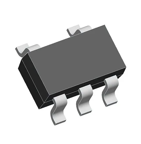
The LTP3456 family is offered in a small SOT23-5L and DFN1×1-4L packages, which are ideal for
small form factor portable equipment.
The LTP3456 family is available in standard fixed output voltages of 0.8 V, 1.2 V, 1.5 V, 1.8 V , 2.5 V, 2.8
V, 3.0 V, and 3.3 V.
Features and Benefits
◼ Wide Input Voltage Range from 1.9 V to 5.5 V
◼ Up to 500 mA Load Current
◼ Standard Fixed Output Voltage Options: 0.8 V, 1.2 V, 1.5 V, 1.8V, 2.5 V, 2.8 V, 3.0 V and 3.3 V
◼ Very Low IQ of 45 µA Typically
◼ Low Dropout of Typical 200 mV at 2.8 V Output and 300 mA Load
◼ High PSRR: 70 dB at 1 kHz
◼ Low Noise: 40 µVRMS at 1.2 V Output
◼ Excellent Load/Line Transient Response
◼ Packages:SOT23-5L, DFN1×1-4L
Applications
◼ Smart Phones and Tablets
◼ IP Cameras
◼ Portable instruments
CAUTION: These devices are sensitive to electrostatic discharge; follow proper IC Handling Procedures.
Linearin and designs are registered trademarks of LinearinTechnology Corporation.
©Copyright Linearin Technology Corporation. All RightsReserved.
All other trademarks mentioned are the property of their respective owners.
FN1621-42.0 — Data Sheet
High PSRR, 500 mA LDO
�LTP3456
P-2
Ordering Information
Model Note1
LTP3456
Package Name
Type Number Note1
Packing Quantity
SOT23-5L
LTP3456-xxNYT5
Tape and Reel, 3 000
DFN1×1-4L
LTP3456-xxNYF4
Tape and Reel, 10 000
Note1: xx stands for output voltage, e.g. if xx = 18, the output voltage is 1.8V; if xx = 30, the output voltage
is 3.0V. The device with suffix "N" is shutdown version with enable control input.
Pin Configurations (Top View)
IN
1
GND
2
EN
3
IN
EN
IN
EN
5
OUT
4
3
4
3
4
NC
1
2
1
2
OUT
GND
OUT
GND
SOT23-5
DFN1.0×1.0-4L
Pin Function
Package
SOT23-5L
DFN1×1-4L
Symbol
Function
1
4
IN
2
2
GND
Supply input pin.
Ground.
3
3
EN
Enable control input, active high.
4
/
NC
No Connection.
5
1
OUT
Output pin.
CAUTION: These devices are sensitive to electrostatic discharge; follow proper IC Handling Procedures.
Linearin and designs are registered trademarks of LinearinTechnology Corporation.
©Copyright Linearin Technology Corporation. All RightsReserved.
All other trademarks mentioned are the property of their respective owners.
FN1621-42.0 — Data Sheet
High PSRR, 500 mA LDO
�LTP3456
P-3
Block Diagram
IN
OUT
RLOW
Gate
Driver
EN
Current Limitand
Thermal
Shutdown
+
VREF
GND
Functional Description
INPUT CAPACITOR
A 1 μF ceramic capacitor is recommended to connect between VIN and GND pins to decouple input power
supply glitch and noise. The amount of the capacitance may be increased without limit. This input capacitor
must be located as close as possible to the device to assure input stability and less noise. For PCB layout, a
wide copper trace is required for both VIN and GND.
OUTPUT CAPACITOR
An output capacitor is required for the stability of the LDO. The recommended output capacitance is from 0.47
µF to 4.7 µF, Equivalent Series Resistance (ESR) is from 5 mΩ to 100 mΩ, and temperature characteristics is X7R
or X5R. Higher capacitance values help to improve load/line transient response. The output capacitance may be
increased to keep low undershoot/overshoot. Place output capacitor as close as possible to OUT and GND pins.
ON/OFF INPUT OPERATION
The LTP3456 is turned on by setting the EN pin high, and is turned off by pulling it low. If this feature is not used,
the EN pin should be tied to IN pin to keep the regulator output on at all time.
ULTRA FAST START-UP
After enabled, the LTP3456 is able to provide full power in as little as tens of microseconds, typically 80 µs. This
feature will help load circuitry move in and out of standby mode in real time, eventually extend battery life for
mobile phones and other portable devices.
CURRENT LIMIT PROTECTION
When output current at the OUT pin is higher than current limit threshold or the OUT pin is short-circuit to GND,
the current limit protection will be triggered and clamp the output current to approximately 500 mA to prevent
over-current and to protect the regulator from damage due to overheating.
THERMAL SHUTDOWN PROTECTION
Thermal protection disables the output when the junction temperature rises to approximately +155°C , allowing
the device to cool down. When the junction temperature reduces to approximately + 130°C the output circuitry is
enabled again. Depending on power dissipation, thermal resistance, and ambient temperature, the thermal
protection circuit may cycle on and off. This cycling limits the heat dissipation of the regulator, protecting it from
damage due to overheating.
CAUTION: These devices are sensitive to electrostatic discharge; follow proper IC Handling Procedures.
Linearin and designs are registered trademarks of LinearinTechnology Corporation.
©Copyright Linearin Technology Corporation. All RightsReserved.
All other trademarks mentioned are the property of their respective owners.
FN1621-42.0 — Data Sheet
High PSRR, 500 mA LDO
�LTP3456
P-4
Absolute Maximum Ratings
Parameter
Symbol
Min.
Max.
Unit
IN Voltage
VIN
–0.3
7
V
–0.3
VIN + 0.3
V
500
mA
DFN1×1-4L
180
°C/W
SOT23-5
260
°C/W
150
°C
150
°C
300
°C
Other Pin Voltage
Maximum Load Current
Package Thermal
Resistance
Junction Temperature
TJ
Storage Temperature
TSTG
Lead Temperature(Soldering, 10 sec)
–65
TL
NOTE:Stresses beyond those listed under “Absolute Maximum Ratings” may cause permanent damage to the
device. These are stress ratings only, and functional operation of the device at these or any other conditions
beyond those indicated in the operational sections of the specifications is not implied. Exposure to absolute
maximum rating conditions for extended periods may affect device reliability.
Recommended Operating Conditions
Parameter
Symbol
IN Voltage
VIN
Output Current
Min.
Max.
Unit
1.9
5.5
V
IOUT
0
500
mA
Operating Ambient Temperature
TA
-40
85
Effective Input Ceramic Capacitor Value
CIN
0.47
4.7
µF
Effective Output Ceramic Capacitor Value
COUT
0.47
4.7
µF
Input and Output Capacitor Equivalent
Series Resistance (ESR)
ESR
5
100
mΩ
Caution:
This integrated circuit can be damaged by ESD if you don’t pay attention to ESD protection. LINEARIN
recommends that all integrated circuits be handled with appropriate precautions. Failure to observe proper
handling and installation procedures can cause damage. ESD damage can range from subtle performance
degradation to complete device failure. Precision integrated circuits may be more susceptible to damage
because very small parametric changes could cause the device not to meet its published specifications.
LINEARIN reserves the right to make any change in circuit design, specification or other related things if
necessary without notice at any time. Please contact LINEARIN sales office to get the latest datasheet.
CAUTION: These devices are sensitive to electrostatic discharge; follow proper IC Handling Procedures.
Linearin and designs are registered trademarks of LinearinTechnology Corporation.
©Copyright Linearin Technology Corporation. All RightsReserved.
All other trademarks mentioned are the property of their respective owners.
FN1621-42.0 — Data Sheet
High PSRR, 500 mA LDO
�LTP3456
P-5
Electrical Characteristics
TA = +25°C, VIN = VEN = VOUT + 1 V unless otherwise noted.
Symbol Parameter
VIN
ΔVOUT
Test Conditions
Input Voltage Range
Regulated Output Voltage
IOUT = 1 mA,
-40℃≤ TA ≤85℃
Line Regulation
VIN = VOUT +1 V to 5.5 V, IOUT = 10 mA
Min
Max
Unit
1.9
Typ
5.5
V
–2
2
%VOUT
0.03
0.2
%VOUT
40
mA
Load Regulation
IOUT = 0 mA to 300 mA
20
TS
Soft-start Time
From enable to power on
80
µS
ISHORT
Short Current limit
VOUT = 0 V
70
mA
IQ-ON
DC Supply Quiescent Current
Active mode: VEN=VIN
45
70
μA
IQ-OFF
DC Supply Shutdown Current
VEN = 0V
0.01
1
μA
VDROP
Dropout Voltage
ILMT
Current Limit
PSRR
Power supply rejection ration
VOUT = 1.2 V, IOUT = 300 mA
380
480
mV
VOUT = 1.5 V, IOUT = 300 mA
300
400
mV
VOUT = 1.8 V, IOUT = 300 mA
220
340
mV
VOUT = 2.5 V, IOUT = 300 mA
210
330
mV
VOUT = 2.8 V, IOUT = 300 mA
200
320
mV
VOUT = 3.0 V, IOUT = 300 mA
190
310
mV
VOUT = 3.3 V, IOUT = 300 mA
180
300
mV
RLOAD = 1 Ω
300
mA
f = 1 kHz, COUT = 1 µF, IOUT = 20 mA
70
dB
f = 10 kHz, COUT = 1 µF, IOUT = 30 mA
65
dB
BW = 10 Hz to 100 kHz, IOUT = 200 mA,
VOUT = 2.8 V, COUT = 1 µF
60
μVRMS
BW = 10 Hz to 100 kHz, IOUT = 200 mA,
VOUT = 1.2 V, COUT = 1 µF
40
μVRMS
0.3
V
eN
Output Noise Voltage
VIL
EN Low Threshold
VIH
EN High Threshold
IEN
EN Pin Input current
RPD
EN pull-down resistance
RLOW
Output resistance of auto
discharge at off state
EN= 0 V,VIN= 4 V
90
Ω
TTSD
Thermal shutdown threshold
TJ rising
150
°C
THYS
Thermal shutdown hysteresis
TJ falling from shutdown
20
°C
1.2
VEN = 0 V
0.8
V
0
0.1
μA
1
1.3
MΩ
Note: Production test at + 25℃. Specifications over the temperature range are guaranteed by design
and characterization.
CAUTION: These devices are sensitive to electrostatic discharge; follow proper IC Handling Procedures.
Linearin and designs are registered trademarks of LinearinTechnology Corporation.
©Copyright Linearin Technology Corporation. All RightsReserved.
All other trademarks mentioned are the property of their respective owners.
FN1621-42.0 — Data Sheet
High PSRR, 500 mA LDO
�LTP3456
P-6
Application Circuits
VIN
VDD
VOUT
OUT
1µF
1µF
Enable
EN
GND
ON
OFF
CAUTION: These devices are sensitive to electrostatic discharge; follow proper IC Handling Procedures.
Linearin and designs are registered trademarks of LinearinTechnology Corporation.
©Copyright Linearin Technology Corporation. All RightsReserved.
All other trademarks mentioned are the property of their respective owners.
FN1621-42.0 — Data Sheet
High PSRR, 500 mA LDO
�LTP3456
P-7
Package Dimension
DFN1×1-4L
D
A2
A
E
e
A1
b
P1N1
Unit: mm
Symbol
Dimensions In Millimeters
MIN
MOD
MAX
A
0.450
0.500
0.550
A1
0.000
0.025
0.050
A2
0.125REF
D
0.950
1.000
1.050
D1
0.380
0.480
0.580
E
0.950
1.000
1.050
E1
0.380
0.480
0.580
b
0.150
0.200
0.250
e
0.650BSC
f
0.190
0.195
0.200
L
0.150
0.250
0.350
CAUTION: These devices are sensitive to electrostatic discharge; follow proper IC Handling Procedures.
Linearin and designs are registered trademarks of LinearinTechnology Corporation.
©Copyright Linearin Technology Corporation. All RightsReserved.
All other trademarks mentioned are the property of their respective owners.
FN1621-42.0 — Data Sheet
High PSRR, 500 mA LDO
�LTP3456
P-8
Package Dimension
SOT23-5L
θ
D
E
E1
L
b
c
e
Symbol
A
A2
A1
e1
Unit: mm
Dimensions In Millimeters
MIN
MAX
A
0.700
1.250
A1
0.000
0.100
A2
1.050
1.150
b
0.350
0.500
c
0.080
0.200
D
2.820
3.020
E
2.650
2.950
E1
1.600
1.700
e
0.950BSC
E1
1.800
2.000
L
0.300
0°
0.600
8°
Θ
CAUTION: These devices are sensitive to electrostatic discharge; follow proper IC Handling Procedures.
Linearin and designs are registered trademarks of LinearinTechnology Corporation.
©Copyright Linearin Technology Corporation. All RightsReserved.
All other trademarks mentioned are the property of their respective owners.
FN1621-42.0 — Data Sheet
High PSRR, 500 mA LDO
�


 工商网监
湘ICP备2023018690号
工商网监
湘ICP备2023018690号
