ESD Protection Diode
PDLLC03CI
Description
Features
PDLLC03CI a 3V bidirectional TVS diode, utilizing leading
monolithic silicon technology to provide fast response time
and low ESD clamping voltage, making this device an ideal
solution for protecting voltage sensitive high-speed data lines.
The PDLLC03CI has a low capacitance, and complies with
the IEC 61000-4-2 (ESD) standard with ±30kV air and ±30kV
contact discharge. It is assembled into a SOD-323 lead-free
package. The small size, low capacitance and high ESD
surge protection make PDLLC03CI an ideal choice to protect
cell phone, wireless systems,and communication equipment.
340W peak pulse power ( 8/20μs)
Ultra low capacitance :1.0pF typical
Ultra low leakage:nA level
Low Operating:3.3V
Low clamping voltage
Protects one power line or data line
Complies with following standards:
– IEC 61000-4-2 (ESD) immunity test Air
discharge: ±30kV
Contact discharge: ±30kV
– IEC61000-4-5 (Lightning) 21A (8/20μs)
RoHS Compliant
Mechanical Characteristics
Applications
Package: SOD-323
Lead Finish: Matte Tin
Case Material: “Green” Molding Compound.
Moisture Sensitivity: Level 3 per J-STD-020
Terminal Connections: See Diagram Below
Marking Information: See Below
Dimensions and Pin Configuration
Marking Information
USB Ports
Smart Phones
Wireless Systems
Ethernet 10/100/1000 Base T
CC
CC = Device Marking Code
Circuit and Pin Schematic
Ordering Information
Part Number
Marking
Packaging
Reel Size
PDLLC03CI
CC
3000/Tape & Reel
7 inch
www.pdwsemi.com
1 -4
© 2022 PDW, Inc.
Specifications are subject to change without notice.
Revised: 2022/04/08
�ESD Protection Diode
PDLLC03CI
Absolute Maximum Ratings (TA=25°C unless otherwise specified)
Parameter
Symbol
Value
Unit
Peak Pulse Power (8/20µs)
Ppk
340
W
Peak Pulse Current (8/20µs)
IPP
21
A
ESD per IEC 61000−4−2 (Air)
±30
VESD
ESD per IEC 61000−4−2 (Contact)
Operating Temperature Range
Storage Temperature Range
kV
±30
TJ
−55 to +125
°C
Tstg
−55 to +150
°C
Electrical Characteristics (TA=25°C unless otherwise specified)
Parameter
Reverse Working Voltage
Symbol
Min
Typ
VRWM
Max
Unit
3.3
V
Test Condition
Punch-Through Voltage
VPT
3.5
V
IT = 2µA
Snap-Back Voltage
VBR
4
V
IT = 1mA
Reverse Leakage Current
IR
100
nA
VRWM = 3.3V
Clamping Voltage
VC
6
V
IPP = 1A (8 x 20µs pulse)
Clamping Voltage
VC
16
V
IPP = 21A (8 x 20µs pulse)
Junction Capacitance
CJ
pF
VR = 0V, f = 1MHz
www.pdwsemi.com
1
2 -4
© 2022 PDW, Inc.
Specifications are subject to change without notice.
Revised: 2022/04/08
�ESD Protection Diode
PDLLC03CI
Typical Performance Characteristics (TA=25℃ unless otherwise Specified)
Junction Capacitance vs. Reverse Voltage
Peak Pulse Power vs. Pulse Time
Power Derating Curve
Clamping Voltage vs. Peak Pulse Current
100
% of Peak Pulse Current
90
80
70
60
50
40
30
20
10
Note:Data is taken with a 10x attenuator
0
0
20
40
Time_t(uS)
60
80
ESD Clamping Voltage
8 kV Contact per IEC61000−4−2
8 X 20μs Pulse Waveform
www.pdwsemi.com
3 -4
© 2022 PDW, Inc.
Specifications are subject to change without notice.
Revised: 2022/04/08
�ESD Protection Diode
PDLLC03CI
SOD-323 Package Outline Drawing
A
DIMENSIONS
MILLIMETERS
INCHES
MIN
MAX
MIN
MAX
1.50
1.80
0.060
0.071
SYM
B
1.20
1.40
0.045
0.054
C
2.30
2.70
0.090
0.107
D
-
1.10
-
0.043
E
0.30
0.40
0.012
0.016
F
0.10
0.25
0.004
0.010
H
-
0.10
-
0.004
Suggested Land Pattern
SYM
www.pdwsemi.com
4 -4
DIMENSIONS
MILLIMETERS
INCHES
A
3.15
0.120
B
0.80
0.031
C
0.80
0.031
© 2022 PDW, Inc.
Specifications are subject to change without notice.
Revised: 2022/04/08
�
很抱歉,暂时无法提供与“PDLLC03CI”相匹配的价格&库存,您可以联系我们找货
免费人工找货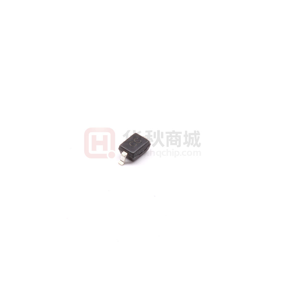


 工商网监
湘ICP备2023018690号
工商网监
湘ICP备2023018690号
