ETA1611
2A, 22V Step-Up Regulator
DESCRIPTION
FEATURES
The ETA1611 is a high efficiency step-up converter
with an internally integrated 22V power MOSEFT. It
runs with an optimal 1MHz frequency that enables
the use of small external components while still
providing the best efficiency. It can drive up to 2A
output current. The incorporated true PWM-Diming
feature through EN pin enable one further digitally
program the output voltage lower. For maximum
protection, the ETA1611 has an OVP protection
feature that prevents the output voltage exceeding
the maximum rating of the ETA1611 and the output
cap during open conditions.
Up to 95% Efficiency
22V OVP protection
True PWM Brightness Control
200mV Feedback Voltage
2.8A current limit
SOT23-6 Package
APPLICATIONS
ETA1611 is available in a space-saving SOT23-6
package.
Portable power bank
Powering 3G module
Large LCD display backlight driving up to 90 LEDs
Satellite STB
Bluetooth Speaker
Large TFT screen bias
Other application which needs high voltage and
high current generation
TYPICAL APPLICATION
VIN
2.7V to 6V
10μH
VOUT = 0.2V*(1+R1/R2)
10μF
1
5 IN
4.7μF
OFF
SW
ETA1611
ON
4
Or up to
90 LEDs
FB
R1
3
EN
R2
G
2
ORDERING INFORMATION
www.ETAsolution.com
PART No.
PACKAGE
TOP MARK
Pcs/Reel
ETA1611S2G
SOT23-6
GVYW
3000
Powering Minds of the Smarts
Proprietary Information DO NOT Distribute
1
�ETA1611
PIN CONFIGURATION
SW
1
GND
2
ETA1611
FB 3
ABSOLUTE MAXIMUM RATINGS
(Note: Exceeding these limits may damage the device. Exposure to
absolute maximum rating conditions for long periods may affect device
reliability.)
6
NC
5
IN
4
EN
SW Voltage............................................ –0.3V to 25V
All Other PIN Voltages………………..–0.3V to 6.5V
SW to ground current …………........Internally limited
Junction Temperature ...................................... 150°C
Storage Temperature Range …..….–55°C to 150°C
Thermal Resistance
θJA
θJC
SOT23-6…………………....134……50 ...........oC/W
SOT23-6
Recommended Operating Conditions
(Note: The device is not guaranteed to function outside its operating
conditions.)
Ambient Temperature Range .............–40°C to 85°C
Junction Temperature Range …......–40°C to 125°C
ELECTRICAL CHARACTERISTICS
(VIN = 3.6V, unless otherwise specified. Typical values are at TA = 25oC.)
PARAMETER
Input Voltage Range
Input UVLO
UVLO HYS
FB Feedback Voltage
FB Input Current
Quiescent Current at IN
Shutdown Supply Current at IN
Switching Frequency
Maximum Duty Cycle
NMOS Switch On Resistance
NMOS Switch Current Limit
SW Leakage Current
EN Input Low Voltage
EN Input High Voltage
Thermal Shutdown
CONDITIONS
Rising
MIN
2.7
2.00
VIN = VEN =3.6V
194
Switching at Iout=0
No Switching
VEN=GND
VIN2500
Sunlord
Schottky Diode Selection
A high-speed rectifying Schottky is recommended for ETA1611 for maximum efficiency due to its high switching
frequency. The diode average and peak current rating must be larger than the average output current and peak
inductor current to ensure reliability. In addition, the diode’s reverse breakdown voltage must exceed the open
LED protection voltage.
Input and Output Capacitor Selection
The output capacitor is mainly selected to meet the requirements for the output ripple and loop stability.
The output requires a capacitor in the range of 10μF to 22μF.
BLOCK DIAGRAM
EN
IN
UVLO &
Thermal
shutdown
REF
+
EA
+
-
Σ
-
FB
PWM
Logic
SW
DRIVER
OSC
Slope Comp
GND
Powering Minds of the Smarts
www.ETAsolution.com
Proprietary Information DO NOT Distribute
6
�ETA1611
PACKAGE OUTLINE
Powering Minds of the Smarts
www.ETAsolution.com
Proprietary Information DO NOT Distribute
7
�
很抱歉,暂时无法提供与“ETA1611S2G”相匹配的价格&库存,您可以联系我们找货
免费人工找货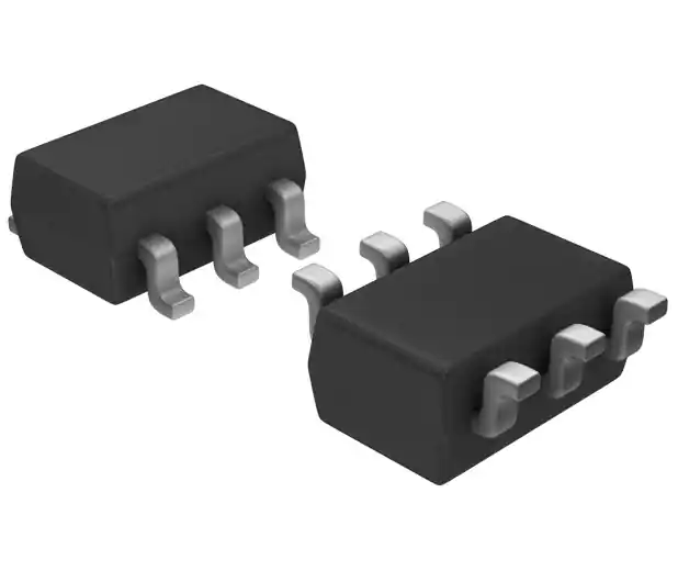


 工商网监
湘ICP备2023018690号
工商网监
湘ICP备2023018690号
