PIEZOELECTRIC ENERGY HARVESTERS
FEATURES
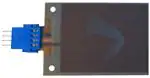
DESCRIPTION
�
Enables Vibration Energy Harvesting
�
Robust Piezo Packaging
�
Pre-Attached Electrical Lead Wires and Connector
�
Hermetically Sealed for Use in Harsh Environments
�
Low Profile
�
Available in Different Sizes to Match to Application
�
Directly Integrate with COTS Products Such As The
Linear LTC3588 and Thin Film Batteries
Volture™ vibration energy harvesters convert otherwise
wasted energy from mechanical vibrations into useable
electrical energy. The Volture™ accomplishes this by
utilizing normally brittle piezoelectric materials. The
Midé Volture™ energy harvester is unique amongst
other piezo based energy harvesters because it
incorporates Midé's patented piezoelectric transducer
packaging technology.
APPLICATIONS
�
Industrial Health Monitoring Network Sensors
�
Condition Based Maintenance Sensors
�
Wireless HVAC Sensors
�
Mobile Asset Tracking
�
Tire Pressure Sensors
�
Oil and Gas Sensors
�
All Air, Land and Sea Vehicle Sensors
�
Battery and Hard Wired Power Replacement
Through a proprietary manufacturing process, the
Volture™ packages piezoelectric materials in a
protective skin with pre-attached electrical leads,
producing a robust component with no soldered wires.
The Volture’s™ protective skin also provides electrical
insulation and defense against humidity and harsh
contaminants.
The Volture™ is available in six standard sizes. Custom
sizes are available and a cost effective alternative.
If a custom size is required please contact Midé
Technology Corporation by emailing:
volture@mide.com.
TYPICAL APPLICATION
CHARGE
MANAGEMENT
VIN
GND
VCC
OUT
VSTORE
MICRO
CONTROLLER
SENSOR
REVISION N0. 002
REVISION DATE: 01-23-2013
SENSOR
TX/RX
SENSOR
1
�PRODUCT DIMENSIONS
3.190
2.940
NOTE:
1. All dimensions are in inches
1.115
.865
.690
CLAMP LINE
2. Connector thickness = 0.100”
Product
Typical
Thickness (in)
V20W
0.034
V25W
0.024
V21B
0.031
V21BL
0.031
V22B
0.031
V22BL
0.031
.250
.600
1.31
1.250
1.500
.100
2X
1.81
V20W
V25W
.129
2.720
2.470
1.085
.910
CLAMP LINE
.570
.300
.175
V21B
.600 .660
1.400
2X
.100
.110
3.560
3.310
CLAMP LINE
1.085
.910
.300
.600 .660
.175
.570
2X
1.400
.110
V21BL
.100
2.533
2.283
CLAMP LINE
1.290
.883
V22B
.240 .600
.150
1.000
.100
3.633
3.383
1.290
CLAMP LINE
.883
.240 .600
.150
REVISION N0. 002
1.000
REVISION DATE: 01-23-2013
V22BL
.100
2
�ABSOLUTE MAXIMUM RATINGS
Operating Temperature Range
-40 to 90 C
Operating Temperature Range (Without Connector)
-40 to 150 C
Storage Temperature Range
-60 to 90 C
Storage Temperature Range (Without Connector)
-60 to 150 C
Lead Temperatures (Soldering, 10 sec)
300 C
Piezo Strain, max
800 micro-strain*
Maximum Voltage Output
Product and Vibration Dependent**
Maximum Current Output
Product and Vibration Dependent**
**See Performance Curves For Typical Values
*Related to max. tip deflection, see Deflection Limits
DEFLECTION LIMITS
Energy Harvester
Product Number
Max. Tip-to-Tip
Displacement (in)
V20W
0.10
V25W
0.15
V21B
0.06
V21BL
0.18
V22B
0.03
V22BL
0.12
TIP-TO-TIP
DISPLACEMENT
FIXED TO VIBRATING SURFACE
ELECTRICAL CHARACTERISTICS
V20W
Single Wafer Series
Capacitance (nF),
measured at 100 Hz
69
Single Wafer Series
Resistance (Ohm),
measured at 100 Hz
390
Single Wafer Series
Capacitance (nF),
measured at 120 Hz
69
Single Wafer Series
Resistance (Ohm),
measured at 120 Hz
340
V25W
130
210
130
175
V21B
26
950
26
770
V21BL
26
950
26
770
V22B
9
2400
9
2000
V22BL
9
2400
9
2000
Product
REVISION N0. 002
REVISION DATE: 01-23-2013
3
�PIN FUNCTIONS
P1, P2: Piezo wafer 1 output
P3, P4: Piezo wafer 2 output
Series
1234
1234
Parallel
OUT
OUT
OUT
OUT
Compared to Single Wafer Value
Same Voltage
Doubled Current
Capacitance: 2x the single-wafer value
Compared to Single Wafer Value
Double Voltage
Same Current
Capacitance: Half the Single-Wafer Value
Each Volture contains two electrically isolated piezo
wafers, which may be used independently or bridged
for increased voltage (series configuration) or current
output (parallel configuration). Series connection will
double the open-circuit voltage compared to a single
wafer, and the effective capacitance will be 1/2 the
single-wafer capacitance listed in the “Electrical
Characteristic Table (Pg. 3)”. Parallel connection will
double the current compared to a single wafer, and the
effective capacitance will be double the single-wafer
value. For most applications, parallel connection is
recommended. Please refer to the connection diagram
above. Regardless of series or parallel connection, the
power generated by the Volture™ Energy Harvester will
be the same.
In typical energy harvesting usage, the raw output is an
AC waveform as the Volture deflects in both directions.
For sensing or dual-use applications where it is desired
to know the direction of deflection at any given time,
please refer to the relationship between deflection and
output polarity for each wafer diagram below.
+
+
-
+
+
REVISION N0. 002
REVISION DATE: 01-23-2013
V20W
V25W
V21B / BL
V22B / BL
4
�OPERATION
The Volture™ vibration energy harvester is designed to
extract useable electrical energy from waste
mechanical vibrations. The best means to accomplish
this is to mount the Volture™ product in a cantilevered
configuration on the vibration source and tune the
natural frequency of the Volture™ harvester to match
that of the vibration source.
provided software allows the user to easily characterize
any vibration.
Attaching And Clamping The Volture™
For optimized energy harvesting from vibrations it is
best to mount the Volture™ products in a cantilevered
configuration. This takes advantage of resonant beam
harvesting. If the natural frequency of the Volture™ is
successfully tuned to that of the vibration source, the
most energy will be harvested.
Vibration Source Characterization
The first step in successful energy harvesting is to fully
understand the vibration environment in which the
Volture™ will be operating. The most effective means
to accomplish this is to measure the vibration using an
accelerometer, capture the data, and perform an FFT
(Fast Fourier Transform) on the data to extract the
relevant frequency information.
The first step in successful clamping is to ensure that
both the base and clamp are constructed of rigid
materials completely free of burrs and defects. Using a
rigid material will minimize dissipation of energy
through the clamp structure and avoiding burrs and
defects will minimize the potential for stress
concentrations on the Volture™ which could lead to
premature failure.
Some applications will not require this step since their
dominant frequencies are inherently known. An
example of this would be a 120 Hz AC motor or a 60
Hz appliance. However, most applications will require
some form of vibration characterization to be
successful.
The clamp should completely extend beyond the piezo
element within the Volture product. The suggested
clamp line shown in the product dimensions section of
this document ensures that the clamp is clamping on
the piezo element.
Midé offers a vibration characterization product and
service, the VR001. The VR001 is a small device that
can be easily installed into many different vibration
environments. The device is completely stand alone
and can be applied to hard to reach areas. Built in timer
delays allow for capture of many different types of
vibration environments. A simple USB interface with
For long term installation, the fasteners used to secure
the clamp should be properly torqued and should be
reinforced either using lock washers or some kind of
locking adhesive. This will ensure a proper long term
clamp that will not loosen over time.
TOP VIEW
TIP MASS
CLAMP LINE CLAMP CONNECTOR
SIDE VIEW
VIBRATION
BEAM SECTION FREE TO DISPLACE
REVISION N0. 002
FIXED TO VIBRATING SURFACE
REVISION DATE: 01-23-2013
5
�OPERATION
Straight clamps are the simplest and often most cost
effective clamps. However, curved clamps, as shown
in the diagram below, have shown the capability to
slightly increase performance of the Volture. Straight
clamps are sufficient for the majority of applications.
Tuning The Volture™
To ensure the most efficient harvesting, it is essential to
tune the Volture’s™ natural frequency to match that of
the vibrating source. Tuning is performed by adding a
tuning mass to the end of the cantilevered Volture™
CURVE CLAMP
until the natural frequency of the piezo beam is the
same as the vibration source. The larger the tuning
mass the lower the natural frequency of the Volture™.
For non permanent installations or for active tuning it is
best to use bee’s wax or some other form of nonpermanent attachment for the tuning mass to the
Volture. Bee’s wax allows the mass to be moved along
the beam, toward and away from the clamp, for tuning.
There are multiple means of tuning the Volture™
depending on the equipment available to the user. If
only the vibration source that will ultimately be
harvested from is available to the user, it is
recommended that the Volture™ be properly mounted
and clamped to the vibration source. The output of the
Volture should then be attached to an oscilloscope for
monitoring. The output can be either the raw output of
the Volture™ (directly on two of the output pins) or
through whatever electronics the user is using so long
as the electronics allow for some measure of optimal
REVISION N0. 002
power output. The tuning mass can then be adjusted
until the maximum power is achieved.
If the user has a shaker available, the tuning can be
performed by driving the Volture™ at the desired
natural frequency and adjusting the mass until optimal
power output is achieved. If connecting directly to the
Volture™ pins, optimal power output will be where the
voltage output is maximized.
Another simple way to tune your Volture™ product is to
measure the frequency at which the device "rings out"
when excited by an impulse mechanical load. The
easiest way to perform this type of tuning is to properly
mount and clamp the Volture to a rigid structure. Next,
attach at least one of the piezo's within the Volture
directly to an oscilloscope for monitoring (ex: connect
to pins P1 and P2). Add the appropriate tip mass (See
RELATION BETWEEN TIP MASS & NATURAL
FREQUENCY section) to the end of the cantilevered
Volture, do not permanently adhere the tip mass yet.
Bee's wax or tape is often the best material to use for
non permanent tip mass installations. Apply an impulse
mechanical load by very lightly "flicking" the end of the
Volture. This will cause the beam to "ring out". The
frequency of the the decaying wave is the natural
frequency that the Volture is currently tuned to. To
decrease this frequency move the mass farther away
from the clamp point, to increase the frequency move
the mass closer to the clamp point. If the natural
frequency is not close to the desired frequency either a
different tip mass or a different product may be
required.
Once the tip mass is in the proper location for optimal
energy harvesting it should be permanently adhered to
the Volture™. This ensures that the tip mass remains in
place for the life of the Volture™. It is recommended
that a robust adhesive such as Loctite™ 404 be used
for this permanent installation. Keep in mind that any
added mass will impact the tuning of the system.
REVISION DATE: 01-23-2013
6
�POWER MEASUREMENTS
Power Measurements
The power output capability of the Volture™ products
was measured in the following manner. In the
cantilevered beam configuration above, the Volture was
mounted to a shaker capable of generating vibrations of
varying frequency and amplitude. Tip masses (four for
each product) were added to alter the natural frequency
of the Volture™ products. The vibration frequency being
generated by the shaker was then matched to the
frequency of the Volture™ product to provide resonant
and therefore optimized energy harvesting. Four
different amplitudes were tested (0.25, 0.375, 0.5, and
1.00g) at each of these frequencies. The piezo’s output
was rectified and then placed across a purely capacitive
load. The capacitor value was chosen using the
following equation for average power, where C is the
REVISION N0. 002
capacitance in Farads, V is the piezo’s open circuit
voltage, and Δt is a reasonable time interval (~ 10
seconds), and solving for C:
PAVG
1 C V2
2
t
Yielding:
C
2 PAVG
V
t
2
The figure below shows the voltage (operating voltage)
on the capacitor and instantaneous power into capacitor
vs. time for a representative vibration level and
frequency. The V25W product was used, demonstrating
that the power increases until it peaks when the
operating voltage is at about half its open circuit value.
After that, it decreases.
See Application Note: Load Isolation Example.
Typical Power & Voltage vs Time
PPEAK
VOPEN CIRCUIT
Instantaneos Power (mW)
Piezoelectric material produces mechanical strain
under the influence of an externally applied electrical
field, and conversely produces electrical potential in
response to applied mechanical strain. Products such
as the Volture™ piezo energy harvester are typically
used in a cantilevered-beam configuration, in which the
piezoelectric beam is clamped at one end and the other
end allowed to oscillate freely in response to vibration
normal to the flat surface of the beam, converting
these vibrations to in-plane material strain. The beam
dimensions and tip mass determine the resonant
frequency of the beam, which is tuned to match the
dominant vibrational frequency of its environment,
mechanically amplifying this typically small vibration.
VOPEN CIRCUIT
0
Time (Seconds)
REVISION DATE: 01-23-2013
7
�V20W TYPICAL PERFORMANCE POWER CHARACTERISTICS
Tuned to 180 Hz | 0 gram Tip Mass
Tuned to 130 Hz | 2.4 gram Tip Mass
1.8
3
0.250 g, Pmax=0.159 mW
0.375 g, Pmax=0.328 mW
0.500 g, Pmax=0.606 mW
1.000 g, Pmax=1.719 mW
1.6
1.4
2
Power (mW)
1.2
Power (mW)
0.250 g, Pmax=0.272 mW
0.375 g, Pmax=0.573 mW
0.500 g, Pmax=0.883 mW
1.000 g, Pmax=2.692 mW
2.5
1
0.8
0.6
0.4
1.5
1
0.5
0.2
0
0
-0.2
-2
0
2
4
6
8
10
-0.5
-2
12
0
2
4
Operating Voltage
Tuned to 95 Hz | 7.8 gram Tip Mass
8
10
12
14
16
Tuned to 75 Hz | 15.6 gram Tip Mass
6
3.5
0.250 g, Pmax=0.532 mW
0.375 g, Pmax=0.969 mW
0.500 g, Pmax=1.428 mW
1.000 g, Pmax=3.005 mW
3
0.250 g, Pmax=0.717 mW
0.375 g, Pmax=1.470 mW
0.500 g, Pmax=2.394 mW
1.000 g, Pmax=5.860 mW
5
2.5
4
2
Power (mW)
Power (mW)
6
Operating Voltage
1.5
1
3
2
1
0.5
0
0
-0.5
-2
0
2
4
6
8
10
12
14
16
18
-1
-5
0
5
Operating Voltage
10
15
20
25
30
Operating Voltage
V20W RELATION BETWEEN TIP MASS & NATURAL FREQUENCY
160
Tip Mass
(gram)
150
Natural Frequency (Hertz)
140
130
120
110
100
90
80
70
60
0
2
4
6
8
10
12
14
16
Tip Mass (grams)
0
0
0
0
2.4
2.4
2.4
2.4
7.8
7.8
7.8
7.8
15.6
15.6
15.6
15.6
Fn
(Hz)
Amplitude
(g)
Open Circuit
Voltage*
180
180
180
180
130
130
130
130
95
95
95
95
75
75
75
75
0.25
0.375
0.5
1
0.25
0.375
0.5
1
0.25
0.375
0.5
1
0.25
0.375
0.5
1
4.7
6.5
7.7
12.8
6.7
9
11
18
8.3
11.8
16.4
23.1
13.3
19
22.6
34.7
* piezo wafers connected in series
REVISION N0. 002
REVISION DATE: 01-23-2013
8
�V25W TYPICAL PERFORMANCE POWER CHARACTERISTICS
Tuned to 120 Hz | 0 gram Tip Mass
Tuned to 75 Hz | 2.4 gram Tip Mass
2.5
1.6
0.250 g, Pmax=0.123 mW
0.375 g, Pmax=0.276 mW
0.500 g, Pmax=0.471 mW
1.000 g, Pmax=1.468 mW
1.4
1.2
2
1.5
Power (mW)
1
Power (mW)
0.250 g, Pmax=0.134 mW
0.375 g, Pmax=0.292 mW
0.500 g, Pmax=0.513 mW
1.000 g, Pmax=2.431 mW
0.8
0.6
1
0.5
0.4
0.2
0
0
-0.2
-2
0
2
4
6
8
10
-0.5
-2
12
0
2
4
Operating Voltage
Tuned to 50 Hz | 7.8 gram Tip Mass
8
10
12
14
16
18
Tuned to 40 Hz | 15.6 gram Tip Mass
10
8
0.250 g, Pmax=0.590 mW
0.375 g, Pmax=1.194 mW
0.500 g, Pmax=2.075 mW
1.000 g, Pmax=7.220 mW
7
6
0.250 g, Pmax=0.931 mW
0.375 g, Pmax=1.763 mW
0.500 g, Pmax=2.972 mW
1.000 g, Pmax=9.231 mW
8
6
Power (mW)
5
Power (mW)
6
Operating Voltage
4
3
4
2
2
1
0
0
-1
0
5
10
15
20
25
-2
-5
0
5
Operating Voltage
10
15
20
25
30
Operating Voltage
V25W RELATION BETWEEN TIP MASS & NATURAL FREQUENCY
130
Natural Frequency (Hertz)
120
110
100
90
80
70
60
50
0
1
2
3
4
5
6
7
8
Tip Mass (grams)
Tip Mass
(gram)
Fn
(Hz)
Amplitude
(g)
Open Circuit
Voltage*
0
0
0
0
2.4
2.4
2.4
2.4
7.8
7.8
7.8
7.8
15.6
15.6
15.6
15.6
120
120
120
120
75
75
75
75
50
50
50
50
40
40
40
40
0.25
0.375
0.5
1
0.25
0.375
0.5
1
0.25
0.375
0.5
1
0.25
0.375
0.5
1
3.2
4.4
5.5
10.1
4.7
6.5
7.5
11.5
10.3
15.4
18.6
29.5
14.5
21.2
27
36.6
* piezo wafers connected in series
REVISION N0. 002
REVISION DATE: 01-23-2013
9
�V21B TYPICAL PERFORMANCE POWER CHARACTERISTICS
Tuned to 275 Hz | 0 gram Tip Mass
Tuned to 175 Hz | 1 gram Tip Mass
0.3
0.7
0.250 g, Pmax=0.010 mW
0.375 g, Pmax=0.030 mW
0.500 g, Pmax=0.061 mW
1.000 g, Pmax=0.250 mW
0.25
0.5
Power (mW)
0.2
Power (mW)
0.250 g, Pmax=0.049 mW
0.375 g, Pmax=0.108 mW
0.500 g, Pmax=0.188 mW
1.000 g, Pmax=0.658 mW
0.6
0.15
0.1
0.05
0.4
0.3
0.2
0.1
0
0
-0.05
-1
0
1
2
3
4
5
6
-0.1
-2
7
0
2
4
Operating Voltage
6
8
10
12
Operating Voltage
Tuned to 140 Hz | 2.4 gram Tip Mass
Tuned to 105 Hz | 4.8 gram Tip Mass
2.5
1.4
0.250 g, Pmax=0.114 mW
0.375 g, Pmax=0.248 mW
0.500 g, Pmax=0.379 mW
1.000 g, Pmax=1.311 mW
1.2
0.250 g, Pmax=0.262 mW
0.375 g, Pmax=0.475 mW
0.500 g, Pmax=0.795 mW
1.000 g, Pmax=2.252 mW
2
1
Power (mW)
Power (mW)
1.5
0.8
0.6
0.4
1
0.5
0.2
0
0
-0.2
-2
0
2
4
6
8
10
12
14
16
18
-0.5
-5
0
5
Operating Voltage
10
15
20
25
Operating Voltage
V21B RELATION BETWEEN TIP MASS & NATURAL FREQUENCY
260
240
Natural Frequency (Hertz)
220
200
180
160
140
120
100
80
0
1
2
3
4
5
Tip Mass (grams)
Tip Mass
(gram)
Fn
(Hz)
Amplitude
(g)
Open Circuit
Voltage*
0
0
0
0
1
1
1
1
2.4
2.4
2.4
2.4
4.8
4.8
4.8
4.8
275
275
275
275
175
175
175
175
140
140
140
140
105
105
105
105
0.25
0.375
0.5
1
0.25
0.375
0.5
1
0.25
0.375
0.5
1
0.25
0.375
0.5
1
4.1
5.9
7.6
12.3
7.6
10.9
13.6
23.5
10.9
15.2
18.8
32
15.9
21.6
28.1
46.5
* piezo wafers connected in series
REVISION N0. 002
REVISION DATE: 01-23-2013
10
�V21BL TYPICAL PERFORMANCE POWER CHARACTERISTICS
Tuned to 110 Hz | 0 gram Tip Mass
Tuned to 65 Hz | 1 gram Tip Mass
0.3
0.6
0.250 g, Pmax=0.030 mW
0.375 g, Pmax=0.066 mW
0.500 g, Pmax=0.102 mW
1.000 g, Pmax=0.262 mW
0.25
0.2
0.4
Power (mW)
Power (mW)
0.250 g, Pmax=0.036 mW
0.375 g, Pmax=0.085 mW
0.500 g, Pmax=0.136 mW
1.000 g, Pmax=0.513 mW
0.5
0.15
0.1
0.3
0.2
0.05
0.1
0
0
-0.05
-1
0
1
2
3
4
5
6
7
8
-0.1
-2
9
0
2
4
Operating Voltage
6
8
10
12
14
Operating Voltage
Tuned to 50 Hz | 2.4 gram Tip Mass
Tuned to 40 Hz | 4.8 gram Tip Mass
3
1.6
0.250 g, Pmax=0.157 mW
0.375 g, Pmax=0.323 mW
0.500 g, Pmax=0.525 mW
1.000 g, Pmax=1.484 mW
1.4
1.2
0.250 g, Pmax=0.263 mW
0.375 g, Pmax=0.549 mW
0.500 g, Pmax=0.906 mW
1.000 g, Pmax=2.662 mW
2.5
2
Power (mW)
Power (mW)
1
0.8
0.6
1.5
1
0.4
0.5
0.2
0
0
-0.2
-5
0
5
10
15
20
25
-0.5
-5
0
5
Operating Voltage
10
15
20
25
30
Operating Voltage
V21BL RELATION BETWEEN TIP MASS & NATURAL FREQUENCY
130
120
Natural Frequency (Hertz)
110
100
90
80
70
60
50
40
0
1
2
3
4
5
Tip Mass (grams)
Tip Mass
(gram)
Fn
(Hz)
Amplitude
(g)
Open Circuit
Voltage*
0
0
0
0
1
1
1
1
2.4
2.4
2.4
2.4
4.8
4.8
4.8
4.8
110
110
110
110
65
65
65
65
50
50
50
50
40
40
40
40
0.25
0.375
0.5
1
0.25
0.375
0.5
1
0.25
0.375
0.5
1
0.25
0.375
0.5
1
3.95
5.35
6.6
12.1
8
9.9
12.4
22.1
9.8
13.7
19.1
27.5
13.2
19.2
25.9
44.4
* piezo wafers connected in series
REVISION N0. 002
REVISION DATE: 01-23-2013
11
�V22B TYPICAL PERFORMANCE POWER CHARACTERISTICS
Tuned to 240 Hz | 0 gram Tip Mass
Tuned to 125 Hz | 0.5 gram Tip Mass
0.06
0.14
0.25 g, Pmax= 0.00 mW
0.375 g, Pmax= 0.01 mW
0.5 g, Pmax= 0.01 mW
1.0 g, Pmax= 0.05 mW
0.05
0.1
Power (mW)
0.04
Power (mW)
0.25 g, Pmax= 0.01 mW
0.375 g, Pmax= 0.03 mW
0.5 g, Pmax= 0.06 mW
1.0 g, Pmax= 0.13 mW
0.12
0.03
0.02
0.01
0.08
0.06
0.04
0.02
0
0
-0.01
-0.5
0
0.5
1
1.5
2
2.5
3
3.5
4
-0.02
0
1
2
3
Operating Voltage
Tuned to 105 Hz | 1 gram Tip Mass
5
6
7
8
14
16
Tuned to 80 Hz | 2 gram Tip Mass
0.3
0.6
0.25 g, Pmax= 0.03 mW
0.375 g, Pmax= 0.06 mW
0.5 g, Pmax= 0.10 mW
1.0 g, Pmax= 0.26 mW
0.25
0.25 g, Pmax= 0.07 mW
0.375 g, Pmax= 0.17 mW
0.5 g, Pmax= 0.27 mW
1.0 g, Pmax= 0.59 mW
0.5
0.2
0.4
Power (mW)
Power (mW)
4
Operating Voltage
0.15
0.1
0.3
0.2
0.05
0.1
0
0
-0.05
-2
0
2
4
6
8
10
-0.1
-2
0
2
4
Operating Voltage
6
8
10
12
Operating Voltage
V22B RELATION BETWEEN TIP MASS & NATURAL FREQUENCY
260
240
Natural Frequency (Hertz)
220
200
180
160
140
120
100
80
0
0.5
1
1.5
2
Tip Mass (grams)
Tip Mass
(gram)
Fn
(Hz)
Amplitude
(g)
Open Circuit
Voltage*
0
0
0
0
0.5
0.5
0.5
0.5
1
1
1
1
2
2
2
2
240
240
240
240
125
125
125
125
105
105
105
105
80
80
80
80
0.25
0.375
0.5
1
0.25
0.375
0.5
1
0.25
0.375
0.5
1
0.25
0.375
0.5
1
2.2
3.4
4.6
7.2
6.7
9.3
11.6
18.5
9
12.1
14.7
25.1
13
17.4
22.3
33.4
* piezo wafers connected in series
REVISION N0. 002
REVISION DATE: 01-23-2013
12
�V22BL TYPICAL PERFORMANCE POWER CHARACTERISTICS
Tuned to 110 Hz | 0 gram Tip Mass
Tuned to 45 Hz | 0.5 gram Tip Mass
0.3
0.8
0.25 g, Pmax= 0.02 mW
0.375 g, Pmax= 0.04 mW
0.5 g, Pmax= 0.07 mW
1.0 g, Pmax= 0.21 mW
0.25
0.25 g, Pmax= 0.09 mW
0.375 g, Pmax= 0.17 mW
0.5 g, Pmax= 0.28 mW
1.0 g, Pmax= 0.75 mW
0.7
0.6
0.2
Power (mW)
Power (mW)
0.5
0.15
0.1
0.4
0.3
0.2
0.05
0.1
0
0
-0.05
-2
0
2
4
6
8
10
-0.1
-5
12
0
5
Operating Voltage
10
15
20
25
Operating Voltage
Tuned to 35 Hz | 1 gram Tip Mass
Tuned to 30 Hz | 2 gram Tip Mass
1.2
2
0.25 g, Pmax= 0.14 mW
0.375 g, Pmax= 0.30 mW
0.5 g, Pmax= 0.45 mW
1.0 g, Pmax= 1.05 mW
1
0.25 g, Pmax= 0.28 mW
0.375 g, Pmax= 0.48 mW
0.5 g, Pmax= 0.77 mW
1.0 g, Pmax= 1.84 mW
1.5
Power (mW)
Power (mW)
0.8
0.6
0.4
1
0.5
0.2
0
0
-0.2
-5
0
5
10
15
20
25
30
-0.5
-5
0
5
10
Operating Voltage
15
20
25
30
35
40
Operating Voltage
V22BL RELATION BETWEEN TIP MASS & NATURAL FREQUENCY
110
100
Natural Frequency (Hertz)
90
80
70
60
50
40
30
20
0
0.5
1
1.5
2
Tip Mass (grams)
Tip Mass
(gram)
Fn
(Hz)
Amplitude
(g)
Open Circuit
Voltage*
0
0
0
0
0.5
0.5
0.5
0.5
1
1
1
1
2
2
2
2
110
110
110
110
45
45
45
45
35
35
35
35
30
30
30
30
0.25
0.375
0.5
1
0.25
0.375
0.5
1
0.25
0.375
0.5
1
0.25
0.375
0.5
1
2
3.1
4.2
6.9
6
8.5
11
17.5
8
11.5
14
23.4
12
16.1
20.8
31.8
* piezo wafers connected in series
REVISION N0. 002
REVISION DATE: 01-23-2013
13
�APPLICATIONS INFORMATION - SWITCHED CAPACITOR BOOST CIRCUIT
Switched Capacitor Boost Circuit for OneShot Sensors and Low Vibration Levels
It is often difficult to make use of low-voltage energy
scavenging sources, such as piezo energy harvesters
at low vibration amplitudes, solar cells in overcast or
indoor environments, or Seebeck devices, etc., as
most microcontrollers and sensors require minimum
voltages of 1.8V or greater to operate. Using these
sources requires a voltage boost converter with a
minimum start-up voltage, low start-up current
requirement, and graceful handling of undervoltage and
slow input voltage rise times.
The circuit shown, based on the Seiko Epson S-882Z
series charge pump IC, provides bursts of power
starting at approximately 2.4VDC (ending at 1.6-2
VDC) from input voltages as low as approximately
380mV. This IC provides boosting using small on-chip
switched (“flying”) capacitors, rather than inductive
boost conversion. Thus the initial input current
requirements are reduced compared to a typical boost
conver ter, requiring only a small power-supply
bypass capacitance to reliably start up. The circuit
can begin operating almost immediately when power
becomes available. This circuit is ideal for directly
powering small sensors that can perform their
function (e.g. record or transmit a measurement) in a
known amount of time and power. It could also be
used to extend battery life, or as a trigger source for
devices with their own battery/supercap power
source.
When the voltage at VIN exceeds the minimum start-up
voltage, the IC begins pumping charge to a storage
capacitor connected across the CPOUT pin. When the
capacitor voltage reaches 2.4V, the output is enabled
and this voltage is applied to the load. The load is
automatically disconnected when the storage capacitor
voltage drops below approx. 1.8V (see Figure 6). This
behavior allows the circuit to directly power most 3.3V
microcontroller circuits, with a typical operating voltage
range of 1.8V ~ 3.6V, without exposing the circuit to
significant undervoltage or unfavorable voltage risetime conditions.
S-882Z
VH
4
5
Piezo Bimorph
D1
VM
VIN
GND
CPOUT
VOUT
J3
X1
2
1
VCC
BAT54STA
U1
C1
X2
3
10uF
1
QPXX_RA
D2
GND
C3
100uF
GND
GND
REVISION N0. 002
REVISION DATE: 01-23-2013
14
�APPLICATIONS INFORMATION - SWITCHED CAPACITOR BOOST CIRCUIT
Goals
� Allow intermittently operating circuits to be
powered from extremely weak vibration sources,
or moderate vibration sources at frequencies significantly different from the energy harvester's resonant frequency (Figure 3)
�
�
Physically disconnect the load during periods of
insufficient voltage to avoid "over-the-hump" problems of cold circuit start-up from harvested power
Maximize chances of success where vibration
source's characteristics (amplitude and frequency
content) cannot be known in advance.
Simple “One-Shot” Application
A simple usage scenario is an embedded sensor with
data storage/transmission capability, which takes one
set of measurements each time it is powered up
(relying on the loss and subsequent re-application of
power to start the next measurement). In this case, the
measurement frequency is variable and depends on the
vibration amplitude. To operate the sensor directly from
the boost circuit requires:
�
Estimation (or measurement of) the run-time and
power consumption of your application within its
voltage limits
�
Sizing the CPout according to worst-case usage,
allowing some headroom
For such one-shot sensors, it is recommended to
create a large load (e.g. drive an LED or GPIO pin tied
to ground) after completing the task in order to ensure
the power output cycles in high-vibration conditions.
A typical microcontroller sensor application’s load
profile will be “bursty”, complicating the task of
estimating the required value of CPout. However, if the
load can be approximated in terms of a resistive load,
the following equations can be used to estimate the
required capacitance, available runtime, energy per
discharge or power stored.
REVISION N0. 002
1
C
V
1
R ln o
Td
V
Equation 1: Capacitance needed for
a given runtime (F)
Td
R C ln
Vo
V
Equation 2: Runtime for a given
capacitance (sec.)
W
1
2
C V0
2
V
2
Equation 3: Energy per discharge
(Joules or watt-seconds)
P
W
Tc
Td
Equation 4: Average Power (Watts)
In the equations above, Td is the runtime or discharge
time in seconds, Tc is the charge time in seconds, R is
the equivalent load resistance in ohms, V0 is the
starting output voltage (2.4), V is the final output
voltage (1.8V or the minimum operating voltage of the
sensor, whichever is greater), and C is the capacitance
in Farads. Likewise, the output voltage can be modeled
as a simple RC time constant, V = V0e-T/RC.
Continuously-Powered Application with
Input-Dependent Triggering
Sometimes it may be advantageous to incorporate
vibration-powered battery maintenance and/or
triggering into a continuously-running circuit. For
example, a sensor may require low-level continuous
power to maintain a realtime clock, but measurement
tasks are only needed when a piece of machinery is
known to be operating. Alternately, it may be desired to
dynamically adjust the measurement rate based on the
incoming power to maintain a given power budget. In
REVISION DATE: 01-23-2013
15
�APPLICATIONS INFORMATION - SWITCHED CAPACITOR BOOST CIRCUIT
these cases, the application can use Vout as an
interrupt source in addition to power source, with a
rising or falling edge triggering the desired action.
Typical Results
The following are measured results using the circuit
shown in a typical configuration.
Discharge Interval vs. Acceleration
Averaged Power Output vs. Acceleration
Volture V20W @ 60Hz, 100uF
10
Volture V20W @ 60Hz
3
90
10
10
Average power output (uW)
Time between discharge cycles (s)
80
2
1
70
60
50
40
30
20
10
10
0
0
0.1
0.2
0.3
0.4
0.5
0.6
0.7
0
0
0.1
Acceleration (g)
0.2
0.3
0.4
0.5
0.6
0.7
Acceleration (g)
Figure 2: Discharge Interval vs. Acceleration, measured
results using configuration shown
Figure 4: Averaged Power Output vs. Acceleration
Usable Bandwidth vs. Acceleration
Volture V20W
Usable V20W bandwidth at Fc=60Hz (Hz)
60
50
40
30
20
10
0
0.2
0.3
0.4
0.5
0.6
0.7
0.8
0.9
1
1.1
1.2
Acceleration (g)
Figure 3: Usable Bandwidth vs. Acceleration at 60Hz center
frequency. Usable bandwidth refers to the frequency range
over which the setup produced voltages exceeding the
circuit’s turn-on threshold (2.4V), producing output pulses.
REVISION N0. 002
REVISION DATE: 01-23-2013
16
�APPLICATIONS INFORMATION - SWITCHED CAPACITOR BOOST CIRCUIT
Tek Stop
Tek Stop
: 570mV
@: 2.42 V
: 570mV
@: 2.42 V
3
3
Ch1 500mV
Ch2 500mV
Ch3 500mV
M 2.00 s
A Ch1
0.00 V
Figure 5: Rectified input (aqua), VCAP (navy) and switched
output (violet) from initial start-up to stable output, 10K
resistive load.
REVISION N0. 002
Ch1 500mV
Ch2 500mV
Ch3 500mV
M 200ms
A Ch1
0.00 V
Figure 6: Rectified input (aqua), VCAP (navy) and switched
output (violet) output pulse detail, 10K resistive load.
REVISION DATE: 01-23-2013
17
�APPLICATIONS INFORMATION - LOAD ISOLATION EXAMPLE
Load Isolation Example for Maximum
Efficiency with Low-Impedance Loads
A cantilevered-beam piezoelectric energy harvester is a
complex electromechanical system in which the
electrical and mechanical loading of the beam are interrelated. Understanding of this relationship is critical to
getting the most out of the system.
R
R
A properly tuned switched boost-buck circuit will
always outperform any circuit in which you do not
tune to the characteristics of its application. This
application note demonstrates a high-efficiency
switched step-down (buck) converter and
optimizations for maximum performance in a realworld application. This circuit isolates the endapplication’s electrical load from the piezo beam,
providing proper impedance-matching of the circuit’s
“virtual load” to the beam, as well as minimizing
mechanical loading effects. Such a circuit is ideal for
low-impedance loads such as rechargeable batteries,
“bursty” loads such as intermittently-operating
sensors/transmitters, and applications where the
electrical load cannot be known in advance.
Basic Piezoelectric Beam Model
Before mechanical loading effects are taken into
account, each piezo beam can be thought of as a small
current source in parallel with a capacitor and parasitic
resistance, as shown in Figure 1. Typical values for this
parallel capacitance and resistance are on the order of
10nF and >40M, respectively. This parallel resistance
is insignificant for our purposes and may be ignored.
The current flow is equal to the derivative of the straininduced charge, or dQ/dt. The voltage transfer function
of each beam therefore is V(s)/q(s) = sR/(1+sRC),
where R is the parallel resistance and C is the parallel
capacitance of the beam.
In its simplest form, power is drawn from a small
capacitor which is constantly recharged by its
REVISION N0. 002
leak
leak
Figure 1: Piezo parallel and series equivalent circuits
environment. Care must be taken to choose when this
power is drawn. To maximize transfer efficiency, the
load must be matched to the piezo’s equivalent
impedance. In practice, the piezo impedance at a given
amplitude and frequency, as well as the load
impedance, can be thought of as a pair of simple (but
unknown) resistances which make up a resistor
divider. The power transfer between the two is
optimized when their values match. This corresponds
to the point at which the piezo’s loaded voltage is equal
to half its open-circuit voltage. Thus the impedance
match can be optimized without formally measuring or
knowing the impedance of the piezo source or load insitu.
Implementation
The circuit of Figure 2 provides a simple but effective
approach to meeting these goals.
The main components are a bridge rectifier formed by
D1-D4, low-power comparator (U1) and buck
converter (U2). During vibration, main storage
capacitor C1 slowly charges until its voltage reaches
the operating point (Voc/2) set by R1 and R2. Buck
converter U2 is enabled once the stored voltage
exceeds this value plus a small hysteresis. At typical
loads, the buck converter operation into the load will
REVISION DATE: 01-23-2013
18
�APPLICATIONS INFORMATION - LOAD ISOLATION EXAMPLE
VCC
R3
R5
2.2M
D8
+ C3
R7
VOUT
4.7M
1
2
5 SW
4
V4
BAT43W
VOUT
12pF
GND
1uF
R8
C2
VFB
U2 D6
7
VIN
VFB
6
SENSE LBO
3
1
LBI
SW
RUN 8
RUN
GND
LTC1474CMS8
VCC
R6
2.4M
LTC154 0CMS8
100K
BAT43W
100uH
8
OUT
7
V+
2
V-
BAT43W
R4
D2
1
-IN
3
+IN
5
HYS
6 REF
D7
R1
5.7M
C
100uF
1M
X2
BAV199
BAV199
R2
X1
+ C1
V REF
GND
D1
A
Piezo Bimorph
Zener 11V
D5
15M (Optional)
10nF
GND
Figure 2: Simple high-efficiency voltage conversion and load-isolation circuit for piezo energy harvesting applications. The C1
voltage setpoint in this example is fixed, but could be made adaptive using additional circuitry.
deplete C1 until its voltage drops below the hysteresis
band, at which point the converter is disabled and the
cycle repeats. Thus C1 is maintained at approximately
Voc/2. The typical output is a train of voltage-regulated
pulses ideally suited to charging a battery or capacitor,
or directly powering an intermittently-operating sensor.
Since the voltage at C1 is held approximately constant,
the effective load seen by the piezo is not significantly
affected by activation of U2 or changes to the actual
load. Additionally, the voltage maintained on C1
ensures charge is drawn from the piezo beam only
when its voltage exceeds C1’s voltage by one diode
drop, which occurs only when the beam approaches its
maximum deflection. Thus a limited amount of charge
is drawn on each cycle of the piezo beam, timed to
coincide with the maximum deflection of the beam.
This combination of factors helps prevent excessive
mechanical damping of the beam, allowing usable
output voltages to be output at lower vibration
amplitudes while the piezo beam is driven near its
mechanical resonance.
U2 provides a regulated output voltage determined by
the ratio of R7 and R8. The power output per G of
vibration will remain relatively constant across G-levels
and loads, provided the load is capable of drawing at
REVISION N0. 002
least as much power as is being supplied (Figure 5).
The converter duty cycle is approximated by the ratio
of input power (G-level) vs. output power (voltage *
current * time), less any small conversion losses and
leakage. When the input power exceeds the output and
losses, duty cycle will be 100%, and excess voltage at
C1 is safely disposed of through D5.
R6 sets the peak current through inductor L1, and can
be specified according to the equation:
R SENSE
0.067
I MAX
0.25
where IMAX is the maximum desired output current to
the load. Generally, the peak inductor current should be
set to maximum to improve efficiency with smaller
( 1mA,
the DC bias current (from 9uA at no load to 100uA in
continuous mode) is negligible compared to the gate
charge losses. Each time the gate is switched on and
off, a packet of charge dQ moves from VIN to ground.
In continuous mode, IGATE = fQp where Qp is the gate
charge of the internal switch and f is the switching
frequency. Since VIN is pre-set according to piezo
efficiency considerations, the best way to minimize this
loss is to keep the output duty cycle low.
Resistive (I2R) Losses
The resistances in the current path (The ON-resistance
REVISION N0. 002
of the internal switch, current sense resistor, and
inductor) contribute resistive losses. At low values of
VIN, switch losses will dominate, and can be minimized
by using a suitably large inductor and low IPEAK. At
higher supply voltages, these losses are proportional to
load.
Catch Diode Losses
The catch diode, D7, introduces a loss (V*I) as it
conducts during the switch off-time, proportional to its
forward voltage, and more pronounced at high supply
voltage where the switch on-time is shorter. Again, VIN
is fixed for piezo efficiency reasons, so this loss is best
minimized by minimizing the diode Vf and converter
duty cycle. By lowering the duty cycle, a reduction in Vf
of the catch diode will improve efficiency even though
low-Vf diodes tend to have much higher reverse
leakage currents, which will produce loss during the
switch ON-time. In any event, the catch diode must be
sized to safely handle IPEAK at nearly 100% duty cycle
(worst-case condition; output shorted).
The selection of 100uH inductor should be considered
a minimum, for use in conjunction with high IPEAK
values. Particularly in applications where space is not
constrained or IPEAK must be reduced, inductors as
large as 1000uH may be required for maximum
efficiency. The ideal range of inductor size at a given
IMAX is a trade-off between the increased resistance of
higher-value inductors and the increased switching
rates required for lower-value inductors.
At light loads, the output duty cycle will rise and losses
in the conversion stage (leakage, switching and catch
diode losses) will accrue. This may or may not be a
problem; it could simply mean that more power is
available than the load can use.
REVISION DATE: 01-23-2013
20
�APPLICATIONS INFORMATION - LOAD ISOLATION EXAMPLE
Application Example
The steps to configure this circuit optimally for a given
load are presented below. This example assumes the
following are known:
�
Required output voltage
�
Required output current
�
Nominal piezo open-circuit voltage
The LTC1540 features a programmable hysteresis
band of up to 100mV. However, a larger hysteresis is
generally preferable to allow for smaller values of C1
and/or longer output ON-times, particularly for directlypowered sensors. This can be accomplished by
bypassing the onboard hysteresis adjustment (R4=0
ohms; R5=open) and adding a small amount of
positive feedback via R3.
1) Set output voltage
The output voltage is determined by
Vout = 1.23 1+
R7
R8
(Circuit adaptations for self-adjusting bias voltage may
be explored if the power gains exceed the consumption
of the added circuitry.)
V
Where Vf is the forward voltage drop of D8 under load.
In direct sensor-power applications where reverse
leakage into the circuit during its off-time is not a
concern, D8 may be omitted (but see important
warnings below). To minimize no-load supply current,
resistor values in the megaohm range should be used.
2) Choose inductor size and maximum inductor
current, following the guidelines of the LT1474
datasheet. For greatest efficiency where space is not a
concern, first choose the inductor current sense
resistor R6 according to desired output current
(RSENSE Equation above), then size the inductor
accordingly. For space-limited applications, size L1 as
dictated by the available space and set IPEAK as high
as the inductor will tolerate without saturating.
3) Choose C1 bias voltage to be approximately ½ the
open-circuit piezo voltage in its natural vibration
environment. In applications with highly variable
amplitudes, a trade-off must be made between
efficiency at higher amplitudes and the ability to
harvest power from lower amplitudes: no charge will
be drawn by this circuit if the piezo open-circuit voltage
after rectification never reaches the set turn-on voltage.
REVISION N0. 002
First select the desired center voltage (Vc) for C1 and
the desired hysteresis band (Vhb). Choose a value for
R1 such that the current across it at the trip point is
substantially greater than the comparator’s input
leakage (1nA typ.), for example 100nA. The 5.7M value
shown is perfectly reasonable, but the following will
more formally dictate its upper limit. The LTC1540’s
internal reference (Vref) is 1.182V. The current through
R1 at the lower trip point is (Vc-(Vhb/2)-Vref) / R1.
Thus the upper limit for R1 is
Vhb
2
I R1
Vc
R1
1.182
Choose R2 to set the center voltage, Vc. Neglecting the
small influence of R3,
R2
1.182 R1
Vc 1.182
Choose R3 to set the hysteresis. At the lower
comparator trip point, the threshold voltage will be
equal to
VL
REVISION DATE: 01-23-2013
R2
R2
R1 R3
21
�APPLICATIONS INFORMATION - LOAD ISOLATION EXAMPLE
as the comparator will be ON when approaching this
point. Solving for R3,
R3
R1 R2 VL Vth
R1 Vth R2 Vth R2 VL
The addition of R3 will slightly affect the actual center
voltage; however, this change will typically not be
significant in comparison with the size of the hysteresis
band. For a typical Vc (>3.3V), the final value of Vc will
be lowered. As indicated by Figure 5, however, driving
the piezo to moderately higher open-circuit voltages
than optimal does not have an excessive impact on
efficiency.
Check: Actual Vh and Vl
Once all resistor values are chosen, the actual upper
and lower trip points will be defined by:
Vh 1.182
R2 R3 R1
R2 R3
Vl 1.182
R1 R3 R2
R2
REVISION N0. 002
Latch-Up Consideration
If diode D8 is removed, the designer must pay attention
to D6, which is necessary to prevent latch-up of the
LT1474’s output switch if the voltage at its SW pin is
held up while VIN drops. This situation may easily
occur in an application where the load is powered by
multiple sources or includes a storage element, such
as supercapacitor or battery, whose voltage drops
more slowly than that of C1 when no harvested power
is available. The user must then choose D6 so that the
voltage at SW cannot exceed the voltage at VIN by the
0.6V required for latch-up. Particularly at high C1
voltages, the designer must also take steps to ensure
that reverse leakage over D6 will not allow the voltages
at the VFB and SW pins to float above their maximum
ratings at no load.
REVISION DATE: 01-23-2013
22
�APPLICATIONS INFORMATION - POWER MANAGEMENT IC INTEGRATION
Integration with LTC3588 Charge
Management IC
The LTC3588-1 is an ultra low quiescent current power
supply designed specifically for energy harvesting
applications. The part is designed to interface directly to
a piezoelectric or alternative A/C power source such as
the Volture™. The part rectifies a voltage waveform and
stores harvested energy on an external capacitor,
bleeds off any excess power via an internal shunt
regulator, and maintains a regulated output voltage by
means of a nanopower high efficiency synchronous
buck regulator. When combined with a Volture™ energy
harvester the LTC3588-1 forms the base of a full energy
harvesting solution.
advantage of the high voltage input since the buck
converter on the chip can deliver 100mA average
current efficiently to the load. The input capacitor
should then be sized to store enough energy to provide
output power for the length of time required, while also
not dropping to the undervoltage lockout falling
threshold (UVLO falling). This threshold is
approximately 300mV above the selected regulated
output. The following simple equation shows energy
out on the left-hand side, and effective energy in on the
right-hand side.
The LTC3588-1 will gather energy and convert it to a
useable output voltage to power any type of electronic
system. Some applications may require much more
peak power than a typical piezo can produce. The
LTC3588-1 accumulates energy over a long period of
time to enable efficient use for short power bursts. The
frequency of bursts allowed is directly proportional to
the power coming in from the piezo, and the total energy
per burst. The LTC3588-1 allows for four different pin
selectable output voltages (1.8, 2.5, 3.3 and 3.6).
and
PGOOD Signal
The PGOOD Signal is a logical high when VOUT reaches
92% of the target value. This behavior is ideal for an
enable or interrupt pin on a microprocessor. That way,
the microprocessor can be idle until there is enough
energy to supply the burst.
Capacitor Selection
The input and output capacitors should be selected
based on the energy needs and load requirements of
the application. The VIN capacitor is placed between
VIN and GND. It should be rated to withstand the
highest voltage that the piezo can put out. For 100mA
or smaller loads, storing energy at the input takes
REVISION N0. 002
2
1
P LOAD t LOAD 2 C IN V IN
V UVLOFALLING
2
V UVLOFALLING VIN V SHUNT
Where η is the efficiency of the buck converter, and
VSHUNT is the voltage at which the input shunt
regulator bleeds power from the input (typically 20V).
See LTC3588 datasheet for more detail on η, as it
depends on the selected regulated output, the value of
the inductor, the load current, and temperature.
Keeping CIN at this value or greater ensures that there
is enough power stored at the input to perform each
burst.
To size the output capacitor, the following equation is
used:
t SLEEP C OUT
24mV
I LOAD
For capacitor values on the order of 10uF, some nonideal delays are introduced, resulting in VOUT ripple.
For smoother operation, it is recommended that COUT
be kept higher than 10uF.
REVISION DATE: 01-23-2013
23
�APPLICATIONS INFORMATION - POWER MANAGEMENT IC INTEGRATION
VIN2 and CAP Capacitors
A 1uF capacitor should be connected between VIN and
CAP and a 4.7uF capacitor should be connected
between VIN2 and GND. These capacitors hold up the
internal rails during buck switching and compensate
the internal rail generation circuits. In applications
where the input source is limited, to less than 6V, the
CAP pin can be tied to GND and the VIN2 pin can be tied
to VIN. In this scenario, a 5.6V Zener diode can be
used to clamp VIN.
Inductor
The buck converter is optimized to work with an
inductor in the range of 10uH to 100uH. 10uH is
adequate for space-limited applications, but 100uH
may provide greater efficiency, particularly as the ratio
between input and output voltage increases (see
LTC3588 datasheet). Choose an inductor with a DC
current rating greater than 350mA. Lower DCR
inductors can impact the efficiency of the buck
converter.
PZ2
PZ1
10uF
25V
1uF
6V
4.7uF
6V
LTC3588-1
100uH
CAP
SW
VIN2
VOUT
D1
D0
EN
PGOOD
VIN
3.3V
TX
MICROPROCESSOR
CORE
GND
47uF
6V
GND
REVISION N0. 002
REVISION DATE: 01-23-2013
24
�


 工商网监
湘ICP备2023018690号
工商网监
湘ICP备2023018690号
