Electronics, Inc.
2590 North First Street, San Jose, CA 95131, U.S.A.
Tel: 408-732-5000
Fax: 408-732-5055
http://www.atpinc.com
Rev. Date: Dec. 01. 2014
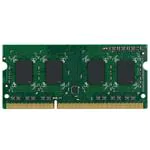
ATP AW12M7218BLK0MW
4GB DDR3-1600 Wide Temperature
UNBUFFERED ECC SODIMM
DESCRIPTION
The ATP AW12M7218BLK0MW is a high performance 4GB DDR3-1600 Industrial Grade Unbuffered ECC
SODIMM SDRAM memory module. It is organized as 512M x 72 in a 204-pin Small Outline Dual-In-Line
Memory Module (SODIMM) package. The module utilizes nine 512Mx8 DDR3 SDRAMs in FBGA package.
The module consists of a 256-byte serial EEPROM, which contains the module configuration information.
KEY FEATURES
Operation Temperature(TA): -40°C ~ +85°C
High Density:
4GB (512M x 72)
DIMM Rank:
1 Rank
Cycle Time:
1.25ns (800MHz)
CAS Latency: 11
Power supply: 1.5V ± 0.075V
Internal self calibration through ZQ
Burst lengths:
8
Part No.
AW12M7218BLK0MW
Auto & Self refresh
Asynchronous Reset
7.8 s refresh interval at lower than TCASE
85°C, 3.9s refresh interval at 85°C < TCASE
< 95 °C
Dynamic On Die Termination
Fly-by topology
PCB Height: 1.18 inches
RoHS compliant
Max Freq
800MHz (1.25ns@CL=11) x2
Interface
SSTL_15
PIN DESCRIPTION
Pin Name
Description
Pin Name
Description
A0~A9, A11~A15
A10/AP
BA0~BA2
CAS
CK0~CK1
CK0 ~ CK1
CKE0
DM0~DM8
DQ0~DQ63
DQS0~DQS8
Address Inputs
Address Input/Auto precharge
SDRAM Bank Address
Column Address Strobe
Clock Inputs, positive line
Clock Inputs, negative line
Clock Enables
Data Masks
Data Input/Output
Data strobes
ODT0
RAS
CS0
SA0~SA1
SCL
SDA
VDD
VDDSPD
VSS
RESET
On die termination
Row Address Strobe
Chip Selects
SPD address
Serial Presence Detect (SPD) Clock Input
SPD Data Input/Output
Core Power
SPD Power
Ground
This signal resets the DDR3 SDRAM
DQS0 ~ DQS8
VREFDQ VREFCA
A12/ BC
VTT
CB0~CB7
Data strobes, negative line
Input/Output Reference
Address Input/Burst chop
Termination voltage
DIMM ECC Check bits
WE
Event
NC
Write Enable
Temperature sensor Event output
No Connect
Logic Analyzer specific test pin (No connect
on SO-DIMM)
TEST
Your Ultimate Memory Solution!
Page 1 of 7
�ATP AW12M7218BLK0MW
PIN ASSIGNMENT
No.
Designation
No.
Designation
No.
Designation
No.
Designation
1
3
5
7
9
VREFDQ
VSS
DQ0
DQ1
VSS
2
4
6
8
10
VSS
DQ4
DQ5
VSS
A1
A0
VDD
CK0
106
108
110
112
114
A2
BA1
VDD
CK1
DQS0
105
107
109
111
113
11
13
15
17
DM0
DQ2
DQ3
VSS
12
14
16
18
DQS0
VSS
DQ6
DQ7
115
117
119
121
VDD
A10/AP
BA0
19
21
DQ8
DQ9
20
22
VSS
DQ12
123
125
23
VSS
24
DQ13
127
25
26
VSS
27
29
DQS1
DQS1
VSS
28
30
DM1
31
33
35
DQ10
DQ11
VSS
37
39
41
43
45
47
49
DQ16
DQ17
VSS
DQS2
DQS2
VSS
DQ18
51
53
55
57
59
CK0
WE
VDD
116
118
120
122
CK1
VDD
NC
NC
RAS
VDD
ODT0
CAS
124
126
CS0
NC
128
NC
129
130
A13
131
133
VDD
DQ32
132
134
VDD
DQ36
32
34
36
RESET
VSS
DQ14
DQ15
135
137
139
DQ33
VSS
DQ37
VSS
DM4
38
40
42
44
VSS
DQ20
DQ21
DM2
141
143
145
147
DQS4
DQS4
VSS
DQ34
DQ35
136
138
140
142
144
146
148
DQ38
DQ39
VSS
DQ44
46
48
50
VSS
DQ22
DQ23
149
151
153
VSS
DQ40
DQ41
150
152
154
DQ45
VSS
DQ19
VSS
DQ24
DQ25
DM3
52
54
56
58
60
VSS
DQ28
DQ29
VSS
VSS
DM5
DQ42
DQ43
VSS
156
158
160
162
164
DQS5
DQS5
VSS
DQ46
DQ47
VSS
61
63
65
67
VSS
DQ26
DQ27
VSS
62
64
66
68
DQS3
DQS3
VSS
DQ30
DQ31
155
157
159
161
163
165
167
169
171
DQ48
DQ49
VSS
166
168
170
172
DQ52
DQ53
VSS
DM6
69
71
CB0
CB1
70
72
VSS
CB4
73
75
VSS
74
76
174
176
178
180
182
DQ54
DQ55
VSS
DQ60
DQ61
VSS
CB5
DM8
173
175
177
179
181
DQS6
DQS6
VSS
DQ50
DQ51
VSS
78
80
VSS
CB6
183
185
DQ56
DQ57
184
186
77
79
DQS8
DQS8
VSS
81
83
85
87
89
91
CB2
CB3
VDD
CKE0
CKE1
BA2
82
84
86
88
90
92
CB7
VREFCA
VDD
A15
A14
A9
187
189
191
193
195
197
VSS
DM7
DQ58
DQ59
VSS
SA0
188
190
192
194
196
198
93
95
VDD
94
96
VDD
A11
199
201
VDDSPD
SA1
200
202
SCL
98
100
102
104
A7
A6
VDD
A4
203
VTT
204
VTT
97
99
101
103
A12/ BC
A8
A5
VDD
A3
DQS7
DQS7
VSS
DQ62
DQ63
VSS
Event
SDA
Notes1: This address might be connected to NC balls of the DRAMs (depending on density); either way they will be connected to the termination resistor.
Your Ultimate Memory Solution!
2590 North First Street, San Jose, CA 95131, USA. http://www.atpinc.com
Tel. (408) 732-5000 Fax (408) 732-5055
Page 2 of 7
�ATP AW12M7218BLK0MW
CS0
CAS
RAS
WE
ODT0
CK0
CK0
CKE0
A[13:0]/BA[2:0]
FUNCTIONAL BLOCK DIAGRAM
DQ0~7
U1
DQS4
DQS4
DM4
CS
CAS
RAS
WE
ODT
CK
CK
CKE
A[13:0]/BA[2:0]
DQS
DQS
DM
DQ0~7
ZQ
DQ32~39
DQS
DQS
DM
DQ0~7
U8
CS
CAS
RAS
WE
ODT
CK
CK
CKE
A[13:0]/BA[2:0]
DQS0
DQS0
DM0
ZQ
Serial PD w/ integrated Thermal sensor
Integrated Thermal sensor in SPD
SCL
U2
CS
CAS
RAS
WE
ODT
CK
CK
CKE
A[13:0]/BA[2:0]
DQ0~7
ZQ
DQS2
DQS2
DM2
DQS
DQS
DM
DQS3
DQS3
DM3
DQ0~7
ZQ
U4
CS
CAS
RAS
WE
ODT
CK
CK
CKE
A[13:0]/BA[2:0]
DQS
DQS
DM
DQ24~31
U3
CS
CAS
RAS
WE
ODT
CK
CK
CKE
A[13:0]/BA[2:0]
DQ16~23
DQ0~7
ZQ
DQS5
DQS5
DM5
DQ40~47
DQS6
DQS6
DM6
DQ48~55
DQS7
DQS7
DM7
DQ56~63
DQS
DQS
DM
DQ0~7
ZQ
DQS
DQS
DM
DQ0~7
ZQ
DQS
DQS
DM
DQ0~7
ZQ
U6
U5
U9
CS
CAS
RAS
WE
ODT
CK
CK
CKE
A[13:0]/BA[2:0]
CB0~CB7
DQ0~7
ZQ
A2
SA0
SA1
GND
VDD
VTT
Your Ultimate Memory Solution!
2590 North First Street, San Jose, CA 95131, USA. http://www.atpinc.com
Tel. (408) 732-5000 Fax (408) 732-5055
Page 3 of 7
SPD
VDD
DDR3 SDRAMS U1-U9
VREFDQ
DDR3 SDRAMS U1-U9
VREFCA
DDR3 SDRAMS U1-U9
VTT
DDR3 SDRAMS U1-U9
VSS
DDR3 SDRAMS U1-U9
BA0-BA2
DDR3 SDRAMS U1-U9
A0-A14
DDR3 SDRAMS U1-U9
RAS
DDR3 SDRAMS U1-U9
CAS
DDR3 SDRAMS U1-U9
WE
DDR3 SDRAMS U1-U9
RESET
DDR3 SDRAMS U1-U9
CK0
DDR3 SDRAMS U1-U9
CK0
DDR3 SDRAMS U1-U9
CK1
DQS
DQS
DM
A1
VDDSPD
CK1
DQS8
DQS8
DM8
EVENT A0
U7
CS
CAS
RAS
WE
ODT
CK
CK
CKE
A[13:0]/BA[2:0]
DQ8~15
SDA
EVENT
CS
CAS
RAS
WE
ODT
CK
CK
CKE
A[13:0]/BA[2:0]
DQS
DQS
DM
CS
CAS
RAS
WE
ODT
CK
CK
CKE
A[13:0]/BA[2:0]
DQS1
DQS1
DM1
�ATP AW12M7218BLK0MW
ABSOLUTE MAXIMUM DC RATINGS
Item
Voltage on VDD pin relative to VSS
Voltage on VDDQ pin relative to VSS
Voltage on any pin relative to VSS
Storage Temperature
Operating Temperature
Symbol
Rating
Units
Notes
VDD
VDDQ
VIN, VOUT
TSTG
TCASE
TA
-0.4V ~ 1.975V
-0.4V ~ 1.975V
-0.4V ~ 1.975V
-55 to +100
-40 to +95
-40 to +85
V
V
V
o
C
o
C
o
C
1
1
1
1
1,2,3
1,4,5
Note:
1. Permanent device damage may occur if ABSOLUTE MAXIMUM RATINGS are exceeded. This is a stress rating only and functional operation of the device at these or
any other conditions above those indicated in the operational sections of this specification is not implied. Exposure to absolute maximum rating conditions for extended
periods may affect reliability.
2. It is the case surface temperature on the center/top side of the DRAM. For the measurement conditions, please refer to JESD51-2 standard.
3. At 85 - 95 oC operation temperature range, doubling refresh commands in frequency to a 32ms period ( Refresh interval =3.9 µs ) is required, and to enter
to self refresh mode at this temperature range, an EMRS command is required to change internal refresh rate.
4. Both temperature specifications must be satisfied.
5. Operating ambient temperature surrounding the package.
AC & DC OPERATING CONDITIONS (SSTL- 15)
Recommended operating conditions
Item
Symbol
Min.
Typical
Max.
Units
VDD
VDDQ
I/O
I/O
VIH (DC)
VIH (AC)
VIL (DC)
VIL (AC)
1.425
1.425
0.49 * VDDQ
0.49 * VDDQ
VREF + 0.100
VREF + 0.175
VSS
-
1.5
1.5
0.50 * VDDQ
0.50 * VDDQ
-
1.575
1.575
0.51 * VDDQ
0.51 * VDDQ
VDD
VREF - 0.100
VREF - 0.175
V
V
V
V
V
V
V
V
Supply Voltage
Supply Voltage for Output 4
VREFCA(DC)
VREFDQ(DC)
Input High Voltage (DC)
Input High Voltage (AC)
Input Low Voltage (DC)
Input Low Voltage (AC)
Note:
1. The value of VREF may be selected by the user to provide optimum noise margin in the system. Typically the value of VREF is expected to be about 0.5 x
VDDQ of the transmitting device and VREF is expected to track variations in VDDQ.
2. Peak to peak AC noise on VREF may not exceed 2% VREF (DC).
3. VTT of transmitting device must track VREF of receiving device.
4. AC parameters are measured with VDD, VDDQ and VDDL tied together.
RELIABILITY
MTBF @25 oC (Hours) 1
FIT @ 25 oC 2
MTBF @40 oC (Hours) 1
FIT @ 40 oC2
12,454,000
87
6,085,000
164
Note:
1. The Mean Time between Failures (MTBF) is calculated using a prediction methodology, Bellcore Prediction, which based on reliability data of the individual
components in the module. It assumes nominal voltage, with all other parameters within specified range.
2. Failures per Billion Device-Hours.
Your Ultimate Memory Solution!
2590 North First Street, San Jose, CA 95131, USA. http://www.atpinc.com
Tel. (408) 732-5000 Fax (408) 732-5055
Page 4 of 7
�ATP AW12M7218BLK0MW
IDD SPECIFICATION PARAMETER & POWER CONSUMPTION
(IDD values are for full operating range of Voltage and Temperature)
Symbol
Proposed Conditions
Value
Units
500
mA
590
mA
160
mA
290
mA
290
mA
350
mA
290
mA
340
mA
340
mA
1,410
mA
1,130
mA
1,400
mA
180
mA
1,980
mA
2,310
mW
Operating one bank active-precharge current;
IDD0
CKE: High; External clock: On; tCK, nRC, nRAS, CL: see Timing table ; BL: 8; AL: 0;/ CS: High between ACT and PRE;
Command, Address, Bank Address Inputs: partially toggling ; Data IO: FLOATING; DM:stable at 0; Bank Activity: Cycling
with one bank active at a time: 0,0,1,1,2,2,...; Output Buffer and RTT: Enabled in Mode Registers; ODT Signal: stable at
0;
Operating one bank active-read-precharge current;
IDD1
CKE: High; External clock: On; tCK, nRC, nRAS, nRCD, CL: see Timing table ; BL: 8; AL: 0; /CS: High between ACT,
RD and PRE; Command, Address, Bank Address Inputs, Data IO: partially toggling ; DM:stable at 0; Bank Activity:
Cycling with one bank active at a time: 0,0,1,1,2,2,...; Output Buffer and RTT: Enabled in Mode Registers; ODT Signal:
stable at 0;
Precharge Power-Down Current Slow Exit
IDD2P0
CKE: Low; External clock: On; tCK, CL: see Timing table ; BL: 8; AL: 0; /CS: stable at 1; Command, Address, Bank
Address Inputs: stable at 0; Data IO: FLOATING; DM:stable at 0; Bank Activity: all banks closed; Output Buffer and RTT:
Enabled in Mode Registers2); ODT Signal: stable at 0; Pre-charge Power Down Mode: Slow Exit
Precharge Power-Down Current Fast Exit
IDD2P1
CKE: Low; External clock: On; tCK, CL: see Timing table; BL: 81); AL: 0; /CS: stable at 1; Command, Address, Bank
Address Inputs: stable at 0; Data IO: FLOATING; DM:stable at 0; Bank Activity: all banks closed; Output Buffer and RTT:
Enabled in Mode Registers; ODT Signal: stable at 0; Pre-charge Power Down Mode: Fast Exit
Precharge standby current;
IDD2N
CKE: High; External clock: On; tCK, CL: see Timing table ; BL: 8; AL: 0; /CS: stable at 1; Command, Address, Bank
Address Inputs: partially tog-gling; Data IO: FLOATING; DM:stable at 0; Bank Activity: all banks closed; Output Buffer
and RTT: Enabled in Mode Registers; ODT Signal: stable at 0;
Precharge Standby ODT Current
IDD2NT
CKE: High; External clock: On; tCK, CL: see Timing table ; BL: 8; AL: 0; /CS: stable at 1; Command, Address, Bank
Address Inputs: partially tog-gling ; Data IO: FLOATING;DM:stable at 0; Bank Activity: all banks closed; Output Buffer
and RTT: Enabled in Mode Registers
Precharge quiet standby current;
IDD2Q
CKE: High; External clock: On; tCK, CL: see Timing table; BL: 8; AL: 0; /CS: stable at 1; Command, Address, Bank
Address Inputs: stable at 0; Data IO: FLOATING; DM:stable at 0;Bank Activity: all banks closed; Output Buffer and RTT:
Enabled in Mode Registers; ODT Signal: stable at 0
IDD3P
CKE: Low; External clock: On; tCK, CL: see Timing table ; BL: 8; AL: 0; /CS: stable at 1; Command, Address, Bank
Address Inputs: stable at 0; Data IO: FLOATING;DM:stable at 0; Bank Activity: all banks open; Output Buffer and RTT:
Enabled in Mode Registers; ODT Signal: stable at 0
IDD3N
CKE: High; External clock: On; tCK, CL: see Timing table ; BL: 8; AL: 0; /CS: stable at 1; Command, Address, Bank
Address Inputs: partially tog-gling ; Data IO: FLOATING; DM:stable at 0;Bank Activity: all banks open; Output Buffer and
RTT: Enabled in Mode Registers; ODT Signal: stable at 0;
Active Power-Down Current
Active Standby Current
Operating Burst Read Current
IDD4R
CKE: High; External clock: On; tCK, CL: see Timing table; BL: 8; AL: 0; /CS: High between RD; Command, Address,
Bank Address Inputs: par-tially toggling ; Data IO: seamless read data burst with different data between one burst and
the next one; DM:stable at 0; Bank Activity: all banks open, RD commands cycling through banks: 0,0,1,1,2,2,...; Output
Buffer and RTT: Enabled in Mode Registers; ODT Signal: stable at 0;
Operating Burst Write Current
IDD4W
CKE: High; External clock: On; tCK, CL: see Timing table ; BL: 8; AL: 0; CS: High between WR; Command, Address,
Bank Address Inputs: par-tially toggling ; Data IO: seamless write data burst with different data between one burst and
the next one; DM: stable at 0; Bank Activity: all banks open, WR commands cycling through banks: 0,0,1,1,2,2,...; Output
Buffer and RTT: Enabled in Mode Registers; ODT Signal: stable at HIGH;
Burst Refresh Current
IDD5B
CKE: High; External clock: On; tCK, CL, nRFC: see Timing table ; BL: 8; AL: 0; CS: High between REF; Command,
Address, Bank Address Inputs: partially toggling ; Data IO: FLOATING;DM:stable at 0; Bank Activity: REF command
every nRFC; Output Buffer and RTT: Enabled in Mode Registers; ODT Signal: stable at 0;
Self Refresh Current: Normal Temperature Range TCASE: 0 - 85°C;
IDD6
Auto Self-Refresh (ASR): Disabled; Self-Refresh Temperature Range (SRT): Normale); CKE: Low; External clock: Off;
CK and CK: LOW; CL: see Timing table ; BL: 8; AL: 0; /CS, Command, Address, Bank Address, Data IO:
FLOATING;DM:stable at 0; Bank Activity: Self- Refresh operation; Output Buffer and RTT: Enabled in Mode Registers2);
ODT Signal: FLOATING
Operating Bank Interleave Read Current
IDD7
CKE: High; External clock: On; tCK, nRC, nRAS, nRCD, nRRD, nFAW, CL: see Timing table ; BL: 8; AL: CL-1; /CS: High
between ACT and RDA; Command, Address, Bank Address Inputs: partially toggling; Data IO: read data bursts with
different data between one burst and the next one ; DM:stable at 0; Bank Activity: two times interleaved cycling through
banks (0, 1, ...7) with different addressing; Output Buffer and RTT: Enabled in Mode Registers; ODT Signal: stable at 0;
Power Consumption per DIMM
PDIMM
System is operating at 800 MHz clock with VDD = 1.5V. This parameter is calculated at a common
loading.
Your Ultimate Memory Solution!
2590 North First Street, San Jose, CA 95131, USA. http://www.atpinc.com
Tel. (408) 732-5000 Fax (408) 732-5055
Page 5 of 7
�ATP AW12M7218BLK0MW
TIMING PARAMETER
Parameter
Symbol
Clock cycle time at CL=11, CWL=8
Internal read command to first data
ACT to internal read or write delay time
PRE command period
ACT to ACT or REF command period
ACTIVE to PRECHARGE command period
Average high pulse width
Average low pulse width
DQS, DQS to DQ skew, per group, per access
DQ output hold time from DQS, DQS
DQ low-impedance time from CK, CK
DQ high-impedance time from CK, CK
Data setup time to DQS, DQS referenced to Vih(ac)Vil(ac) levels
Data hold time to DQS, DQS referenced to Vih(ac)Vil(ac) levels
DQS, DQS READ Preamble
DQS, DQS differential READ Postamble
DQS, DQS output high time
DQS, DQS output low time
DQS, DQS WRITE Preamble
DQS, DQS WRITE Postamble
DQS, DQS rising edge output access time from rising CK, CK
DQS, DQS low-impedance time (Referenced from RL-1)
DQS, DQS high-impedance time (Referenced from RL+BL/2)
DQS, DQS differential input low pulse width
DQS, DQS differential input high pulse width
DQS, DQS rising edge to CK, CK rising edge
DQS, DQS falling edge setup time to CK, CK rising edge
DQS, DQS falling edge hold time to CK, CK rising edge
DLL locking time
Internal READ Command to PRECHARGE Command delay
Delay from start of internal write transaction to internal read command
WRITE recovery time
Mode Register Set command cycle time
Mode Register Set command update delay
CAS to CAS command delay
Auto precharge write recovery + precharge time
Multi-Purpose Register Recovery Time
ACTIVE to ACTIVE command period for 1KB page size
Four activate window for 1KB page size
Command and Address setup time to CK, CK referenced to Vih(ac) / Vil(ac) levels
Command and Address hold time from CK, CK referenced to Vih(ac) / Vil(ac) levels
Power-up and RESET calibration time
Normal operation Full calibration time
Normal operation short calibration time
Exit Reset from CKE HIGH to a valid command
Exit Power Down with DLL on to any valid command; Exit Precharge Power Down with DLL
frozen to commands not requiring a locked DLL
Asynchronous RTT turn-on delay (Power-Down with DLL frozen)
Asynchronous RTT turn-off delay (Power-Down with DLL frozen)
ODT turn-on
RTT_NOM and RTT_WR turn-off time from ODTLoff reference
RTT dynamic change skew
4Gb REFRESH to REFRESH OR REFRESH to ACTIVE command interval
Average periodic refresh interval (0°C ≤ TCASE ≤ 85 °C)
Average periodic refresh interval (85°C ≤ TCASE ≤ 95 °C)
Exit Self Refresh to commands not requiring a locked DLL
Exit Self Refresh to commands requiring a locked DLL
Power Down Entry to Exit Timing
Write leveling output delay
Write leveling output error
tCK
tAA
tRCD
tRP
tRC
tRAS
tCH(avg)
tCL(avg)
tDQSQ
tQH
tLZ(DQ)
tHZ(DQ)
tDS(base)
tDH(base)
tRPRE
tRPST
tQSH
tQSL
tWPRE
tWPST
tDQSCK
tLZ(DQS)
tHZ(DQS)
tDQSL
tDQSH
tDQSS
tDSS
tDSH
tDLLK
tRTP
tWTR
tWR
tMRD
tMOD
tCCD
tDAL
tMPRR
tRRD
tFAW
tIS(base)
tIH(base)
tZQinitI
tZQoper
tZQCS
tXPR
tXP
tAONPD
tAOFPD
tAON
tAOF
tADC
tRFC
tREFI
tREFI
tXS
tXSDLL
tPD
tWLO
tWLOE
DDR3-1600
min
1.25
13.75(13.1252)
13.75(13.1252)
13.75(13.1252)
48.75(48.1252)
35
0.47
0.47
0.38
-450
10
45
0.9
0.3
0.4
0.4
0.9
0.3
-225
-450
0.45
0.45
-0.27
0.18
0.18
512
max(4nCK,7.5ns)
max (4nCK,7.5ns)
15
4
max(12nCK,15ns)
4
tWR + roundup (tRP / tCK)
1
max(4nCK,6ns)
30
45
120
512
256
64
max(5nCK, tRFC+ 10ns)
2590 North First Street, San Jose, CA 95131, USA. http://www.atpinc.com
Tel. (408) 732-5000 Fax (408) 732-5055
Page 6 of 7


 工商网监
湘ICP备2023018690号
工商网监
湘ICP备2023018690号
