SPECIFICATION
PATENT PENDING
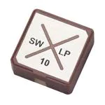
Part No.
:
SWLP.2450.10.4.A.02
Product Name
:
10mm Surface Mount 2.4 GHz Patch Antenna
Feature
:
2400 MHz to 2500 MHz SMT Ceramic Patch Antenna
Best solution for Bluetooth LE Wearable Applications
Works equally well on WIFI/WLAN/ISM/ZigBee
10*10*4mm
Tuned on a 12*16mm ground plane
Linearly Polarized
Patent Pending
RoHS Compliant
SPE-15-8-009/B/WY
Page 1 of 17
�1. Introduction
The SWLP.2450.10.4.A.02 patent pending 10mm SMT ceramic patch antenna is a
breakthrough antenna in terms of size and performance. The smallest 2.4GHz patch
available worldwide, it is ideally suited for 2.4 GHz applications such as Bluetooth LE,
Wi-Fi, ISM, and ZigBee. It was developed specifically for Bluetooth LE wearable
applications to work directly on ground (except for feed area) and over metal, device
environments which traditional chip antennas cannot operate in. The antenna also
does not need ground plane clearance around it (except for feed area). It provides
omni-directional coverage similar to chip antennas on small boards.
The antenna exhibits 24.8% efficiency on a 12*16mm ground plane at 2455 MHz. If
utilized on a 50*50 ground plane, efficiency will improve to 40% at 2455MHz.
Typical applications are:
* Wearables
* Tablets
* Hand-held devices
* USB dongles
* Smart home applications
The SWLP.2450.10.4.A.02 can be placed in any position on the device ground plane.
Like all small antennas, frequency detuning or efficiency change can occur due to
surrounding components and enclosure housing. Larger ground-planes increase peak
gain and efficiency. Taoglas helps customers fine tune the antenna for optimal
performance through matching, correct board layout, transmission line design, and if
necessary, custom antenna tuning for a MOQ.
Many module manufacturers specify peak gain limits for any antennas that are to be
connected to that module. Those peak gain limits are based on free-space conditions.
SPE-15-8-009/B/WY
Page 2 of 17
�In practice, the peak gain of an antenna tested in free-space can degrade by at least
1 or 2dBi when put inside a device. So ideally you should go for a slightly higher peak
gain antenna than mentioned on the module specification to compensate for this
effect, giving you better performance.
Upon testing of any of our antennas with your device and a selection of appropriate
layout, integration technique, or cable, Taoglas can make sure any of our antennas’
peak gain will be below the peak gain limits. Taoglas can then issue a specification
and/or report for the selected antenna in your device that will clearly show it
complying with the peak gain limits, so you can be assured you are meeting regulatory
requirements for that module.
For example, a module manufacturer may state that the antenna must have less than
2dBi peak gain, but you don’t need to select an embedded antenna that has a peak
gain of less than 2dBi in free-space. This will give you a less optimized solution. It is
better to go for a slightly higher free-space peak gain of 3dBi or more if available. Once
that antenna gets integrated into your device, performance will degrade below this
2dBi peak gain due to the effects of GND plane, surrounding components, and device
housing. If you want to be absolutely sure, contact Taoglas and we will test. Choosing
a Taoglas antenna with a higher peak gain than what is specified by the module
manufacturer and enlisting our help will ensure you are getting the best performance
possible without exceeding the peak gain limits.
Contact your regional Taoglas sales office for support.
SPE-15-8-009/B/WY
Page 3 of 17
�2. Specification Table
ELECTRICAL
Frequency Range
2400 MHz to 2500 MHz
Efficiency
24.80% @2455 MHz,
Edge 10.42% @2400 MHz, 11.40% @2500 MHz
Average Gain
-6 dBi @2450 MHz
VSWR
3 max @ Center Frequency
Peak Gain
-1.0 dBi typ.
Polarization
Linear
Impedance
50 Ohm
MECHANICAL
Dimensions
10mm X 10mm X 4mm
Weight
3.1 g
ENVIRONMENTAL RATINGS
Operating Temperature
-40∘C to + 105∘C
Storage Temperature
-40∘C to + 105∘C
*All tests done on a 12*16 mm ground plane. Antenna performance will vary
depending on ground-plane dimensions and housing.
Figure 1 – Antenna on Evaluation Board, Top View (left) and Bottom View (right)
SPE-15-8-009/B/WY
Page 4 of 17
�3. Antenna Characteristics
3.1 Return Loss
3.2 Efficiency
SPE-15-8-009/B/WY
Page 5 of 17
�3.3 Average Gain
3.4 Peak Gain
SPE-15-8-009/B/WY
Page 6 of 17
�4. Antenna Radiation Patterns
4.1 Test Setup
The antenna radiation pattern measurement setup is shown below
Y
X
Z
SPE-15-8-009/B/WY
Page 7 of 17
�4.2 Antenna Radiation Patterns
4.2.1 3D Radiation Pattern at 2450MHz
4.2.2 XY-Plane
X
Y
SPE-15-8-009/B/WY
Page 8 of 17
�4.2.3 XZ-Plane
Z
X
4.2.4 YZ-Plane
Z
Y
SPE-15-8-009/B/WY
Page 9 of 17
�5. Mechanical Drawing
5.1 Patch
Unit:mm
5.2 Evaluation Board Dimensions
Unit:mm
SPE-15-8-009/B/WY
Page 10 of 17
�6. Footprint
6.1 Top Copper
SPE-15-8-009/B/WY
Page 11 of 17
�6.2 Top Solder Paste
SPE-15-8-009/B/WY
Page 12 of 17
�6.3 Top Solder Mask
SPE-15-8-009/B/WY
Page 13 of 17
�6.4 Composite Diagram
SPE-15-8-009/B/WY
Page 14 of 17
�7. Packaging
SPE-15-8-009/B/WY
Page 15 of 17
�SPE-15-8-009/B/WY
Page 16 of 17
�8. Recommended Reflow Temperature Profile
The SWLP.10 can be assembled following Pb-free assembly. According to the Standard
IPC/JEDEC J-STD-020C, the temperature profile suggested is as follows:
Phase
PREHEAT
RAMP-UP
REFLOW
PEAK
RAMP-DOWN
Profile Features
Pb-Free Assembly (SnAgCu)
Temperature Min(Tsmin)
150°C
Temperature Max(Tsmax)
200°C
Time(ts) from (Tsmin to Tsmax)
60-120 seconds
Avg. Ramp-up Rate (Tsmax to TP)
3°C/second(max)
Temperature(TL)
217°C
Total Time above TL (tL)
30-100 seconds
Temperature(TP)
260°C
Time(tp)
15-25 seconds
Rate
6°C/second(max)
Time from 25°C to Peak Temperature
8 minutes max.
Composition of solder paste
96.5Sn/3Ag/0.5Cu
Solder Paste Model
SHENMAO PF606-P26
Soldering condition: Apply preheating at 120°C for 2-3 minutes. Finish soldering for each
terminal within 3 seconds. If soldering iron temperature over270°C±10°C for 3 seconds, it may
cause component surface peeling or damage.
SPE-15-8-009/B/WY
Page 17 of 17
�
SWLP.2450.10.4.A.02 价格&库存
很抱歉,暂时无法提供与“SWLP.2450.10.4.A.02”相匹配的价格&库存,您可以联系我们找货
免费人工找货- 国内价格 香港价格
- 500+43.08170500+5.21299
- 1000+40.693031000+4.92396
- 国内价格 香港价格
- 1+74.661311+9.03420
- 100+66.61269100+8.06030


 工商网监
湘ICP备2023018690号
工商网监
湘ICP备2023018690号
