SPECIFICATION
Part No.
:
HLA.01
Product Name
:
5150-5900 MHz Ceramic Loop antenna
WLAN/ Wi-Fi/ HDMI
Feature
:
3.2mm *1.6mm * 0.5mm
Low profile
Peak gain 2.1dBi
65%+ Efficiency Typical
Compact Size
RoHS Compliant
HLAD.01 EVB Board
Bottom
Top
SPE-12-8-116/B/SS
Page 1 of 19
�1. Introduction
The HLA.01 5150-5900 MHz ceramic chip antenna is specifically designed for
Wi-Fi/ WHDMI applications where high data throughput is needed. It is a high
efficiency miniature SMD edge mounted ceramic antenna with minimum
footprint requirement. This ceramic chip antenna uses the main PCB as its
ground plane, thereby increasing antenna efficiency. It is tuned for different
PCB sizes by simply changing the value of the matching circuit. The HLA.01
with dimension of 3.2mm *1.6mm * 0.5mm, is one of the smallest antennas
available worldwide. This antenna is delivered on tape and reel.
Many module manufacturers specify peak gain limits for any antennas that are
to be connected to that module. Those peak gain limits are based on free-space
conditions. In practice, the peak gain of an antenna tested in free-space can
degrade by at least 1 or 2dBi when put inside a device. So ideally you should go
for a slightly higher peak gain antenna than mentioned on the module
specification to compensate for this effect, giving you better performance.
Upon testing of any of our antennas with your device and a selection of
appropriate layout, integration technique, or cable, Taoglas can make sure any
of our antennas’ peak gain will be below the peak gain limits. Taoglas can then
issue a specification and/or report for the selected antenna in your device that
will clearly show it complying with the peak gain limits, so you can be assured
you are meeting regulatory requirements for that module.
For example, a module manufacturer may state that the antenna must have
less than 2dBi peak gain, but you don’t need to select an embedded antenna
that has a peak gain of less than 2dBi in free-space. This will give you a less
optimized solution. It is better to go for a slightly higher free-space peak gain
SPE-12-8-116/B/SS
Page 2 of 19
�of 3dBi or more if available. Once that antenna gets integrated into your device,
performance will degrade below this 2dBi peak gain due to the effects of GND
plane, surrounding components, and device housing. If you want to be
absolutely sure, contact Taoglas and we will test. Choosing a Taoglas antenna
with a higher peak gain than what is specified by the module manufacturer and
enlisting our help will ensure you are getting the best performance possible
without exceeding the peak gain limits.
Applications
IEEE802.11a (5150-5900 MHz)
WHDMI PCMCIA cards or Wireless USB dongles
2. Specification Table
Electrical
Center Frequency (MHz)
5500
SPE-12-8-116/B/SS
Page 3 of 19
�Bandwidth (MHz)
524
Peak Gain (dBi)
2.1 (typical)
Efficiency (%)
65 (typical)
VSWR
2 max.
Impedance (Ω)
50
Polarization
Linear
Radiation Pattern
Omni
Input Power(W)
50
MECHANICAL
Dimensions (mm)
3.2 x 1.6 x 0.5
Ground plane (mm)
80x40
Material
AS 6
ENVIRONMENTAL
Temperature Range
Temperature Coefficient of
Frequency (ppm/°C)
Humidity
-40°C to 85°C
0±20 max. (@-40°C to 85°C)
Non-condensing 65°C 95% RH
SPE-12-8-116/B/SS
Page 4 of 19
�3. Return Loss
SPE-12-8-116/B/SS
Page 5 of 19
�4. Smith Chart
SPE-12-8-116/B/SS
Page 6 of 19
�5. Efficiency
SPE-12-8-116/B/SS
Page 7 of 19
�6. Antenna Radiation Patterns
Y
X
Z
6.1 3D Gain pattern @ 5150 MHz
SPE-12-8-116/B/SS
Page 8 of 19
�SPE-12-8-116/B/SS
Page 9 of 19
�6.2 3D Gain pattern @ 5350 MHz
SPE-12-8-116/B/SS
Page 10 of 19
�6.3 3D Gain pattern @ 5700 MHz
SPE-12-8-116/B/SS
Page 11 of 19
�SPE-12-8-116/B/SS
Page 12 of 19
�6.4 3D Gain pattern @ 5850 MHz
SPE-12-8-116/B/SS
Page 13 of 19
�SPE-12-8-116/B/SS
Page 14 of 19
�7. Mechanical Drawing
SPE-12-8-116/B/SS
Page 15 of 19
�8. Layout Guide
Solder Land Pattern:
SPE-12-8-116/B/SS
Page 16 of 19
�9. Frequency tuning
Antenna tuning scenario:
Matching circuit: (Center frequency is 5500MHz at 80x40mm ground plane)
SPE-12-8-116/B/SS
Page 17 of 19
�10. Soldering Conditions
Typical Soldering profile for lead-free process:
SPE-12-8-116/B/SS
Page 18 of 19
�11. Packing
Quantity: 6000pcs/ Reel
Plastic tape:
Tape Dimensions (unit: mm)
Feature
Specification
Tolerance
W
12.00
±0.30
P
8.00
±0.10
E
1.75
±0.10
F
5.50
±0.10
Feature
Specification
Tolerance
P2
2.00
±0.10
Ao
1.90
+0.20
D
1.50
+0.10 / -0.00
Bo
3.50
-0.10
D1
-
±0.10
Ko
0.60
±0.05
Po
4.00
±0.10
t
0.30
±0.05
10Po
40.00
±0.20
Pocket Dimensions (unit: mm)
1. Cumulative tolerance of 10 pocket hole pitch: ±0.20mm
2. Carrier camber not to exceed 1mm in 250mm
3. Ao and Bo measured on a plane above the inside bottom of the pocket
4. Ko measured from a plane on the inside bottom of the pocket to the top surface
of the carrier
5. All dimensions meet EIA-481-B requirements
6. Material – Clear non Anti-Static Polystyrene, Black Conductive Polystyrene
SPE-12-8-116/B/SS
Page 19 of 19
�
很抱歉,暂时无法提供与“HLAD.01”相匹配的价格&库存,您可以联系我们找货
免费人工找货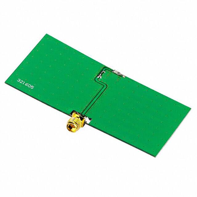


 工商网监
湘ICP备2023018690号
工商网监
湘ICP备2023018690号
