�CONTENTS
CHAPTER 1
INTRODUCTION ........................................................................................................... 3
1.1 The Package Contents ................................................................................................................................ 3
1.2 Assemble LT24 with DE0-Nano ................................................................................................................. 4
1.3 Connectivity ............................................................................................................................................... 5
1.4 Getting Help ............................................................................................................................................... 7
CHAPTER 2
ARCHITECTURE OF LT24 ............................................................................................ 8
2.1 Features....................................................................................................................................................... 8
2.2 Layout and Block Diagram......................................................................................................................... 8
CHAPTER 3
USING THE LT24 ........................................................................................................ 10
3.1 Pin Definition of 2x20 GPIO Connector .................................................................................................. 10
3.2 Using LCD................................................................................................................................................ 12
3.3 Using Touch.............................................................................................................................................. 13
CHAPTER 4
PAINTER DEMONSTRATION ....................................................................................... 15
4.1 Description ............................................................................................................................................... 15
4.2 System Description ................................................................................................................................... 16
4.3 LT24 LCD Controller ............................................................................................................................... 17
4.4 Setup Painter Demo on Terasic DE2-115 FPGA Board ........................................................................... 17
4.5 Painter Demo for Other Terasic FPGA Mainboards ................................................................................. 18
CHAPTER 5
LT24 DISPLAY ............................................................................................................ 19
5.1 Description ............................................................................................................................................... 19
5.2 System Description ................................................................................................................................... 20
5.3 LT24 LCD Initialization ........................................................................................................................... 20
5.4 Setup Demo on Terasic DE0-Nano FPGA Board ..................................................................................... 21
5.5 LT24_Display Demo for Other Terasic FPGA Mainboards ..................................................................... 22
CHAPTER 6
APPENDIX .................................................................................................................. 23
LT24 User Manual
1
www.terasic.com
June 1, 2015
�6.1 Revision History ....................................................................................................................................... 23
6.2 Copyright Statement ................................................................................................................................. 23
LT24 User Manual
2
www.terasic.com
June 1, 2015
�Chapter 1
Introduction
The Terasic LT24 is a 2.4” LCD touch module with 240(H) x 320(V) display resolution. It can be
bundled with various Terasic FPGA development boards through the 2x20 GPIO interface. The
LT24 is powered directly from the FPGA mainboard. It doesn’t require any power adaptor. The kit
contains complete reference design and source code for the Painter application. This chapter
provides the key information about the kit.
1.1 The Package Contents
The LT24 kit comes with the following items:
LT24 touch LCD module
Two silicon footstands
Two screw nuts
Two hexagon copper pillars
CD download guide
The system CD contains technical documents of LT24 kit, which include component datasheets,
demonstrations, schematic and user manual. Users can download the CD from the link below:
http://cd-lt24.terasic.com
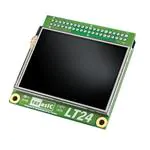
Figure 1-1 shows the contents of LT24 kit.
Figure 1-1 Contents of LT24 kit
LT24 User Manual
3
www.terasic.com
June 1, 2015
�1.2 Assemble LT24 with DE0-Nano
There are two holes reserved on the LT24 for the screws to stabilize the installation with other
mainboards by adding copper pillars onto them. The following steps take DE0-Nano as an example
to demonstrate the installation with the copper pillars.
1.
Install the screw nuts from top to the bottom of screw holes reserved on the LT24. Install the
hexagon copper pillars and make sure then are tightened up, as shown in Figure 1-2.
Figure 1-2 Install the hexagon copper pillars
2.
Cover the two copper pillars of LT24 with two silicon footstands, as shown in Figure 1-3. This
procedure can be skipped if the LT24 is assembled with DE0-Nano.
Figure 1-3 Install the footstand
3.
Connect the LT24 to the GPIO header of DE0-Nano, as shown in Figure 1-4.
LT24 User Manual
4
www.terasic.com
June 1, 2015
�Figure 1-4 LT24 Assembled with DE0-Nano
1.3 Connectivity
Figure 1-5, Figure 1-6, Figure 1-7 and Figure 1-8 below show the connectivity of LT24 to
DE0-Nano, DE1-SoC, DE2-115 and C5G(Cyclone V GX Starter Kit), respectively. The LT24 is
powered from FPGA mainboard. It is not necessary to connect the LT24 with a power adaptor.
Figure 1-5 LT24 with DE0-Nano
LT24 User Manual
5
www.terasic.com
June 1, 2015
�Figure 1-6 LT24 with DE1-SoC
Figure 1-7 LT24 with DE2-115
Figure 1-8 LT24 with C5G (Cyclone V GX Starter Kit)
LT24 User Manual
6
www.terasic.com
June 1, 2015
�1.4 Getting Help
Here is the information to get help if you encounter any problem:
Office Hours: 9:00 a.m. to 6:00 p.m. (GMT +8)
Telephone: +886-3-575-0880
Email: support@terasic.com
LT24 User Manual
7
www.terasic.com
June 1, 2015
�Chapter 2
Architecture of LT24
This chapter lists the features and describes the architecture of 2.4” LCD touch module (LT24).
2.1 Features
The key features of this module are listed below:
240(H) x 320 (V) pixel resolution LCD with 65K RGB color
Single resistive touch
2x20 GPIO interface
2.2 Layout and Block Diagram
Component and Layout
The top view of LT24 is shown in Figure 2-1.
Figure 2-1 Top view of LT24
The bottom view of LT24 is shown in Figure 2-2. It depicts the layout and indicates the locations of
connectors and key components.
LT24 User Manual
8
www.terasic.com
June 1, 2015
�Figure 2-2 Bottom view of LT24 module
Block Diagram
Figure 2-3 shows the block diagram of LT24. An ADC chip is used to handle the 4-wire
touchscreen.
Figure 2-3 Block diagram of LT24
LT24 User Manual
9
www.terasic.com
June 1, 2015
�Chapter 3
Using the LT24
This chapter provides information on how to control the hardware of 2.4” LCD touch module
(LT24), including the definition of 2x20 GPIO interface, LCD control, and touch control signals.
3.1 Pin Definition of 2x20 GPIO Connector
The 2x20 GPIO female connector on LT24 connects directly to the 2x20 GPIO male connector on
Terasic FPGA development boards. Figure 3-1 illustrates the signal names of 2x20 GPIO Header.
Figure 3-1 Signal names of 2x20 GPIO connector
LT24 User Manual
10
www.terasic.com
June 1, 2015
�Table 3-1 shows the LT24 pin assignments for the 2x20 GPIO pins in Quartus II.
Table 3-1 LT24 Pin Assignments of 2x20 GPIO in Quartus II
Pin
Numbers
Pin Name
Direction
IO Standard
1
2
3
4
5
6
7
8
9
10
11
12
13
14
15
16
17
18
19
20
21
22
23
24
25
26
27
28
29
30
31
32
33
34
35
36
37
ADC_PENIRQ_N
ADC_DOUNT
ADC_BUSY
ADC_DIN
ADC_DCLK
D[3]
D[2]
D[1]
D[0]
RD_N
WR_N
RS
D[4]
D[5]
D[6]
D[7]
D[8]
D[9]
D[10]
D[11]
D[12]
D[13]
D[14]
D[15]
CS_N
-
Input
Input
Input
Output
Output
Output
Output
Output
Output
Output
Output
Output
Output
Output
Output
Output
Output
Output
Output
Output
Output
Output
Output
Output
Output
-
3.3-V LVTTL
3.3-V LVTTL
3.3-V LVTTL
3.3-V LVTTL
3.3-V LVTTL
3.3-V LVTTL
3.3-V LVTTL
3.3-V LVTTL
3.3-V LVTTL
3.3-V LVTTL
3.3-V LVTTL
3.3-V LVTTL
3.3-V LVTTL
3.3-V LVTTL
3.3-V LVTTL
3.3-V LVTTL
3.3-V LVTTL
3.3-V LVTTL
3.3-V LVTTL
3.3-V LVTTL
3.3-V LVTTL
3.3-V LVTTL
3.3-V LVTTL
3.3-V LVTTL
3.3-V LVTTL
-
LT24 User Manual
11
www.terasic.com
June 1, 2015
�38
39
40
RESET_N
ADC_CS_N
LCD_ON
Output
Output
Output
3.3-V LVTTL
3.3-V LVTTL
3.3-V LVTTL
3.2 Using LCD
The LCD features 240(H) x 320(V) pixel resolution. The ILI9341 LCD driver is used to drive the
LCD display. The 65K-Color, RGB 5-6-5 bits input data based on 8080-system 16-bit parallel bus
interface of ILI9341 is used on the LT24. For further information, please refer to the section 7.6.5
“16-bit Parallel MCU Interface” of ILI9341 datasheet in the LT24 System CD. Figure 3-2 shows
the signals connected between the ILI9341 and the FPGA.
Figure 3-2 Signals of LCD driver connected to FPGA
CSX is a low-active chip select pin. D/CX is Data or Command selection pin. When D/CX = 1,
data selected. When D/CX = 0, command is selected. WRX is a write signal and writes data at the
rising edge. RDX is a read signal and MCU read data at the rising edge. D[15:0] is data bus. Figure
3-3 shows pixel data transfer format. The D0~D7 are used to translate command to ILI9341 in the
command mode (D/CX=0). The D0~D15 are used to translate the RGB data to ILI9341 in data
mode (D/CX=1).
LT24 User Manual
12
www.terasic.com
June 1, 2015
�Figure 3-3 65K-Color, 5-6-5 bits pixel data format
3.3 Using Touch
The AD7843 from Analog Device is a 12-bit analog-to-digital converter (ADC) used to digitize the
touch points from the touch panel of LT24 into the corresponding X/Y coordinates on LT24.
To obtain the coordinates from the ADC, users need to monitor the interrupt signal
ADC_PENIRQ_n coming out of the ADC first. The ADC_PENIRQ_n output remains high in
normal condition by connecting a pull high resistor to it. When the touch screen connected to the
ADC is trigger via a pen or finger, the ADC_PENIRQ_n output goes low and it initiates an interrupt
to FPGA, which instructs a control word to be written to the ADC via the serial port interface.
The control word provided to the ADC via the DIN pin is shown in Table 3-2. It controls the
conversion start, channel addressing, ADC conversion resolution, configuration, and power-down of
the ADC. The detailed information about the order and description of these control bits can be
found in the datasheet from the DATASHEET folder in the LT24 System CD.
Table 3-2 Control Register Bit Function Description
MSB
LSB
S
A2
A1
A0
MODE SER / DEF PD1
PD0
Bit
7
Mnemonic Comment
Start Bit. The control word starts with the first high
bit on DIN. A new control word can start every 15th
S
DCLK cycle when in the 12-bit conversion mode, or
every 11th DCLK cycle when in 8-bit conversion
mode.
LT24 User Manual
13
www.terasic.com
June 1, 2015
�Channel Select Bits. These three address bits, along
6-4
3
A2-A0
MODE
2
SER / DEF
1,0
PD1,PD0
with the
SER / DEF
bit, control the setting of the
multiplexer input,
switches, and reference inputs.
12-Bit/8-Bit Conversion Select Bit. This bit controls
the resolution of the following conversion. With 0 in
this bit, the
conversion has a 12-bit resolution, or with 1 in this
bit, the conversion has a 8-bit resolution.
Single-Ended/Differential Reference Select Bit.
Along with Bits A2–A0, this bit controls the setting
of the multiplexer
input, switches, and reference inputs.
Power Management Bits. These two bits decode the
power-down mode of the AD7843.
Figure 3-4 shows the typical operation of serial interface of AD7843 ADC. The serial clock
provides the conversion clock and controls the information transfer to and from the ADC. A
complete conversion can be achieved after 24 ADC_DCLK cycles. The detailed behavior of serial
port interface can be found in the datasheet of AD7843 ADC.
Figure 3-4 Conversion timing of serial port interface
LT24 User Manual
14
www.terasic.com
June 1, 2015
�Chapter 4
Painter Demonstration
This chapter shows how to implement the painter demonstration on LT24. The demo is designed in
Qsys and running by Nios II processor. Altera SPI IP in Qsys is used to retrieve the touch
information from the touch screen. Terasic custom display component in Qsys is used to display
image on the 2.4” LCD. This demo requires the following hardware:
Terasic FPGA board
LT24 LCD touch module
4.1 Description
Figure 4-1 shows the Graphical User Interface (GUI) of Painter demo. The GUI is composed by
three sections: Painting Area, Clear Button, and Color Palette. Users can select a color from the
color palette and start drawing in the paint area. Click the “Clear” button to clear the painting area.
Figure 4-1 GUI of Painter demo
Figure 4-2 displays the painting on the canvas area.
LT24 User Manual
15
www.terasic.com
June 1, 2015
�Figure 4-2 Painting demo running on LT24 with DE2-115
4.2 System Description
Figure 4-3 shows the system block diagram of Painter demonstration. Terasic custom Qsys
component - LT24 LCD controller is used to display 240(H) x 320(V) image. Its source code is
located in the “/ip/LT24_Controller” folder of Painter demo project. Qsys built-in SPI controller is
used to communicate with the AD7843 ADC via SPI interface to retrieve data from the touch screen.
The Nios II program handles touch event and image display. It is stored in either on-chip memory or
external memory. The LCD module should be initialized before sending image data to the LCD for
image display.
Figure 4-3 System block diagram of Painter demonstration
LT24 User Manual
16
www.terasic.com
June 1, 2015
�4.3 LT24 LCD Controller
The LT24 LCD controller is a custom Qsys component developed by Teraisc. Its source code is
located in the “/ip/LT24_Controller” folder of Painter demo project. Table 4-1 shows the register
definition of LT24 LCD controller. The controller base address is defined as LT24_BASE in the
Nios II program. The function of writing a control command to the LCD driver is IOWR(LT24_
BASE, 0x00, CommandValue). The function of writing data to the LCD driver is
IOWR(LT24_BASE, 0x01, DataValue).
Table 4-1 Register Definition and Offset for the Painter Demonstration
Byte Offset
Register Name Description
0
Control Port
4
Data Port
Write control command to the LCD
driver
Write data to the LCD driver
4.4 Setup Painter Demo on Terasic DE2-115 FPGA Board
This section shows how to setup the Painter demo on the Terasic DE2-115 FPGA board.
Hardware Setup
Figure 4-4 shows the demo setup of LT24 with DE2-115 FPGA mainboard. The LT24 should be
installed on the GPIO expansion header of DE2-115.
Figure 4-4 Hardware setup of LT24 with DE2-115
Execute Demonstration
Please follow the procedures below to setup the demonstration:
LT24 User Manual
17
www.terasic.com
June 1, 2015
�1. Power off the DE2-115.
2. Mount the LT24 onto the 2x20 GPIO 0 expansion header of DE2-115.
3. Connect the USB-Blaster USB port of DE2-115 to the USB port of host PC with a USB
cable.
4. Power on the DE2-115 FPGA board.
5. Both Quartus II and USB-Blaster II driver must be installed on the host PC.
6. Copy the folder Demonstrations//DE2_115_LT24_PAINTER/demo_batch from the LT24
System CD to the host PC and execute “DE2_115.bat”.
7. The Painter demo should be up and running on the LCD.
Source Code
The source code of Quartus project for the Painter demo with DE2-115 board is available in the
“Demonstrations\DE2_115_LT24_PAINTER” folder from the LT24 System CD. The Eclipse Nios
II project workspace is located in the “software” sub-folder under the Quartus project folder.
4.5 Painter Demo for Other Terasic FPGA Mainboards
The LT24 System CD also contains Quartus projects for other FPGA mainboards. The locations of
source code for the Quartus projects with other Tearsic FPGA mainboards are shown in Table 4-2.
For DE1-SoC, two Quartus projects are included in the Ssytem CD. The difference between these
two projects is the memory where the Nios II program is running on. For Cyclone V GX Starter kit,
there are two Quartus projects included in the LT24 System CD. The difference between these
projects is also the memory where the Nios II program is running on.
To execute the demo on DE0-Nano, please connect the LT24 to the GPIO-1 expansion header of
DE0-Nano. To execute the demo on DE1-SoC, please connect the LT24 to the GPIO-1 expansion
header of DE1-SoC. DE0_Nano_SoC_OCRM_LT24_Painter is built by Quartus 14.1, and the
other Quartus projects are built by Quartus II v13.1.
Table 4-2 Locations of Source Code for the Painter Demo with Other FPGA Boards
FPGA Board
Memory Location
DE0-Nano
SDRAM Demonstrations\DE0_Nano_SDRAM_LT24_PAINTER
DE2-115
On-chip Demonstrations\DE2_115_OnChipMemory_LT24_PAINTER
DE1-SoC
SDRAM Demonstrations\DE1_SOC_SDRAM_LT24_PAINTER
DE1-SoC
On-chip Demonstrations\DE1_SOC_OnChipMemory_LT24_PAINTER
Cyclone V GX Starter Kit On-chip Demonstrations\C5G_OnChipMemory_LT24_PAINTER
Cyclone V GX Starter Kit SRAM Demonstrations\C5G_SRAM_LT24_PAINTER
DE0-Nano-Soc
On-Chip DE0_Nano_SoC_OCRAM_LT24_Painter
DE2
SDRAM DE2_SDRAM_LT24_Painter
LT24 User Manual
18
www.terasic.com
June 1, 2015
�Chapter 5
LT24_Display
This chapter shows how to implement the lt24-display demonstration on LT24. This design is only
RTL code, There is not CPU, Memory. This demo requires the following hardware:
Terasic FPGA board
LT24 LCD touch module
5.1 Description
shows the Graphical User Interface (GUI) of LT24-Display demo. LT24-Display this
demo is mainly on the LT24 can respectively show the R, G, B three color base map, as well as a
simple line drawing functions. Place in the bottom three colors can click to switch between different
color base map, there is a hidden feature, click on the top right corner, you can clear the lines
depicted.
Figure 5-1
Figure 5-1 GUI of LT24-Display demo
LT24 User Manual
19
www.terasic.com
June 1, 2015
�Figure 5-2 Painting demo running on LT24 with DE0-Nano
5.2 System Description
shows the system block diagram of LT24-Display demonstration. LT24_Display of RTL
(Verilog) code on the demo project of "/ ip / lt24_display" folder. As Figure 5-3 shown, lt24_display
the top module - lt24_display.v contains four block. Pat_update.v is used with Touch (AD7843)
connection, pat_update module will receive the AD7843 in touch information (x, y coordinates),
and then converted into the corresponding action, this action triggers to the LCD display module
generates commands, and command again through cmd2lcd module to convert LCD panel (ILI9341)
can accept signals. The last timer module has only one function - to produce a 33ms signal, which is
used to make a long delay of the clock, such as LCD during the initial stage will need ms delay.
Figure 5-3
Figure 5-3 System block diagram of LT24-Display demonstration
5.3 LT24 LCD Initialization
The LCD of LT24 is needed before the initial use of. Because LT24-Display of pure RTL code
design, there is no CPU, so can not be used to initial LCD mode CPU-base system (set registers to
LT24 User Manual
20
www.terasic.com
June 1, 2015
�complete the process), as used herein, FSM (Final State Machine) to set the initial flow, refer to
"/ip/lt24_display/display.v" file, in initail LCD wait pat_update event after entering the loop. There
CPU systems are more flexible, we have to change the process, C-code in order to change what you
can; but the reaction time is slower, received from the AD7843 to output to the LCD touch response
time will be longer. Compared to pure RTL code of the design, although the initial process because
of the limited FSM relatively less flexible, but because the relationship between the hardware
processing, AD7843 to LCD's response time faster.
5.4 Setup Demo on Terasic DE0-Nano FPGA Board
This section shows how to setup the LT24-Display demo on the Terasic DE0-Nano FPGA board.
Hardware Setup
錯誤! 找不到參照來源。 shows the demo setup of LT24 with DE0-Nano FPGA mainboard. The
LT24 should be installed on the GPIO_1 expansion header of DE0-Nano.
Execute Demonstration
Please follow the procedures below to setup the demonstration:
1. Power off the DE0-Nano (disconnect USB cable).
2. Mount the LT24 onto the 2x20 GPIO 1 expansion header of DE0-Nano.
3. Connect the USB-Blaster USB port of DE0-Nano to the USB port of host PC with a USB
LT24 User Manual
21
www.terasic.com
June 1, 2015
�cable (Power on).
4. Both Quartus II and USB-Blaster II driver must be installed on the host PC.
5. Copy the folder Demonstrations//DE0_Nano_LT24_Display/demo_batch from the LT24
System CD to the host PC and execute “test.bat”.
6. The RGB-Display demo should be up and running on the LCD.
Source Code
The source code of Quartus project for the LT24-display demo with DE0-Nano board is available in
the “Demonstrations\DE0_nano_LT24_display” folder from the LT24 System CD.
5.5 Display Demo for Other Terasic FPGA Mainboards
The LT24 System CD also contains Quartus projects for other FPGA mainboards. The locations of
source code for the Quartus projects with other Tearsic FPGA mainboards are shown in Table 5-1.
To execute the demo on DE0-Nano, please connect the LT24 to the GPIO-1 expansion header of
DE0-Nano. To execute the demo on DE2-115, please connect the LT24 to the GPIO expansion
header of DE2-115. To execute the demo on DE1-SoC, please connect the LT24 to the GPIO-1
expansion header of DE1-SoC. To execute the demo on C5G, please connect the LT24 to the GPIO
expansion header of C5G. All the Quartus projects are built in Quartus II v13.1.
Table 5-1 Locations of Source Code for the LT24-Display Demo with Other FPGA Boards
FPGA Board
Location
DE0-Nano
DE2-115
DE1-SoC
Cyclone V GX Starter Kit
Demonstrations\DE0_Nano_ LT24_Display
Demonstrations\DE2_115_ LT24_ Display
Demonstrations\DE1_SOC_ LT24_ Display
Demonstrations\C5G_ LT24_ Display
LT24 User Manual
22
www.terasic.com
June 1, 2015
�Chapter 6
Appendix
6.1
Revision Histor y
Version
Change Log
V1.0
V1.0.1
Initial Version (Preliminary)
Add painter demo path for de0-nano-soc and DE2.
6.2
Copyright Statement
Copyright © 2014 Terasic Technologies. All rights reserved.
We will continue to provide examples and lab exercises on our LT24 webpage. Please visit
http://lt24.terasic.com for more information.
LT24 User Manual
23
www.terasic.com
June 1, 2015
�


 工商网监
湘ICP备2023018690号
工商网监
湘ICP备2023018690号
