VS1053b Datasheet
VS1053b Ogg Vorbis/MP3/AAC/WMA/FLAC/
MIDI AUDIO CODEC CIRCUIT
Features
Description
VS1053b is an Ogg Vorbis/MP3/AAC/WMA/
• Decodes
FLAC/WAVMIDI audio decoder as well as an
Ogg Vorbis;
PCM/IMA ADPCM/Ogg Vorbis encoder on a
MP3 = MPEG 1 & 2 audio layer III (CBR
single chip. It contains a high-performance,
+VBR +ABR);
proprietary low-power DSP processor core
MP1/MP2 = layers I & II optional;
VS_DSP4 , data memory, 16 KiB instruction
MPEG4 / 2 AAC-LC(+PNS),
RAM and 0.5+ KiB data RAM for user appliHE-AAC v2 (Level 3) (SBR + PS);
WMA 4.0/4.1/7/8/9 all profiles (5-384 kbps); cations running simultaneously with any builtin decoder, serial control and input data inGeneral MIDI 1 / SP-MIDI format 0 files;
terfaces, upto 8 general purpose I/O pins, an
FLAC with software plugin;
UART, as well as a high-quality variable-sampleWAV (PCM + IMA ADPCM)
rate stereo ADC (mic, line, line + mic or 2×line)
• Encodes Ogg Vorbis w/ software plugin
and stereo DAC, followed by an earphone am• Encodes stereo IMA ADPCM / PCM
plifier and a common voltage buffer.
• Streaming support for MP3 and WAV
• EarSpeaker Spatial Processing
VS1053b receives its input bitstream through
• Bass and treble controls
a serial input bus, which it listens to as a
• Operates with a single 12..13 MHz clock
system slave. The input stream is decoded
• Can also be used with a 24..26 MHz clock and passed through a digital volume control
to an 18-bit oversampling, multi-bit, sigma• Internal PLL clock multiplier
delta DAC. The decoding is controlled via a
• Low-power operation
serial control bus. In addition to the basic de• High-quality on-chip stereo DAC with no
coding, it is possible to add application spephase error between channels
cific features, like DSP effects, to the user
• Zero-cross detection for smooth volume
RAM memory.
change
• Stereo earphone driver capable of drivOptional factory-programmable unique chip
ing a 30 Ω load
ID provides basis for digital rights manage• Quiet power-on and power-off
ment or unit identification features.
• I2S interface for external DAC
• Separate voltages for analog, digital, I/O
• On-chip RAM for user code and data
• Serial control and data interfaces
• Can be used as a slave co-processor
• SPI flash boot for special applications
• UART for debugging purposes
• New functions may be added with software and upto 8 GPIO pins
• Lead-free RoHS-compliant package (Green)
Version: 1.20, 2012-12-03
1
�VS1053b Datasheet
CONTENTS
Contents
VS1053
1
Table of Contents
2
List of Figures
5
1 Licenses
6
2 Disclaimer
6
3 Definitions
6
4 Characteristics & Specifications
4.1 Absolute Maximum Ratings . . . . . . . . .
4.2 Recommended Operating Conditions . . . .
4.3 Analog Characteristics . . . . . . . . . . . .
4.4 Power Consumption . . . . . . . . . . . . .
4.5 Digital Characteristics . . . . . . . . . . . . .
4.6 Switching Characteristics - Boot Initialization
.
.
.
.
.
.
7
7
7
8
9
9
9
5 Packages and Pin Descriptions
5.1 Packages . . . . . . . . . . . . . . . . . . . . . . . . . . . . . . . . . . . . . . .
5.1.1 LQFP-48 . . . . . . . . . . . . . . . . . . . . . . . . . . . . . . . . . .
10
10
10
6 Connection Diagram, LQFP-48
13
7 SPI Buses
7.1 SPI Bus Pin Descriptions . . . . . . . . . . . . . . . . . . . . . . . . . . . . . . .
7.1.1 VS10xx Native Modes (New Mode, recommended) . . . . . . . . . .
7.1.2 VS1001 Compatibility Mode (deprecated, do not use in new designs)
7.2 Data Request Pin DREQ . . . . . . . . . . . . . . . . . . . . . . . . . . . . . . .
7.3 Serial Protocol for Serial Data Interface (SPI / SDI) . . . . . . . . . . . . . . . .
7.3.1 SDI in VS10xx Native Modes (New Mode, recommended) . . . . . .
7.3.2 SDI Timing Diagram in VS10xx Native Modes (New Mode) . . . . . .
7.3.3 SDI in VS1001 Compatibility Mode (deprecated, do not use in new
designs) . . . . . . . . . . . . . . . . . . . . . . . . . . . . . . . . . .
7.3.4 Passive SDI Mode (deprecated, do not use in new designs) . . . . .
7.4 Serial Protocol for Serial Command Interface (SPI / SCI) . . . . . . . . . . . . .
7.4.1 SCI Read . . . . . . . . . . . . . . . . . . . . . . . . . . . . . . . . .
7.4.2 SCI Write . . . . . . . . . . . . . . . . . . . . . . . . . . . . . . . . .
7.4.3 SCI Multiple Write . . . . . . . . . . . . . . . . . . . . . . . . . . . . .
7.4.4 SCI Timing Diagram . . . . . . . . . . . . . . . . . . . . . . . . . . .
7.5 SPI Examples with SM_SDINEW and SM_SDISHARED set . . . . . . . . . . .
7.5.1 Two SCI Writes . . . . . . . . . . . . . . . . . . . . . . . . . . . . . .
7.5.2 Two SDI Bytes . . . . . . . . . . . . . . . . . . . . . . . . . . . . . . .
7.5.3 SCI Operation in Middle of Two SDI Bytes . . . . . . . . . . . . . . .
15
15
15
15
16
17
17
18
8 Supported Audio Decoder Formats
8.1 Supported MP3 (MPEG layer III) Formats . . . . . . . . . . . . . . . . . . . . .
8.2 Supported MP2 (MPEG layer II) Formats . . . . . . . . . . . . . . . . . . . . . .
25
25
26
Version: 1.20, 2012-12-03
.
.
.
.
.
.
.
.
.
.
.
.
.
.
.
.
.
.
.
.
.
.
.
.
.
.
.
.
.
.
.
.
.
.
.
.
.
.
.
.
.
.
.
.
.
.
.
.
.
.
.
.
.
.
.
.
.
.
.
.
.
.
.
.
.
.
.
.
.
.
.
.
.
.
.
.
.
.
.
.
.
.
.
.
.
.
.
.
.
.
.
.
.
.
.
.
.
.
.
.
.
.
.
.
.
.
.
.
.
.
.
.
.
.
19
19
20
20
21
21
22
23
23
23
24
2
�VS1053b Datasheet
8.3
8.4
8.5
8.6
8.7
8.8
8.9
Supported MP1 (MPEG layer I) Formats . . . . . . . . . . . . . . .
Supported Ogg Vorbis Formats . . . . . . . . . . . . . . . . . . . .
Supported AAC (ISO/IEC 13818-7 and ISO/IEC 14496-3) Formats
Supported WMA Formats . . . . . . . . . . . . . . . . . . . . . . .
Supported FLAC Formats . . . . . . . . . . . . . . . . . . . . . . .
Supported RIFF WAV Formats . . . . . . . . . . . . . . . . . . . . .
Supported MIDI Formats . . . . . . . . . . . . . . . . . . . . . . . .
9 Functional Description
9.1 Main Features . . . . . . . . . . . . . . . . .
9.2 Data Flow of VS1053b . . . . . . . . . . . .
9.3 EarSpeaker Spatial Processing . . . . . . .
9.4 Serial Data Interface (SDI) . . . . . . . . . .
9.5 Serial Control Interface (SCI) . . . . . . . .
9.6 SCI Registers . . . . . . . . . . . . . . . . .
9.6.1 SCI_MODE (RW) . . . . . . . . .
9.6.2 SCI_STATUS (RW) . . . . . . . .
9.6.3 SCI_BASS (RW) . . . . . . . . .
9.6.4 SCI_CLOCKF (RW) . . . . . . . .
9.6.5 SCI_DECODE_TIME (RW) . . .
9.6.6 SCI_AUDATA (RW) . . . . . . . .
9.6.7 SCI_WRAM (RW) . . . . . . . . .
9.6.8 SCI_WRAMADDR (W) . . . . . .
9.6.9 SCI_HDAT0 and SCI_HDAT1 (R)
9.6.10 SCI_AIADDR (RW) . . . . . . . .
9.6.11 SCI_VOL (RW) . . . . . . . . . .
9.6.12 SCI_AICTRL[x] (RW) . . . . . . .
CONTENTS
.
.
.
.
.
.
.
.
.
.
.
.
.
.
.
.
.
.
.
.
.
.
.
.
.
.
.
.
.
.
.
.
.
.
.
.
.
.
.
.
.
.
.
.
.
.
.
.
.
26
26
27
29
30
30
31
.
.
.
.
.
.
.
.
.
.
.
.
.
.
.
.
.
.
.
.
.
.
.
.
.
.
.
.
.
.
.
.
.
.
.
.
.
.
.
.
.
.
.
.
.
.
.
.
.
.
.
.
.
.
.
.
.
.
.
.
.
.
.
.
.
.
.
.
.
.
.
.
.
.
.
.
.
.
.
.
.
.
.
.
.
.
.
.
.
.
.
.
.
.
.
.
.
.
.
.
.
.
.
.
.
.
.
.
.
.
.
.
.
.
.
.
.
.
.
.
.
.
.
.
.
.
.
.
.
.
.
.
.
.
.
.
.
.
.
.
.
.
.
.
.
.
.
.
.
.
.
.
.
.
.
.
.
.
.
.
.
.
.
.
.
.
.
.
.
.
.
.
.
.
.
.
.
.
.
.
.
.
.
.
.
.
.
.
.
.
.
.
.
.
.
.
.
.
.
.
.
.
.
.
.
.
.
.
.
.
.
.
.
.
.
.
.
.
.
.
.
.
.
.
.
.
.
.
.
.
.
.
.
.
.
.
.
.
.
.
.
.
.
.
.
.
.
.
.
.
.
.
.
.
.
.
.
.
.
.
.
.
.
.
.
.
.
.
.
.
.
.
.
.
.
.
.
.
.
.
.
.
.
.
.
.
.
.
.
.
.
.
.
.
.
.
.
.
.
.
.
.
.
.
.
.
33
33
34
35
36
36
37
38
40
41
42
43
43
43
43
44
46
47
47
10 Operation
10.1 Clocking . . . . . . . . . . . . . . . . . . . . . . . .
10.2 Hardware Reset . . . . . . . . . . . . . . . . . . . .
10.3 Software Reset . . . . . . . . . . . . . . . . . . . .
10.4 Low Power Mode . . . . . . . . . . . . . . . . . . .
10.5 Play and Decode . . . . . . . . . . . . . . . . . . .
10.5.1 Playing a Whole File . . . . . . . . . . .
10.5.2 Cancelling Playback . . . . . . . . . . .
10.5.3 Fast Play . . . . . . . . . . . . . . . . . .
10.5.4 Fast Forward and Rewind without Audio
10.5.5 Maintaining Correct Decode Time . . . .
10.6 Feeding PCM data . . . . . . . . . . . . . . . . . .
10.7 Ogg Vorbis Recording . . . . . . . . . . . . . . . .
10.8 PCM/ADPCM Recording . . . . . . . . . . . . . . .
10.8.1 Activating ADPCM Mode . . . . . . . . .
10.8.2 Reading PCM / IMA ADPCM Data . . . .
10.8.3 Adding a PCM RIFF Header . . . . . . .
10.8.4 Adding an IMA ADPCM RIFF Header . .
10.8.5 Playing ADPCM Data . . . . . . . . . . .
10.8.6 Sample Rate Considerations . . . . . . .
10.8.7 Record Monitoring Volume . . . . . . . .
10.9 SPI Boot . . . . . . . . . . . . . . . . . . . . . . . .
10.10 Real-Time MIDI . . . . . . . . . . . . . . . . . . . .
.
.
.
.
.
.
.
.
.
.
.
.
.
.
.
.
.
.
.
.
.
.
.
.
.
.
.
.
.
.
.
.
.
.
.
.
.
.
.
.
.
.
.
.
.
.
.
.
.
.
.
.
.
.
.
.
.
.
.
.
.
.
.
.
.
.
.
.
.
.
.
.
.
.
.
.
.
.
.
.
.
.
.
.
.
.
.
.
.
.
.
.
.
.
.
.
.
.
.
.
.
.
.
.
.
.
.
.
.
.
.
.
.
.
.
.
.
.
.
.
.
.
.
.
.
.
.
.
.
.
.
.
.
.
.
.
.
.
.
.
.
.
.
.
.
.
.
.
.
.
.
.
.
.
.
.
.
.
.
.
.
.
.
.
.
.
.
.
.
.
.
.
.
.
.
.
.
.
.
.
.
.
.
.
.
.
.
.
.
.
.
.
.
.
.
.
.
.
.
.
.
.
.
.
.
.
.
.
.
.
.
.
.
.
.
.
.
.
.
.
.
.
.
.
.
.
.
.
.
.
.
.
.
.
.
.
.
.
.
.
.
.
.
.
.
.
.
.
.
.
.
.
.
.
.
.
.
.
.
.
.
.
.
.
.
.
.
.
.
.
.
.
.
.
.
.
.
.
.
.
.
.
.
.
.
.
.
.
.
.
.
.
.
.
.
.
.
.
.
.
.
.
.
.
.
.
.
.
.
.
.
.
.
.
.
.
.
.
.
.
.
.
.
.
.
.
.
.
.
.
.
.
.
.
.
.
.
.
.
.
.
.
.
.
.
.
.
.
.
.
.
.
48
48
48
48
49
49
50
50
50
51
51
52
52
53
53
54
55
56
57
57
57
59
59
Version: 1.20, 2012-12-03
.
.
.
.
.
.
.
.
.
.
.
.
.
.
.
.
.
.
.
.
.
.
.
.
.
.
.
.
.
.
.
.
.
.
.
.
.
.
.
.
.
.
.
.
.
.
.
.
.
.
.
.
.
.
3
�VS1053b Datasheet
10.11 Extra Parameters . . . . . . . . . . . .
10.11.1 Common Parameters . . . .
10.11.2 WMA . . . . . . . . . . . . .
10.11.3 AAC . . . . . . . . . . . . .
10.11.4 Midi . . . . . . . . . . . . . .
10.11.5 Ogg Vorbis . . . . . . . . . .
10.12 SDI Tests . . . . . . . . . . . . . . . .
10.12.1 Sine Test . . . . . . . . . . .
10.12.2 Pin Test . . . . . . . . . . .
10.12.3 SCI Test . . . . . . . . . . .
10.12.4 Memory Test . . . . . . . . .
10.12.5 New Sine and Sweep Tests
.
.
.
.
.
.
.
.
.
.
.
.
.
.
.
.
.
.
.
.
.
.
.
.
.
.
.
.
.
.
.
.
.
.
.
.
.
.
.
.
.
.
.
.
.
.
.
.
.
.
.
.
.
.
.
.
.
.
.
.
.
.
.
.
.
.
.
.
.
.
.
.
.
.
.
.
.
.
.
.
.
.
.
.
.
.
.
.
.
.
.
.
.
.
.
.
.
.
.
.
.
.
.
.
.
.
.
.
.
.
.
.
.
.
.
.
.
.
.
.
.
.
.
.
.
.
.
.
.
.
.
.
.
.
.
.
.
.
.
.
.
.
.
.
.
.
.
.
.
.
.
.
.
.
.
.
.
.
.
.
.
.
.
.
.
.
.
.
.
.
.
.
.
.
.
.
.
.
.
.
.
.
.
.
.
.
.
.
.
.
.
.
.
.
.
.
.
.
.
.
.
.
.
.
.
.
.
.
.
.
.
.
.
.
.
.
.
.
.
.
.
.
.
.
.
.
.
.
60
61
62
63
64
64
66
66
66
66
67
67
11 VS1053b Registers
11.1 Who Needs to Read This Chapter . . . . . . . .
11.2 The Processor Core . . . . . . . . . . . . . . .
11.3 VS1053b Hardware DAC Audio Paths . . . . . .
11.4 VS1053b Hardware ADC Audio Paths . . . . . .
11.5 VS1053b Memory Map . . . . . . . . . . . . . .
11.6 SCI Hardware Registers . . . . . . . . . . . . .
11.7 Serial Data Interface (SDI) Registers . . . . . .
11.8 DAC Registers . . . . . . . . . . . . . . . . . . .
11.9 PLL Controller . . . . . . . . . . . . . . . . . . .
11.10 GPIO . . . . . . . . . . . . . . . . . . . . . . . .
11.11 Interrupt Control . . . . . . . . . . . . . . . . . .
11.12 UART . . . . . . . . . . . . . . . . . . . . . . . .
11.12.1 UART Registers . . . . . . . . . . . .
11.12.2 Status UART_STATUS . . . . . . . .
11.12.3 Data UART_DATA . . . . . . . . . . .
11.12.4 Data High UART_DATAH . . . . . . .
11.12.5 Divider UART_DIV . . . . . . . . . .
11.12.6 UART Interrupts and Operation . . .
11.13 Timers . . . . . . . . . . . . . . . . . . . . . . .
11.13.1 Timer Registers . . . . . . . . . . . .
11.13.2 Configuration TIMER_CONFIG . . .
11.13.3 Configuration TIMER_ENABLE . . .
11.13.4 Timer X Startvalue TIMER_Tx[L/H] .
11.13.5 Timer X Counter TIMER_TxCNT[L/H]
11.13.6 Timer Interrupts . . . . . . . . . . . .
11.14 I2S DAC Interface . . . . . . . . . . . . . . . . .
11.15 Analog-to-Digital Converter (ADC) . . . . . . . .
11.16 Resampler SampleRate Converter (SRC) . . .
11.17 Sidestream Sigma-Delta Modulator (SDM) . . .
.
.
.
.
.
.
.
.
.
.
.
.
.
.
.
.
.
.
.
.
.
.
.
.
.
.
.
.
.
.
.
.
.
.
.
.
.
.
.
.
.
.
.
.
.
.
.
.
.
.
.
.
.
.
.
.
.
.
.
.
.
.
.
.
.
.
.
.
.
.
.
.
.
.
.
.
.
.
.
.
.
.
.
.
.
.
.
.
.
.
.
.
.
.
.
.
.
.
.
.
.
.
.
.
.
.
.
.
.
.
.
.
.
.
.
.
.
.
.
.
.
.
.
.
.
.
.
.
.
.
.
.
.
.
.
.
.
.
.
.
.
.
.
.
.
.
.
.
.
.
.
.
.
.
.
.
.
.
.
.
.
.
.
.
.
.
.
.
.
.
.
.
.
.
.
.
.
.
.
.
.
.
.
.
.
.
.
.
.
.
.
.
.
.
.
.
.
.
.
.
.
.
.
.
.
.
.
.
.
.
.
.
.
.
.
.
.
.
.
.
.
.
.
.
.
.
.
.
.
.
.
.
.
.
.
.
.
.
.
.
.
.
.
.
.
.
.
.
.
.
.
.
.
.
.
.
.
.
.
.
.
.
.
.
.
.
.
.
.
.
.
.
.
.
.
.
.
.
.
.
.
.
.
.
.
.
.
.
.
.
.
.
.
.
.
.
.
.
.
.
.
.
.
.
.
.
.
.
.
.
.
.
.
.
.
.
.
.
.
.
.
.
.
.
.
.
.
.
.
.
.
.
.
.
.
.
.
.
.
.
.
.
.
.
.
.
.
.
.
.
.
.
.
.
.
.
.
.
.
.
.
.
.
.
.
.
.
.
.
.
.
.
.
.
.
.
.
.
.
.
.
.
.
.
.
.
.
.
.
.
.
.
.
.
.
.
.
.
.
.
.
.
.
.
.
.
.
.
.
.
.
.
.
.
.
.
.
.
.
.
.
.
.
.
.
.
.
.
.
.
.
.
.
.
.
.
.
.
.
.
.
.
.
.
.
.
.
.
.
.
.
.
.
.
.
.
.
.
.
.
.
.
.
.
.
.
.
.
.
.
.
.
.
.
.
.
.
.
.
.
.
.
.
.
.
.
.
.
.
.
.
.
.
.
.
.
.
.
.
.
.
.
.
.
.
.
.
.
.
.
.
.
.
.
.
.
.
.
.
.
.
.
69
69
69
70
71
72
72
72
73
73
75
76
77
77
77
78
78
78
79
80
80
80
81
81
81
81
82
83
84
85
12 Version Changes
12.1 Changes Between VS1033c and VS1053a/b Firmware, 2007-03-08 . . . . . . .
86
86
13 Document Version Changes
88
14 Contact Information
89
Version: 1.20, 2012-12-03
.
.
.
.
.
.
.
.
.
.
.
.
.
.
.
.
.
.
.
.
.
.
.
.
.
.
.
.
.
.
.
.
.
.
.
.
.
.
.
.
.
.
.
.
.
.
.
.
CONTENTS
4
�VS1053b Datasheet
LIST OF FIGURES
List of Figures
1
2
3
4
5
6
7
8
9
10
11
12
13
14
15
16
17
18
19
20
21
Pin configuration, LQFP-48. . . . . . . . . . . . . . . . . . . . . . . . . . . .
VS1053b in LQFP-48 packaging. . . . . . . . . . . . . . . . . . . . . . . . .
Typical connection diagram using LQFP-48. . . . . . . . . . . . . . . . . . .
SDI in VS10xx Native Mode, single-byte transfer . . . . . . . . . . . . . . .
SDI in VS10xx Native Mode, multi-byte transfer, X ≥ 1 . . . . . . . . . . . .
SDI timing diagram . . . . . . . . . . . . . . . . . . . . . . . . . . . . . . . .
SDI in VS1001 Mode - one byte transfer. Do not use in new designs! . . . .
SDI in VS1001 Mode - two byte transfer. Do not use in new designs! . . . .
SCI word read . . . . . . . . . . . . . . . . . . . . . . . . . . . . . . . . . .
SCI word write . . . . . . . . . . . . . . . . . . . . . . . . . . . . . . . . . .
SCI multiple word write . . . . . . . . . . . . . . . . . . . . . . . . . . . . .
SPI timing diagram . . . . . . . . . . . . . . . . . . . . . . . . . . . . . . . .
Two SCI operations . . . . . . . . . . . . . . . . . . . . . . . . . . . . . . . .
Two SDI bytes . . . . . . . . . . . . . . . . . . . . . . . . . . . . . . . . . .
Two SDI bytes separated by an SCI operation . . . . . . . . . . . . . . . . .
Data flow of VS1053b. . . . . . . . . . . . . . . . . . . . . . . . . . . . . . .
EarSpeaker externalized sound sources vs. normal inside-the-head sound
VS1053b ADC and DAC data paths with some data registers . . . . . . . .
VS1053b ADC and DAC data paths with some data registers . . . . . . . .
RS232 serial interface protocol . . . . . . . . . . . . . . . . . . . . . . . . .
I2S interface, 192 kHz. . . . . . . . . . . . . . . . . . . . . . . . . . . . . . .
Version: 1.20, 2012-12-03
.
.
.
.
.
.
.
.
.
.
.
.
.
.
.
.
.
.
.
.
.
.
.
.
.
.
.
.
.
.
.
.
.
.
.
.
.
.
.
.
.
.
.
.
.
.
.
.
.
.
.
.
.
.
.
.
.
.
.
.
.
.
.
10
10
13
17
17
18
19
19
20
21
21
22
23
23
24
34
35
70
71
77
82
5
�VS1053b Datasheet
1
3
DEFINITIONS
Licenses
MPEG Layer-3 audio decoding technology licensed from Fraunhofer IIS and Thomson.
Note: If you enable Layer I and Layer II decoding, you are liable for any patent issues
that may arise from using these formats. Joint licensing of MPEG 1.0 / 2.0 Layer III does not
cover all patents pertaining to layers I and II.
VS1053b contains WMA decoding technology from Microsoft.
This product is protected by certain intellectual property rights of Microsoft and cannot
be used or further distributed without a license from Microsoft.
VS1053b contains AAC technology (ISO/IEC 13818-7 and ISO/IEC 14496-3) which cannot be
used without a proper license from Via Licensing Corporation or individual patent holders.
VS1053b contains spectral band replication (SBR) and parametric stereo (PS) technologies
developed by Coding Technologies. Licensing of SBR is handled within MPEG4 through Via
Licensing Corporation. Licensing of PS is handled with Coding Technologies.
See http://www.codingtechnologies.com/licensing/aacplus.htm for more information.
To the best of our knowledge, if the end product does not play a specific format that otherwise
would require a customer license: MPEG 1.0/2.0 layers I and II, WMA, or AAC, the respective
license should not be required. Decoding of MPEG layers I and II are disabled by default,
and WMA and AAC format exclusion can be easily performed based on the contents of the
SCI_HDAT1 register. Also PS and SBR decoding can be separately disabled.
2
Disclaimer
All properties and figures are subject to change.
3
Definitions
B Byte, 8 bits.
b Bit.
Ki “Kibi” = 210 = 1024 (IEC 60027-2).
Mi “Mebi” = 220 = 1048576 (IEC 60027-2).
VS_DSP VLSI Solution’s DSP core.
W Word. In VS_DSP, instruction words are 32-bit and data words are 16-bit wide.
Version: 1.20, 2012-12-03
6
�VS1053b Datasheet
4
4
4.1
Characteristics & Specifications
Absolute Maximum Ratings
Parameter
Analog Positive Supply
Digital Positive Supply
I/O Positive Supply
Current at Any Non-Power Pin1
Voltage at Any Digital Input
Operating Temperature
Storage Temperature
1
2
CHARACTERISTICS & SPECIFICATIONS
Symbol
AVDD
CVDD
IOVDD
Min
-0.3
-0.3
-0.3
-0.3
-30
-65
Max
3.6
1.85
3.6
±50
IOVDD+0.32
+85
+150
Unit
V
V
V
mA
V
◦C
◦C
Higher current can cause latch-up.
Must not exceed 3.6 V
4.2
Recommended Operating Conditions
Parameter
Ambient Operating Temperature
Analog and Digital Ground 1
Positive Analog, REF=1.23V
Positive Analog, REF=1.65V 2
Positive Digital
I/O Voltage
Input Clock Frequency 3
Internal Clock Frequency
Internal Clock Multiplier 4
Master Clock Duty Cycle
Symbol
AGND DGND
AVDD
AVDD
CVDD
IOVDD
XTALI
CLKI
Min
-30
2.5
3.3
1.7
1.8
12
12
1.0×
40
Typ
0.0
2.8
3.3
1.8
2.8
12.288
36.864
3.0×
50
Max
+85
3.6
3.6
1.85
3.6
13
55.3
4.5×
60
Unit
◦C
V
V
V
V
V
MHz
MHz
%
1
Must be connected together as close the device as possible for latch-up immunity.
Reference voltage can be internally selected between 1.23V and 1.65V, see section 9.6.2.
3 The maximum sample rate that can be played with correct speed is XTALI/256 (or XTALI/512
if SM_CLK_RANGE is set). Thus, XTALI must be at least 12.288 MHz (24.576 MHz) to be able
to play 48 kHz at correct speed.
4 Reset value is 1.0×. Recommended SC_MULT=3.5×, SC_ADD=1.0× (SCI_CLOCKF=0x8800).
Do not exceed maximum specification for CLKI.
2
Version: 1.20, 2012-12-03
7
�VS1053b Datasheet
4
4.3
CHARACTERISTICS & SPECIFICATIONS
Analog Characteristics
Unless otherwise noted: AVDD=3.3V, CVDD=1.8V, IOVDD=2.8V, REF=1.65V, TA=-30..+85◦ C,
XTALI=12..13MHz, Internal Clock Multiplier 3.5×. DAC tested with 1307.894 Hz full-scale output
sinewave, measurement bandwidth 20..20000 Hz, analog output load: LEFT to GBUF 30 Ω,
RIGHT to GBUF 30 Ω. Microphone test amplitude 48 mVpp, fs =1 kHz, Line input test amplitude
1.26 V, fs =1 kHz.
Parameter
DAC Resolution
Total Harmonic Distortion
Third Harmonic Distortion
Dynamic Range (DAC unmuted, A-weighted)
S/N Ratio (full scale signal)
Interchannel Isolation (Cross Talk), 600Ω + GBUF
Interchannel Isolation (Cross Talk), 30Ω + GBUF
Interchannel Gain Mismatch
Frequency Response
Full Scale Output Voltage (Peak-to-peak)
Deviation from Linear Phase
Analog Output Load Resistance
Analog Output Load Capacitance
Microphone input amplifier gain
Microphone input amplitude
Microphone Total Harmonic Distortion
Microphone S/N Ratio
Microphone input impedances, per pin
Line input amplitude
Line input Total Harmonic Distortion
Line input S/N Ratio
Line input impedance
1
2
3
Symbol
Min
Typ
18
THD
0.07
0.02
IDR
SNR
100
94
80
53
-0.5
-0.1
1.64
AOLR
Max
16
1.851
0.5
0.1
2.06
5
302
100
MICG
MTHD
MSNR
LTHD
LSNR
60
85
26
48
0.03
70
45
2500
0.005
90
80
1403
0.07
28003
0.014
Unit
bits
%
%
dB
dB
dB
dB
dB
dB
Vpp
◦
Ω
pF
dB
mVpp AC
%
dB
kΩ
mVpp AC
%
dB
kΩ
3.0 volts can be achieved with +-to-+ wiring for mono difference sound.
AOLR may be much lower, but below Typical distortion performance may be compromised.
Above typical amplitude the Harmonic Distortion increases.
Version: 1.20, 2012-12-03
8
�VS1053b Datasheet
4
4.4
CHARACTERISTICS & SPECIFICATIONS
Power Consumption
Tested with an Ogg Vorbis 128 kbps sample and generated sine. Output at full volume. Internal
clock multiplier 3.0×. TA=+25◦ C.
Parameter
Power Supply Consumption AVDD, Reset
Power Supply Consumption CVDD = 1.8V, Reset
Power Supply Consumption AVDD, sine test, 30 Ω + GBUF
Power Supply Consumption CVDD = 1.8V, sine test
Power Supply Consumption AVDD, no load
Power Supply Consumption AVDD, output load 30 Ω
Power Supply Consumption AVDD, 30 Ω + GBUF
Power Supply Consumption CVDD = 1.8V
4.5
High-Level Output Voltage at XTALO = -0.1 mA
Low-Level Output Voltage at XTALO = 0.1 mA
High-Level Output Voltage at IO = -1.0 mA
Low-Level Output Voltage at IO = 1.0 mA
Input Leakage Current
SPI Input Clock Frequency 2
Rise time of all output pins, load = 50 pF
2
Must not exceed 3.6V
Value for SCI reads. SCI and SDI writes allow
4.6
30
8
Typ
0.6
12
36.9
10
5
11
11
11
Max
5.0
20.0
60
15
Unit
µA
µA
mA
mA
mA
mA
mA
mA
Digital Characteristics
Parameter
High-Level Input Voltage (xRESET, XTALI, XTALO)
High-Level Input Voltage (other input pins)
Low-Level Input Voltage
1
Min
Min
0.7×IOVDD
0.7×CVDD
-0.2
0.7×IOVDD
Max
IOVDD+0.31
IOVDD+0.31
0.3×CVDD
0.3×IOVDD
0.7×IOVDD
-1.0
0.3×IOVDD
1.0
CLKI
7
50
Unit
V
V
V
V
V
V
V
µA
MHz
ns
CLKI
4 .
Switching Characteristics - Boot Initialization
Parameter
XRESET active time
XRESET inactive to software ready
Power on reset, rise time to CVDD
Symbol
Min
2
22000
10
Max
500001
Unit
XTALI
XTALI
V/s
1
DREQ rises when initialization is complete. You should not send any data or commands
before that.
Version: 1.20, 2012-12-03
9
�VS1053b Datasheet
5
5
PACKAGES AND PIN DESCRIPTIONS
Packages and Pin Descriptions
5.1
Packages
LPQFP-48 is a lead (Pb) free and also RoHS compliant package. RoHS is a short name of
Directive 2002/95/EC on the restriction of the use of certain hazardous substances in electrical
and electronic equipment.
5.1.1
LQFP-48
48
1
Figure 1: Pin configuration, LQFP-48.
LQFP-48 package dimensions are at http://www.vlsi.fi/ .
Figure 2: VS1053b in LQFP-48 packaging.
Version: 1.20, 2012-12-03
10
�VS1053b Datasheet
5
Pad Name
MICP / LINE1
MICN
XRESET
DGND0
CVDD0
IOVDD0
CVDD1
DREQ
GPIO2 / DCLK1
GPIO3 / SDATA1
GPIO6 / I2S_SCLK3
GPIO7
/
I2S_SDATA3
XDCS / BSYNC1
IOVDD1
VCO
DGND1
XTALO
XTALI
IOVDD2
DGND2
DGND3
DGND4
XCS
CVDD2
GPIO5 / I2S_MCLK3
RX
TX
SCLK
SI
SO
CVDD3
XTEST
GPIO0
GPIO1
GND
GPIO4
I2S_LROUT3
AGND0
AVDD0
RIGHT
AGND1
AGND2
GBUF
AVDD1
RCAP
AVDD2
LEFT
AGND3
LINE2
/
PACKAGES AND PIN DESCRIPTIONS
LQFP
Pin
1
2
3
4
5
6
7
8
9
10
11
12
Pin
Type
AI
AI
DI
DGND
CPWR
IOPWR
CPWR
DO
DIO
DIO
DIO
DIO
Function
13
14
15
16
17
18
19
20
21
22
23
24
25
26
27
28
29
30
31
32
33
DI
IOPWR
DO
DGND
AO
AI
IOPWR
DGND
DGND
DGND
DI
CPWR
DIO
DI
DO
DI
DI
DO3
CPWR
DI
DIO
34
35
36
DIO
DGND
DIO
Data chip select / byte sync
I/O power supply
For testing only (Clock VCO output)
Core & I/O ground
Crystal output
Crystal input
I/O power supply
Core & I/O ground
Core & I/O ground
Core & I/O ground
Chip select input (active low)
Core power supply
General purpose IO 5 / I2S_MCLK
UART receive, connect to IOVDD if not used
UART transmit
Clock for serial bus
Serial input
Serial output
Core power supply
Reserved for test, connect to IOVDD
Gen. purp. IO 0 (SPIBOOT), use 100 kΩ pull-down
resistor2
General purpose IO 1
I/O Ground
General purpose IO 4 / I2S_LROUT
37
38
39
40
41
42
APWR
APWR
AO
APWR
APWR
AO
43
44
45
46
47
48
APWR
AIO
APWR
AO
APWR
AI
Version: 1.20, 2012-12-03
Positive differential mic input, self-biasing / Line-in 1
Negative differential mic input, self-biasing
Active low asynchronous reset, schmitt-trigger input
Core & I/O ground
Core power supply
I/O power supply
Core power supply
Data request, input bus
General purpose IO 2 / serial input data bus clock
General purpose IO 3 / serial data input
General purpose IO 6 / I2S_SCLK
General purpose IO 7 / I2S_SDATA
Analog ground, low-noise reference
Analog power supply
Right channel output
Analog ground
Analog ground
Common buffer for headphones, do NOT connect to
ground!
Analog power supply
Filtering capacitance for reference
Analog power supply
Left channel output
Analog ground
Line-in 2 (right channel)
11
�VS1053b Datasheet
5
PACKAGES AND PIN DESCRIPTIONS
1
First pin function is active in New Mode, latter in Compatibility Mode.
2
Unless pull-down resistor is used, SPI Boot is tried. See Chapter 10.9 for details.
3
If I2S_CF_ENA is ’0’ the pins are used for GPIO. See Chapter 11.14 for details.
Pin types:
Type
DI
DO
DIO
DO3
AI
Description
Digital input, CMOS Input Pad
Digital output, CMOS Input Pad
Digital input/output
Digital output, CMOS Tri-stated Output
Pad
Analog input
Version: 1.20, 2012-12-03
Type
AO
AIO
APWR
DGND
CPWR
IOPWR
Description
Analog output
Analog input/output
Analog power supply pin
Core or I/O ground pin
Core power supply pin
I/O power supply pin
12
�VS1053b Datasheet
6
6
CONNECTION DIAGRAM, LQFP-48
Connection Diagram, LQFP-48
Figure 3: Typical connection diagram using LQFP-48.
Figure 3 shows a typical connection diagram for VS1053.
Figure Note 1: Connect either Microphone In or Line In, but not both at the same time.
Note: This connection assumes SM_SDINEW is active (see Chapter 9.6.1). If also SM_SDISHARE
is used, xDCS should be tied low or high (see Chapter 7.1.1).
Version: 1.20, 2012-12-03
13
�VS1053b Datasheet
6
CONNECTION DIAGRAM, LQFP-48
The common buffer GBUF can be used for common voltage (1.23 V) for earphones. This will
eliminate the need for large isolation capacitors on line outputs, and thus the audio output pins
from VS1053b may be connected directly to the earphone connector.
GBUF must NOT be connected to ground under any circumstances. If GBUF is not used,
LEFT and RIGHT must be provided with coupling capacitors. To keep GBUF stable, you should
always have the resistor and capacitor even when GBUF is not used. See application notes for
details.
Unused GPIO pins should have a pull-down resistor. Unused line and microphone inputs should
not be connected.
If UART is not used, RX should be connected to IOVDD and TX be unconnected.
Do not connect any external load to XTALO.
Version: 1.20, 2012-12-03
14
�VS1053b Datasheet
7
7
SPI BUSES
SPI Buses
The SPI Bus - which was originally used in some Motorola devices - has been used for both
VS1053b’s Serial Data Interface SDI (Chapters 7.3 and 9.4) and Serial Control Interface SCI
(Chapters 7.4 and 9.5).
7.1
SPI Bus Pin Descriptions
7.1.1
VS10xx Native Modes (New Mode, recommended)
These modes are active on VS1053b when SM_SDINEW is set to 1 (default at startup). DCLK
and SDATA are not used for data transfer and they can be used as general-purpose I/O pins
(GPIO2 and GPIO3). BSYNC function changes to data interface chip select (XDCS).
SDI Pin
XDCS
SCI Pin
XCS
SCK
SI
-
7.1.2
SO
Description
Active low chip select input. A high level forces the serial interface into
standby mode, ending the current operation. A high level also forces serial
output (SO) to high impedance state. If SM_SDISHARE is 1, pin
XDCS is not used, but the signal is generated internally by inverting
XCS.
Serial clock input. The serial clock is also used internally as the master
clock for the register interface.
SCK can be gated or continuous. In either case, the first rising clock edge
after XCS has gone low marks the first bit to be written.
Serial input. If a chip select is active, SI is sampled on the rising CLK edge.
Serial output. In reads, data is shifted out on the falling SCK edge.
In writes SO is at a high impedance state.
VS1001 Compatibility Mode (deprecated, do not use in new designs)
This mode is active when SM_SDINEW is set to 0. In this mode, DCLK, SDATA and BSYNC
are active.
SDI Pin
-
SCI Pin
XCS
BSYNC
DCLK
SCK
SDATA
-
SI
SO
Description
Active low chip select input. A high level forces the serial interface into
standby mode, ending the current operation. A high level also forces serial
output (SO) to high impedance state.
SDI data is synchronized with a rising edge of BSYNC.
Serial clock input. The serial clock is also used internally as the master
clock for the register interface.
SCK can be gated or continuous. In either case, the first rising clock edge
after XCS has gone low marks the first bit to be written.
Serial input. SI is sampled on the rising SCK edge, if XCS is low.
Serial output. In reads, data is shifted out on the falling SCK edge.
In writes SO is at a high impedance state.
Version: 1.20, 2012-12-03
15
�VS1053b Datasheet
7.2
7
SPI BUSES
Data Request Pin DREQ
The DREQ pin/signal is used to signal if VS1053b’s 2048-byte FIFO is capable of receiving
data. If DREQ is high, VS1053b can take at least 32 bytes of SDI data or one SCI command.
DREQ is turned low when the stream buffer is too full and for the duration of an SCI command.
Because of the 32-byte safety area, the sender may send upto 32 bytes of SDI data at a
time without checking the status of DREQ, making controlling VS1053b easier for low-speed
microcontrollers.
Note: DREQ may turn low or high at any time, even during a byte transmission. Thus, DREQ
should only be used to decide whether to send more bytes. A transmission that has already
started doesn’t need to be aborted.
Note: In VS1053b DREQ also goes down while an SCI operation is in progress.
There are cases when you still want to send SCI commands when DREQ is low. Because
DREQ is shared between SDI and SCI, you can not determine if an SCI command has been
executed if SDI is not ready to receive data. In this case you need a long enough delay after
every SCI command to make certain none of them are missed. The SCI Registers table in
Chapter 9.6 gives the worst-case handling time for each SCI register write.
Note: The status of DREQ can also be read through SCI with the following code. For details on
SCI registers, see Chapter 7.4.
// This example reads status of DREQ pin through the SPI/SCI register
// interface.
#define SCI_WRAMADDR 7
#define SCI_WRAM 6
while (!endOfFile) {
int dreq;
WriteSciReg(SCI_WRAMADDR, 0xC012); // Send address of DREQ register
dreq = ReadSciReg(SCI_WRAM) & 1;
// Read value of DREQ (in bit 0)
if (dreq) {
// DREQ high: send 1-32 bytes audio data
} else {
// DREQ low: wait 5 milliseconds (so that VS10xx doesn't get
// continuous SCI operations)
}
} /* while (!endOfFile) */
Version: 1.20, 2012-12-03
16
�VS1053b Datasheet
7.3
7
SPI BUSES
Serial Protocol for Serial Data Interface (SPI / SDI)
The serial data interface operates in slave mode so DCLK signal must be generated by an
external circuit.
Data (SDATA signal) can be clocked in at either the rising or falling edge of DCLK (Chapter 9.6).
VS1053b assumes its data input to be byte-sychronized. SDI bytes may be transmitted either
MSb or LSb first, depending of register SCI_MODE bit SM_SDIORD (Chapter 9.6.1).
The firmware is able to accept the maximum bitrate the SDI supports.
7.3.1
SDI in VS10xx Native Modes (New Mode, recommended)
XDCS
SDATA
D7
D6
D5
D4
D3
D2
D1
D0
DCLK
Figure 4: SDI in VS10xx Native Mode, single-byte transfer
In VS10xx native modes (SM_NEWMODE is 1), byte synchronization is achieved by XDCS, as
shown in Figure 4. The state of XDCS may not change while a data byte transfer is in progress.
XDCS does not need to be deactivated and reactivated for every byte transfer, as shown in
Figure 5. However, to maintain data synchronization even if there are occasional clock glitches,
it is recommended to deactivate and reactivate XDCS every now and then, for example after
each 32 bytes of data.
Note that when sending data through SDI you have to check the Data Request Pin DREQ at
least after every 32 bytes (Chapter 7.2).
XDCS
Byte 1
SDATA
D7
D6
D5
D4
D3
Byte 2
D2
D1
D0
D7
D6
Byte X
D5
...
D3
D2
D1
D0
...
DCLK
Figure 5: SDI in VS10xx Native Mode, multi-byte transfer, X ≥ 1
If SM_SDISHARE is 1, the XDCS signal is internally generated by inverting the XCS input.
Version: 1.20, 2012-12-03
17
�VS1053b Datasheet
7.3.2
7
SPI BUSES
SDI Timing Diagram in VS10xx Native Modes (New Mode)
tWL
tXCSS
tWH
tXCSH
xDCS
D7
D6
D5
D4
D3
D2
tXCS
D1
D0
SCK
SI
tH
tSU
Figure 6: SDI timing diagram
Figure 6 presents SDI bus timing.
Symbol
tXCSS
tSU
tH
tWL
tWH
tXCSH
tXCS
Min
5
0
2
2
2
1
0
Max
Unit
ns
ns
CLKI cycles
CLKI cycles
CLKI cycles
CLKI cycles
CLKI cycles
Note: xDCS is not required to go high between bytes, so tXCS is 0.
Note: Although the timing is derived from the internal clock CLKI, the system always starts up in
1.0× mode, thus CLKI=XTALI. After you have configured a higher clock through SCI_CLOCKF
and waited for DREQ to rise, you can use a higher SPI speed as well.
Version: 1.20, 2012-12-03
18
�VS1053b Datasheet
7.3.3
7
SPI BUSES
SDI in VS1001 Compatibility Mode (deprecated, do not use in new designs)
BSYNC
SDATA
D7
D6
D5
D4
D3
D2
D1
D0
DCLK
Figure 7: SDI in VS1001 Mode - one byte transfer. Do not use in new designs!
When VS1053b is running in VS1001 compatibility mode, a BSYNC signal must be generated
to ensure correct bit-alignment of the input bitstream, as shown in Figures 7 and 8.
The first DCLK sampling edge (rising or falling, depending on selected polarity), during which
the BSYNC is high, marks the first bit of a byte (LSB, if LSB-first order is used, MSB, if MSB-first
order is used). If BSYNC is ’1’ when the last bit is received, the receiver stays active and next
8 bits are also received.
BSYNC
SDATA
D7
D6
D5
D4
D3
D2
D1
D0
D7
D6
D5
D4
D3
D2
D1
D0
DCLK
Figure 8: SDI in VS1001 Mode - two byte transfer. Do not use in new designs!
7.3.4
Passive SDI Mode (deprecated, do not use in new designs)
If SM_NEWMODE is 0 and SM_SDISHARE is 1, the operation is otherwise like the VS1001
compatibility mode, but bits are only received while the BSYNC signal is ’1’. Rising edge of
BSYNC is still used for synchronization.
Version: 1.20, 2012-12-03
19
�VS1053b Datasheet
7.4
7
SPI BUSES
Serial Protocol for Serial Command Interface (SPI / SCI)
The serial bus protocol for the Serial Command Interface SCI (Chapter 9.5) consists of an
instruction byte, address byte and one 16-bit data word. Each read or write operation can read
or write a single register. Data bits are read at the rising edge, so the user should update data
at the falling edge. Bytes are always send MSb first. XCS should be low for the full duration of
the operation, but you can have pauses between bits if needed.
The operation is specified by an 8-bit instruction opcode. The supported instructions are read
and write. See table below.
Instruction
Opcode
0b0000 0011
0b0000 0010
Name
READ
WRITE
Operation
Read data
Write data
Note: VS1053b sets DREQ low after each SCI operation. The duration depends on the operation. It is not allowed to finish a new SCI/SDI operation before DREQ is high again.
7.4.1
SCI Read
XCS
0
1
2
3
4
5
6
7
8
9
10 11 12 13 14 15 16 17
0
0
0
0
0
0
1
1
0
0
0
30 31
SCK
3
SI
instruction (read)
2
1
0
don’t care
0
data out
address
15 14
SO
0
0
0
0
0
0
0
0
0
0
0
0
0
don’t care
0
0
0
1
0
X
execution
DREQ
Figure 9: SCI word read
VS1053b registers are read from using the following sequence, as shown in Figure 9. First,
XCS line is pulled low to select the device. Then the READ opcode (0x3) is transmitted via
the SI line followed by an 8-bit word address. After the address has been read in, any further
data on SI is ignored by the chip. The 16-bit data corresponding to the received address will be
shifted out onto the SO line.
XCS should be driven high after data has been shifted out.
DREQ is driven low for a short while when in a read operation by the chip. This is a very short
time and doesn’t require special user attention.
Version: 1.20, 2012-12-03
20
�VS1053b Datasheet
7.4.2
7
SPI BUSES
SCI Write
XCS
0
1
2
3
4
5
6
7
8
9
10 11 12 13 14 15 16 17
0
0
0
0
0
0
1
0
0
0
0
30 31
SCK
3
SI
instruction (write)
SO
0
0
0
0
0
0
2
1
15 14
0
0
0
0
0
X
data out
address
0
1
0
0
0
0
0
0
0
0
0
0 X
0
execution
DREQ
Figure 10: SCI word write
VS1053b registers are written from using the following sequence, as shown in Figure 10. First,
XCS line is pulled low to select the device. Then the WRITE opcode (0x2) is transmitted via the
SI line followed by an 8-bit word address.
After the word has been shifted in and the last clock has been sent, XCS should be pulled high
to end the WRITE sequence.
After the last bit has been sent, DREQ is driven low for the duration of the register update,
marked “execution” in the figure. The time varies depending on the register and its contents
(see table in Chapter 9.6 for details). If the maximum time is longer than what it takes from the
microcontroller to feed the next SCI command or SDI byte, status of DREQ must be checked
before finishing the next SCI/SDI operation.
7.4.3
SCI Multiple Write
XCS
0
1
2
3
4
5
6
7
8
9
10 11 12 13 14 15 16 17
SI
0
0
0
0
0
0
1
0
0
0
0
SO
0
0
0
0
0
0
0
29 30 31
32 33
m−2m−1
SCK
3
instruction (write)
0
0
0
0
2
1
0
15 14
1
0
data out 1
address
0
15 14
1
0
X
X
0
0
0
0
0
0
0
data out 2 d.out n
0
0
0
execution
0
0
0 X
execution
DREQ
Figure 11: SCI multiple word write
VS1053b allows for the user to send multiple words to the same SCI register, which allows
fast SCI uploads, shown in Figure 11. The main difference to a single write is that instead of
Version: 1.20, 2012-12-03
21
�VS1053b Datasheet
7
SPI BUSES
bringing XCS up after sending the last bit of a data word, the next data word is sent immediately.
After the last data word, XCS is driven high as with a single word write.
After the last bit of a word has been sent, DREQ is driven low for the duration of the register
update, marked “execution” in the figure. The time varies depending on the register and its
contents (see table in Chapter 9.6 for details). If the maximum time is longer than what it takes
from the microcontroller to feed the next SCI command or SDI byte, status of DREQ must be
checked before finishing the next SCI/SDI operation.
7.4.4
SCI Timing Diagram
tWL
tXCSS
tWH
tXCSH
XCS
tXCS
0
1
14
15
30
16
31
SCK
SI
tH
tSU
SO
tZ
tV
tDIS
Figure 12: SPI timing diagram
The SCI timing diagram is presented in Figure 12.
Symbol
tXCSS
tSU
tH
tZ
tWL
tWH
tV
tXCSH
tXCS
tDIS
1
Min
5
0
2
0
2
2
1
2 (+ 25 ns )
1
2
Max
10
Unit
ns
ns
CLKI cycles
ns
CLKI cycles
CLKI cycles
CLKI cycles
CLKI cycles
CLKI cycles
ns
25 ns is when pin loaded with 100 pF capacitance. The time is shorter with lower capacitance.
Note: Although the timing is derived from the internal clock CLKI, the system always starts up in
1.0× mode, thus CLKI=XTALI. After you have configured a higher clock through SCI_CLOCKF
and waited for DREQ to rise, you can use a higher SPI speed as well.
Note: Because tWL + tWH + tH is 6×CLKI + 25 ns, the maximum speed for SCI reads is CLKI/7.
Version: 1.20, 2012-12-03
22
�VS1053b Datasheet
7.5
7.5.1
7
SPI BUSES
SPI Examples with SM_SDINEW and SM_SDISHARED set
Two SCI Writes
SCI Write 1
SCI Write 2
XCS
0
1
2
3
30
31
1
0
32
33
61
62
63
2
1
0
SCK
SI
0
0
0
X
0
0
X
0
DREQ up before finishing next SCI write
DREQ
Figure 13: Two SCI operations
Figure 13 shows two consecutive SCI operations. Note that xCS must be raised to inactive
state between the writes. Also DREQ must be respected as shown in the figure.
7.5.2
Two SDI Bytes
SDI Byte 1
SDI Byte 2
XCS
0
1
2
3
7
6
5
4
6
7
8
9
1
0
7
6
13
14
15
2
1
0
SCK
3
SI
5
X
DREQ
Figure 14: Two SDI bytes
SDI data is synchronized with a raising edge of xCS as shown in Figure 14. However, every
byte doesn’t need separate synchronization.
Version: 1.20, 2012-12-03
23
�VS1053b Datasheet
7.5.3
7
SPI BUSES
SCI Operation in Middle of Two SDI Bytes
SDI Byte
SDI Byte
SCI Operation
XCS
0
7
1
8
9
39
40
41
7
6
46
47
1
0
SCK
7
6
5
1
0
0
SI
5
X
0
DREQ high before end of next transfer
DREQ
Figure 15: Two SDI bytes separated by an SCI operation
Figure 15 shows how an SCI operation is embedded in between SDI operations. xCS edges
are used to synchronize both SDI and SCI. Remember to respect DREQ as shown in the figure.
Version: 1.20, 2012-12-03
24
�VS1053b Datasheet
8
8
Supported Audio Decoder Formats
Mark
+
?
-
8.1
SUPPORTED AUDIO DECODER FORMATS
Conventions
Description
Format is supported
Format is supported but not thoroughly tested
Format exists but is not supported
Format doesn’t exist
Supported MP3 (MPEG layer III) Formats
MPEG 1.01 :
Samplerate / Hz
48000
44100
32000
32
+
+
+
40
+
+
+
48
+
+
+
56
+
+
+
64
+
+
+
80
+
+
+
Bitrate / kbit/s
96 112 128
+
+
+
+
+
+
+
+
+
160
+
+
+
192
+
+
+
224
+
+
+
256
+
+
+
320
+
+
+
8
+
+
+
16
+
+
+
24
+
+
+
32
+
+
+
40
+
+
+
48
+
+
+
Bitrate / kbit/s
56 64 80
+
+
+
+
+
+
+
+
+
96
+
+
+
112
+
+
+
128
+
+
+
144
+
+
+
160
+
+
+
8
+
+
+
16
+
+
+
24
+
+
+
32
+
+
+
40
+
+
+
48
+
+
+
Bitrate / kbit/s
56 64 80
+
+
+
+
+
+
+
+
+
96
+
+
+
112
+
+
+
128
+
+
+
144
+
+
+
160
+
+
+
MPEG 2.01 :
Samplerate / Hz
24000
22050
16000
MPEG 2.51 :
Samplerate / Hz
12000
11025
8000
1
Also all variable bitrate (VBR) formats are supported.
Version: 1.20, 2012-12-03
25
�VS1053b Datasheet
8
8.2
SUPPORTED AUDIO DECODER FORMATS
Supported MP2 (MPEG layer II) Formats
Note: Layer I / II decoding must be specifically enabled from register SCI_MODE.
MPEG 1.0:
Samplerate / Hz
48000
44100
32000
32
+
+
+
48
+
+
+
56
+
+
+
64
+
+
+
80
+
+
+
96
+
+
+
Bitrate / kbit/s
112 128 160
+
+
+
+
+
+
+
+
+
192
+
+
+
224
+
+
+
256
+
+
+
320
+
+
+
384
+
+
+
8
+
+
+
16
+
+
+
24
+
+
+
32
+
+
+
40
+
+
+
48
+
+
+
Bitrate / kbit/s
56 64 80
+
+
+
+
+
+
+
+
+
96
+
+
+
112
+
+
+
128
+
+
+
144
+
+
+
160
+
+
+
MPEG 2.0:
Samplerate / Hz
24000
22050
16000
8.3
Supported MP1 (MPEG layer I) Formats
Note: Layer I / II decoding must be specifically enabled from register SCI_MODE.
MPEG 1.0:
Samplerate / Hz
48000
44100
32000
32
+
+
+
64
+
+
+
96
+
+
+
128
+
+
+
160
+
+
+
Bitrate / kbit/s
192 224 256 288
+
+
+
+
+
+
+
+
+
+
+
+
320
+
+
+
352
+
+
+
384
+
+
+
416
+
+
+
448
+
+
+
32
?
?
?
48
?
?
?
56
?
?
?
64
?
?
?
80
?
?
?
96
?
?
?
Bitrate / kbit/s
112 128 144
?
?
?
?
?
?
?
?
?
160
?
?
?
176
?
?
?
192
?
?
?
224
?
?
?
256
?
?
?
MPEG 2.0:
Samplerate / Hz
24000
22050
16000
8.4
Supported Ogg Vorbis Formats
Parameter
Channels
Window size
Samplerate
Bitrate
Min
64
Max
2
4096
48000
500
Unit
samples
Hz
kbit/sec
Only floor 1 is supported. No known current encoder uses floor 0. All one- and two-channel
Ogg Vorbis files should be playable with this decoder.
Version: 1.20, 2012-12-03
26
�VS1053b Datasheet
8
8.5
SUPPORTED AUDIO DECODER FORMATS
Supported AAC (ISO/IEC 13818-7 and ISO/IEC 14496-3) Formats
VS1053b decodes MPEG2-AAC-LC-2.0.0.0 and MPEG4-AAC-LC-2.0.0.0 streams, i.e. the low
complexity profile with maximum of two channels can be decoded. If a stream contains more
than one element and/or element type, you can select which one to decode from the 16 singlechannel, 16 channel-pair, and 16 low-frequency elements. The default is to select the first one
that appears in the stream.
Dynamic range control (DRC) is supported and can be controlled by the user to limit or enhance
the dynamic range of the material that contains DRC information.
Both Sine window and Kaiser-Bessel-derived window are supported. For MPEG4 pseudorandom noise substitution (PNS) is supported. Short frames (120 and 960 samples) are not
supported.
Spectral Band Replication (SBR) level 3, and Parametric Stereo (PS) level 3 are supported (HEAAC v2). Level 3 means that maximum of 2 channels, samplerates upto and including 48 kHz
without and with SBR (with or without PS) are supported. Also, both mixing modes (Ra and Rb ),
IPD/OPD synthesis and 34 frequency bands resolution are implemented. The downsampled
synthesis mode (core coder rates > 24 kHz and 0 for automatic m4a, ADIF, WMA resyncs */
union {
struct {
u_int32 curPacketSize;
u_int32 packetSize;
} wma;
struct {
u_int16 sceFoundMask; /*1e2a SCE's found since last clear */
u_int16 cpeFoundMask; /*1e2b CPE's found since last clear */
u_int16 lfeFoundMask; /*1e2c LFE's found since last clear */
u_int16 playSelect;
/*1e2d 0 = first any, initialized at aac init */
s_int16 dynCompress; /*1e2e -8192=1.0, initialized at aac init */
s_int16 dynBoost;
/*1e2f 8192=1.0, initialized at aac init */
u_int16 sbrAndPsStatus; /*0x1e30 1=SBR, 2=upsample, 4=PS, 8=PS active */
} aac;
struct {
u_int32 bytesLeft;
} midi;
struct {
s_int16 gain; /* 0x1e2a proposed gain offset in 0.5dB steps, default = -12 */
} vorbis;
} i;
};
Notice that reading two-word variables through the SCI_WRAMADDR and SCI_WRAM interface is not protected in any way. The variable can be updated between the read of the low and
high parts. The problem arises when both the low and high parts change values. To determine
if the value is correct, you should read the value twice and compare the results.
The following example shows what happens when bytesLeft is decreased from 0x10000 to
0xffff and the update happens between low and high part reads or after high part read.
Address
0x1e2a
0x1e2b
0x1e2a
0x1e2b
Read Invalid
Value
0x0000 change after this
0x0000
0xffff
0x0000
Version: 1.20, 2012-12-03
Address
0x1e2a
0x1e2b
0x1e2a
0x1e2b
Read Valid
Value
0x0000
0x0001 change after this
0xffff
0x0000
No Update
Address Value
0x1e2a
0x0000
0x1e2b
0x0001
0x1e2a
0x0000
0x1e2b
0x0001
60
�VS1053b Datasheet
10
OPERATION
You can see that in the invalid read the low part wraps from 0x0000 to 0xffff while the high part
stays the same. In this case the second read gives a valid answer, otherwise always use the
value of the first read. The second read is needed when it is possible that the low part wraps
around, changing the high part, i.e. when the low part is small. bytesLeft is only decreased
by one at a time, so a reread is needed only if the low part is 0.
10.11.1
Common Parameters
These parameters are common for all codecs. Other fields are only valid when the corresponding codec is active. The currently active codec can be determined from SCI_HDAT1.
Parameter
version
config1
playSpeed
byteRate
endFillByte
jumpPoints[8]
latestJump
positionMsec
resync
Address
0x1e02
0x1e03
0x1e04
0x1e05
0x1e06
0x1e16-25
0x1e26
0x1e27-28
0x1e29
Usage
Structure version – 0x0003
Miscellaneous configuration
0,1 = normal speed, 2 = twice, 3 = three times etc.
average byterate
byte to send after file
Packet offsets for WMA and AAC
Index to latest jumpPoint
File position in milliseconds, if available
Automatic resync selector
The fuse-programmed ID is read at startup and copied into the chipID field. If not available,
the value will be all zeros. The version field can be used to determine the layout of the rest
of the structure. The version number is changed when the structure is changed. For VS1053b
the structure version is 3.
config1 controls MIDI Reverb and AAC’s SBR and PS settings.
playSpeed makes it possible to fast forward songs. Decoding of the bitstream is performed,
but only each playSpeed frames are played. For example by writing 4 to playSpeed will play
the song four times as fast as normal, if you are able to feed the data with that speed. Write 0
or 1 to return to normal speed. SCI_DECODE_TIME will also count faster. All current codecs
support the playSpeed configuration.
byteRate contains the average bitrate in bytes per second for every code. The value is updated
once per second and it can be used to calculate an estimate of the remaining playtime. This
value is also available in SCI_HDAT0 for all codecs except MP3, MP2, and MP1.
endFillByte indicates what byte value to send after file is sent before SM_CANCEL.
jumpPoints contain 32-bit file offsets. Each valid (non-zero) entry indicates a start of a packet
for WMA or start of a raw data block for AAC (ADIF, .mp4 / .m4a). latestJump contains the
index of the entry that was updated last. If you only read entry pointed to by latestJump you
do not need to read the entry twice to ensure validity. Jump point information can be used to
Version: 1.20, 2012-12-03
61
�VS1053b Datasheet
10
OPERATION
implement perfect fast forward and rewind for WMA and AAC (ADIF, .mp4 / .m4a).
positionMsec is a field that gives the current play position in a file in milliseconds, regardless
of rewind and fast forward operations. The value is only available in codecs that can determine
the play position from the stream itself. Currently WMA and Ogg Vorbis provide this information.
If the position is unknown, this field contains -1.
resync field is used to force a resynchronization to the stream for WMA and AAC (ADIF, .mp4
/ .m4a) instead of ending the decode at first error. This field can be used to implement almost
perfect fast forward and rewind for WMA and AAC (ADIF, .mp4 / .m4a). The user should set this
field before performing data seeks if they are not in packet or data block boundaries. The field
value tells how many tries are allowed before giving up. The value 32767 gives infinite tries.
The resync field is set to 32767 after a reset to make resynchronization the default action, but
it can be cleared after reset to restore the old action. When resync is set, every file decode
should always end as described in Chapter 10.5.1.
Seek fields no longer exist. When resync is required, WMA and AAC codecs now enter broadcast/stream mode where file size information is ignored. Also, the file size and sample size information of WAV files are ignored when resync is non-zero. The user must use SM_CANCEL
or software reset to end decoding.
Note: WAV, WMA, ADIF, and .mp4 / .m4a files begin with a metadata or header section, which
must be fully processed before any fast forward or rewind operation. SS_DO_NOT_JUMP
(in SCI_STATUS) is clear when the header information has been processed and jumps are
allowed.
10.11.2
WMA
Parameter
curPacketSize
packetSize
Address
0x1e2a/2b
0x1e2c/2d
Usage
The size of the packet being processed
The packet size in ASF header
The ASF header packet size is available in packetSize. With this information and a packet
start offset from jumpPoints you can parse the packet headers and skip packets in ASF files.
WMA decoder can also increase the internal clock automatically when it detects that a file can
not be decoded correctly with the current clock. The maximum allowed clock is configured with
the SCI_CLOCKF register.
Version: 1.20, 2012-12-03
62
�VS1053b Datasheet
10.11.3
10
OPERATION
AAC
Parameter
config1
sceFoundMask
cpeFoundMask
lfeFoundMask
playSelect
dynCompress
dynBoost
sbrAndPsStatus
Address
0x1e03(7:4)
0x1e2a
0x1e2b
0x1e2c
0x1e2d
0x1e2e
0x1e2f
0x1e30
Usage
SBR and PS select
Single channel elements found
Channel pair elements found
Low frequency elements found
Play element selection
Compress coefficient for DRC, -8192=1.0
Boost coefficient for DRC, 8192=1.0
SBR and PS available flags
playSelect determines which element to decode if a stream has multiple elements. The value
is set to 0 each time AAC decoding starts, which causes the first element that appears in the
stream to be selected for decoding. Other values are: 0x01 - select first single channel element
(SCE), 0x02 - select first channel pair element (CPE), 0x03 - select first low frequency element
(LFE), S ∗ 16 + 5 - select SCE number S, P ∗ 16 + 6 - select CPE number P, L ∗ 16 + 7 select LFE number L. When automatic selection has been performed, playSelect reflects the
selected element.
sceFoundMask, cpeFoundMask, and lfeFoundMask indicate which elements have been found in
an AAC stream since the variables have last been cleared. The values can be used to present
an element selection menu with only the available elements.
dynCompress and dynBoost change the behavior of the dynamic range control (DRC) that is
present in some AAC streams. These are also initialized when AAC decoding starts.
sbrAndPsStatus indicates spectral band replication (SBR) and parametric stereo (PS) status.
Bit
0
1
2
3
Usage
SBR present
upsampling active
PS present
PS active
Bits 7 to 4 in config1 can be used to control the SBR and PS decoding. Bits 5 and 4 select
SBR mode and bits 7 and 6 select PS mode. These configuration bits are useful if your AAC
license does not cover SBR and/or PS.
config1(5:4)
’00’
’01’
’10’
’11’
Usage
normal mode, upsample
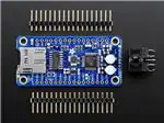


 工商网监
湘ICP备2023018690号
工商网监
湘ICP备2023018690号
