IsoLoop
®
IL711/IL610 MSOP Isolated
Switch-Mode Power Supply
Demonstration Board
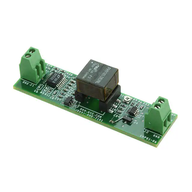
Board No.: SMPS1-01
NVE Corporation
(952) 829-9217
iso-apps@nve.com
www.IsoLoop.com
www.nve.com
�Overview
This board demonstrates an isolated, high-efficiency synchronous buck converter switch-mode
power supply (SMPS) using the world’s smallest isolators, NVE IsoLoop® MSOP Isolators.
The board has three channels of isolation to ensure the output is electrically isolated from the input.
A two-channel MSOP-8 isolator isolates synchronous rectification and a single-channel, failsafe,
MSOP-8 isolator and simple pulse-width modulation circuitry isolates output-voltage feedback.
MSOP isolators minimize board area. Despite the compact components, the transformer,
isolators, and circuit board maintain at least 3 mm creepage. Other IsoLoop versions can be used
with similar circuitry to provide 2.5 kVRMS or 5 kVRMS isolation and as much as 8 mm creepage.
High speed, small size, low EMI, and high reliability make IsoLoop Isolators ideal for switchmode power supplies. A remarkable 44000-year barrier life provides MTBFs thousands of
times better than optocouplers or other solid-state isolators. Key evaluation board and isolator
specifications are summarized as follows:
Evaluation Board Specifications
• Input voltage: 12 V nominal (11 V – 14 V)
• Nominal output voltage: 3.3 ± 0.05 V
• Maximum output current: 750 mA
• Overcurrent protection
• Switching frequency: ~130 kHz
• 1.2 kVRMS isolation / one minute per UL1577
• 85°C operating temperature
• 3 mm creepage spacing
IsoLoop Isolator Features
• 300 ps pulse width distortion for minimal deadtime
• 100 ps pulse jitter for high precision
• 50 kV/µs transient immunity
• No carriers or internal clocks for very low EMI emissions
• 44000 year barrier life
• Package options including:
– Ultraminiature MSOP-8 (2.5 kVRMS isolation; 600 Working Voltage)
– Industry-standard SOIC-8 (2.5 kVRMS isolation; 600 Working Voltage)
– True 8 mm creepage wide-body (5 kVRMS isolation; 1000 Working Voltage)
Visit www.nve.com for IsoLoop® datasheets.
2
�Isolation
Barrier
Board Layout
PWM power
controller
Power
transformer
+3.3V
regulated
output
TOP ASSEMBLY
Output
trim
Output-side
reference
BOTTOM ASSEMBLY
Approx. 2X actual size
Unregulated
input
(+12V nom.)
Voltage feedback
PWM circuitry
Controller
regulator
Output filter
capacitors
Output filter
inductor
Synchronous
rectifier
MOSFETs
Power-control
MOSFETs
IL610-1E
1-channel failsafe
isolator for voltage
feedback
IL711-1E
2-channel isolator
for synchronous rectification
3
�PCB Layers
LAYER 4 (BOTTOM)
LAYER 3
LAYER 2
LAYER 1 (TOP)
Top Views
(approx. 2X actual size)
Contact iso-apps@nve.com for design files.
4
�Bill of Materials
Reference
C5, C23
C6, C8
C3, C9
C24
C1, C4
C13, C14, C15, C19,
C20, C21, C22
C10, C17
C12
C11
D1
R19
R8
R13
R1
R28, R29
R3, R10, R23, R26, R27
R25
R7
R12
R5
R6, R9
R11
R14
L1
Qty
2
2
2
1
2
Part Description
47pF, 16V, 0402
270pF, 16V, 0402
1nF, 16V, 0402
.01µF, 16V, 0402
.068µF, 16V, 0402
Package
0402
0402
0402
0402
0402
7
.1µF, 16V, 0402
0402
2
1
1
1
1
1
1
1
2
5
1
1
1
1
2
1
1
1
2.2µF, 16V, 0402
47µF, 16V, 1210
220µF, 6.3V, 1210
CDSQR400B Switching Diode
0.033Ω, 0603
100Ω, 0402
390Ω, 0402
1.5kΩ, 0402
4.99kΩ, 0402
10kΩ, 0402
20kΩ, 0402
27kΩ, 0402
33kΩ, 0402
Optional (not factory installed)
100kΩ, 0402
300kΩ, 0402
PVA2A223A01R00 22kΩ Trimmer
22µH, 1.5A, 1816
Transformer, 560µH, 8:3,
Pulse Electronics PH9185.083NL
Screw Terminal, 2 position, 0.1"
IRLML6244TRPBF MOSFET
Linear Tech LTC3723 EGN-2#PBF
PWM Controller
NC7S14M5X Invertor
ISL21010DFH312Z-TK 1.25V Ref
IL711-1E 2-channel MSOP Isolator
TI LP2985-10DBVR Regulator
TLV3502AQDCNRQ1 Dual Comp
IL610-1E Passive-Input Isolator
PCB
0402
1210
1210
0402
0603
0402
0402
0402
0402
0402
0402
0402
0402
0402
0402
SMD
0402
1816
T1
1
J1, J2
Q1, Q2, Q3, Q4
2
4
U1
1
U2
U4
U5
U6
U7
U8
SMPS1-06
1
1
1
1
1
1
1
5
SMD
SOT23-3
SSOP-16
SOT23-5
SOT23-3
MSOP-8
SOT23-5
SOT23-8
MSOP-8
�Circuit Description
Circuit Overview
The demonstration circuit has three main sections: power control, synchronous rectification, and
voltage control. The power control section modulates power to the primary of the transformer.
The synchronous rectification section uses synchronously-switched MOSFETs to provide a DC
output from the transformer secondary. Finally, the voltage control section controls the output
by feeding back a pulse-width modulated signal corresponding to the output voltage. The board
has three channels of isolation to provide an electrically isolated output.
Power Control
The PWM Controller (U1) varies the duty cycle of two push-pull power-control MOSFETs
(Q2 and Q3), to regulate to the desired output. The controller oscillator frequency is set by C6,
in this case to around 260 kHz. The switching frequency for the push-pull and synchronous
rectifier MOSFETs is half the controller frequency (roughly 130 kHz). The transformer (T1)
transfers power to the secondary while maintaining isolation. The formulas for approximate
switching frequency are:
f U1.8 ≈
1
(14 kΩ)(C6)
f SWITCH ≈
1
(28 kΩ)(C6)
Powering the controller
At least 10.7 V (VUVLO(MAX)) on VCC is required for Controller start-up. Once the Controller is
running, a minimum 7 V, maximum 10 V supply is needed for operation. In this circuit, a
“trickle charge” through resistor R1 starts the controller. Diode D1 allows VCC to go above the
10 V regulator (U6) output as required for start-up. After the Controller’s start-up cycle, its
power consumption increases, so VCC drops. When VCC drops below approximately 9.3 V, U6
begins supplying Controller power. D1 also drops the regulator output below the 10 V absolute
maximum supply to the Controller from a low-impedance source, even if the regulator is at the
high end of its output specification. The minimum input voltage is a function of the Controller
minimum start-up supply, Controller start-up current, and R1:
VIN(MIN) = VCCUV(MAX) + (I CCST(MAX))(R1); VCCUV(MAX) = 10.7 V; I CCST(MAX) = 250 µA
The 1.5kΩ value for R1 allows a minimum input voltage of 11.1 V. A larger resistor increases
the minimum input voltage; a lower value decreases efficiency by dissipating more power.
This demonstration board has a maximum input voltage maximum input voltage of 16 V,
which is limited by the maximum U6 input.
In some SMPS designs, controller operating power is provided by an auxiliary transformer
winding. This avoids a controller regulator at the expense of a more complicated transformer.
6
�Circuit Description
System turn-on and turn off voltages
The Controller has an input pin for Under-Voltage Lock-Out (UVLO), which is not used on
this board. For precise control of low-input on and off voltages, UVLO can be connected to
the input voltage through a resistor divider. The Controller shuts down gracefully if UVLO is
less than 5V.
Soft start
C1 sets a controlled ramp of the power-switching duty cycle for soft start on power up or after an
overload shutdown. A 0.068 µF capacitor sets the soft-start time (t SS ) at approximately 25 ms:
t SS = (385kΩ)(C1)
The soft start time should be much longer than the voltage feedback cutoff frequency set by
R23, R25, and C24. With active circuitry in the feedback loop, soft start will only be effective
over a limited range near the desired outtput voltage.
MOSFET dead time
R5 can be used to program the “dead time,” which is the minimum time between one of the
Q2 or Q3 power-control MOSFETs turning off and the other turning on. This ensures both
push-pull MOSFETs are not on at the same time at high duty cycles. The resistor is omitted in
this demonstration because it does not normally run at high duty cycles, so the dead time is the
Controller’s default.
Current limiting
R19 sets cycle-by-cycle current limiting, as well as “hiccup mode” short-circuit protection,
where the controller resets and initiates a soft-start cycle. The 0.033Ω value sets cycle-bycycle MOSFET current limits (I C-C ) at approximately 9 A, which provides some margin above
peak operating currents. The controller sets the short-circuit protection (I SCP ) at twice the
cycle-by-cycle limit, or 18 A in this case. The current limit calculations are:
I C-C =
0.3V
R19
I SCP =
0.6V
R19
Synchronous Rectification
The controller turns on synchronous rectification MOSFETs Q1 and Q4 in synchronization
with the power-control MOSFETs. This means the MOSFETs are on when their drain voltages
are positive. This synchronous rectification is more efficient than diode rectification because it
eliminates diodes’ inherent forward voltage losses.
[continued after schematic...]
7
�Isolated Switch-Mode Power Supply Schematic
U7.2
Isolation
Barrier
~1 MHz
U2.4
U1.13
1.2V = 0 ERROR
1
6
J1
12V IN
1
2
2
VIN
3
ON/OFF
1
OUT
IN
BYPASS
GND
4
15
47µ
C17
2.2µ
3
+5V
1
R11
300k
R5
NC
12
9
C8
270p
R3
10k
16
C1 .068µ
14
8
C6 270p
Q2
VCC
UVLO
DVRA
U1 DRVB
LTC3723-2
VREF
CS
DPRG
RAMP
SDRA
SDRB
SPRG
SS
COMP
CT
FB
GND
7
Q4
6
Q3
2
1
C10
2.2µ
3
1
R12 33k
3
R14
22k
Q1 3
2
4
3
2
R19
.033
C9
.001µ
R26
10k
R27
11 R7 27k
13
2
R8 100
10
C4
C3 .068µ
.001µ
10k
R23
10k
1
+5V
C15 1
.1µ
2
3
R28
R29
4.99k 4.99k
4
VDD1
IN1
OUT1
IN2
OUT2
GND1
GND2
IL711-1E
R25
20k
4
U2 5
2
8
C21 7
.1µ
6
5
VDD2
OUT
GND
IL610-1E
+
1
R9
100k
- 2
R10
10k
8
7
C14
C5
.1µ
47p
6
5
Vout
U5
U4
ISL21010 1
+
6
IN
U7
4 1.25V 2
OUT
½
TLV3502 5
GND
3
C19
.1µ
C22
.1µ
C23 47p
VDD
Voe
U7
2
Vout
+5V
C24
.01µ
½
TLV3502
7
1
R6
100k
4
3
NC7S14M5X 3
8
C11
220µ
T1
5
D1
2 U6
LP2985-10
C12
+
R1
1.5k
5
Vout
L1 22µH
5
J2
3.3V OUT
2
-
3
R13 390
+
2
U8
9
8
3
1
�Circuit Description
Synchronous rectification isolation
An IL711V-1E two-channel isolator (U5) isolates the MOSFETs from the controller. The isolator’s
low pulse-width distortion minimizes deadtime and maximizes efficiency. Its speed also
enables higher switching frequencies, which allows smaller inductive elements. High isolator
drive capability allows-high gate-charge MOSFETs.
MOSFET turn-off delay
The delay between power-control synchronous rectifier MOSFET turn-offs can be adjusted from
approximately 20 ns to 200 ns with R3 values of 10 kΩ to 200 kΩ. The delay can optimize
efficiency by compensating for MOSFET speeds and inductive phase shifts. This demonstration
uses just a 20 ns delay because it has fast MOSFETs and a relatively small transformer.
Voltage Control
The output supply voltage is determined by three voltage references and several resistors. The
references are 1.2 V and 5 V controller references (VFB and VREF), and a separate 1.25 V outputside reference (VU4). The critical voltage dividers are R6, R9, and R12, which scales the
sawtooth waveform; and R23/R25, which scales the isolated voltage feedback signal.
Half of U7 forms a relaxation oscillator with a sawtooth waveform amplitude proportional to
the supply voltage. It is also the pulse-width modulation time base. R6 and R9 are equal to
center the waveform. The peak-to-peak sawtooth amplitude is set by R12 (a trimmer in series
with R12 on this board can be used to adjust the output voltage):
VU7.2(P-P) = VOUT [1 – R12/(R9/2 + R12)]; R6 = R9
The other half of U7 compares the sawtooth to the reference to create a pulse-width modulated
signal that follows the output voltage. The sawtooth amplitude and the reference voltage
determine the feedback control range. The minimum control voltage (where the feedback duty
cycle is zero) and maximum control range (100% duty cycle), are calculated as follows:
VOUT(MIN) = VU4 (R9 + 2R12)/(R9 + R12); VU4 = 2.5 V; R6 = R9
VOUT(MAX) = VU4 (2 + R9/R12); VU4 = 2.5 V; R6 = R9
This oscillator circuit has a wide control range. For this demonstration, the minimum control
range was set at approximately 2.8 V, and the maximum is nearly 9 V, which is well beyond
the range of interest. The voltage-feedback pulse-width modulation frequency is approximately
1 MHz, calculated as follows:
f U7.6 =
1
; R6 = R9
2(R10)(C5)[ln(1+R9/R12)]
10
�Circuit Description
The exact frequency is not critical because the output voltage is encoded as duty cycle. The U7
output duty cycle varies with the output voltage according to the following relationship:
δU7.6 = 0.5 +
ln (VOUT / VU4 – 1)
; VU4 = 1.25 V; R6 = R9
2 ln (1 + R9/R12)
The following graph shows that relationship:
Feedback Duty Cycle
100%
80%
60%
40%
20%
0%
2
2.5
3
3.3V
3.5
4
Output Voltage
4.5
5
5.5
As shown in the figure above, The duty cycle is 50% when the output voltage is twice the
output-side reference voltage, or 2.5 V. The components in this board set the duty cycle at
approximately 70% at the 3.3 V output target. Because it is part of a closed-loop system, dutycycle nonlinearity does not degrade accuracy, and the circuit is simpler than high-linearity
pulse-width modulators.
Feedback isolation
The pulse-width modulated feedback signal is isolated by an IL610-1E single-channel MSOP
isolator (U8), which is smaller and longer life than analog optocouplers commonly used for
this purpose. Unlike most digital isolators, the IL610 is inherently failsafe, and guarantees a
high output when there is no coil current. The output of Invertor U2 will then be low with no
coil current, so the controller will call for power.
The (-) isolator coil terminal is used as the input, so that the isolator is configured as an
invertor. The inverted configuration ensures the U2 output phase is the same as the output of
comparator U7. The isolator coil resistor (R13) is selected to provide at least the 5 mA
minimum DC Input Threshold at the minimum operating voltage of 2.8 V for the output
circuitry. C3 is a “boost capacitor” that ensures the isolator turns on under marginal conditions.
11
�Circuit Description
R23, R25, and C24 scale and filter the isolated PWM signal to convert it back to an isolated
feedback voltage for the controller. A more sophisticated filter or faster feedback components
can be used for applications requiring faster transient response. The Controller’s 5 V reference
powers the invertor, so the feedback voltage is proportional to the 5 volt reference and the duty
cycle, scaled by the R23 and R25 voltage divider:
VU1.13 = δU7.1 (VREF)(R23)/(R23 + R25); VREF = 5V
Setting the output voltage
A voltage-mode PWM Controller version is used for U1 because it is compatible with pulsewidth modulation of the feedback voltage. The Controller compares the feedback voltage to an
internal 1.2 V reference (VFB). Since the average feedback voltage should be 1.2 V at the
desired 3.3 V output:
δ VOUT = VFB / VREF; VFB = 1.2V; VREF = 5V
The feedback duty cycle at the desired 3.3 V is approximately 70% in this case, calculated
from the previous equation for δU7.1. R23 and R25 can then be used to set the output voltage:
R25/R23 = δ VOUT (VREF/VFB) – 1; VREF = 5V; VFB = 1.2V
A trim resistor on the output side can adjust the output for demonstration purposes. Optional
R23 can be used to form a voltage divider for another means of adjustment.
Filtering and Frequency Compensation
Output filter
The output capacitor filters out ripple. In this design there are two primary ripple sources, the
synchronous rectification and the PWM voltage feedback. Synchronous rectification ripple is
inversely proportional to twice the switching frequency (because full-wave rectification is
used). Ignoring the ripple reducing effects of L1, the synchronous rectification output ripple
component is estimated as follows:
VRIPPLE-SWITCH = I LOAD / [(C11)(2f SWITCH)]
A 220 µF capacitor (C11) with the 130 kHz switching frequency provides ripple of less than
10 mV at a 500 mA load. A parallel low-ESR capacitor (C10) minimizes ripple from inductive
current changes.
PWM signal filter
R25 and C24 filter the isolated PWM signal and help ensure system closed-loop stability. The
filter reduces PWM-induced ripple and error amplifier noise. However, the time constant also
limits transient response time.
12
�Circuit Description
The filter cutoff frequency is well above the output filter and controller compensation cutoff
frequencies so the closed-loop control is fast enough for stability. For the simple single-pole
filter, the ripple in the PWM signal is approximately:
VRIPPLE-U1.13 = VFB /(τU1.13 fU7.1); VFB = 1.2 V;
τU1.13 = (C24)[(R25)(R23)/(R25+R23)]
PWM ripple will be reflected to the output but reduced by the output filter capacitor:
VRIPPLE-PWM = (VRIPPLE-U1.13)(I LOAD)/[(VFB)(fU7.6)(C11)]; VFB = 1.2 V
A more sophisticated filter or higher frequency feedback can be used for faster transient response.
Error amplifier gain
The controller error amplifier gain at AC frequencies well above the amplifier compensation
cutoff frequency is:
AERROR-AC = R7 / R25
Higher gain provides less steady-state error at the expense of gain margin and therefore stability.
Controller compensation
(R7)(C4) improves accuracy and stability by increasing the DC gain. Filters created by
(R23||R25)(C24) and (R7)(C3) limit high-frequency gain to reduce ripple and improve noise
immunity.
Level shifting
System components run on three different supplies: the 9.3 V nominal controller supply, the
5 V controller reference supply, and the 3.3 V supply output. The controller’s synchronous
rectifier driver voltage can go as high as the controller supply, but the U5 isolator is powered
from the 5 V primary-side reference supply. Therefore voltage dividers keep the isolator inputs
below 5 V but above their 2.4 V minimum Logic High Input Voltage.
The synchronous rectifier MOSFETs are driven by the 3.3 V side of U5, so the MOSFETs are
selected for a gate-source threshold voltage of well below 3.3 V. The isolator also provides
inherent level shifting between the 3.3 V feedback signal and the 5 V reference supply.
Maintaining Creepage
Creepage distances are often critical in power supplies circuits. In addition to meeting JEDEC
standards, NVE isolator packages have unique creepage specifications. Recommended pad
layouts are included in the isolator datasheets. Standard pad libraries, especially MSOPs,
sometimes extend under the package, compromising creepage and clearance. Ground and
power planes are also spaced to avoid compromising clearance.
13
�One- and Two-Channel IL700-Series Isolators
Award-winning IsoLoop® IL700-Series
Isolators are ideal for switch-mode power
supplies because of their high speed, small
size, low EMI, and high reliability. Twochannel isolators are popular choices for
SMPS.
IN1
OUT1
IN2
OUT2
IL711
All IsoLoop Isolators have a unique polymerceramic composite isolation barrier for a
remarkable 44000-year barrier life.
IN1
OUT1
OUT2
Various grades, channel configurations and
packages are available.
IN2
IL712
OUT1
VOE
IN1
IN2
OUT1
OUT2
IL721
IL710
IsoLoop
Model
IL710V-1E
IL711V-1E
IL712V-1E
IL710T-3E
IL711T-3E
IL712T-3E
IL721T-3E
IL711VE
IL721VE
IN1
Transmit/
Receive
Channels
1/0
2/0
1/1
1/0
2/0
1/1
1/1
2/0
1/1
Isolation
(per UL1577)
2500 VRMS
2500 VRMS
2500 VRMS
2500 VRMS
2500 VRMS
2500 VRMS
2500 VRMS
5000 VRMS
5000 VRMS
Max.
Temp.
100 C
100 C
100 C
125 C
125 C
125 C
125 C
125 C
125 C
Key Features
Ultraminiature
Ultraminiature
Ultraminiature
High Temperature
High Temperature
High Temperature
High Temperature
True 8 mm Creepage
True 8 mm Creepage
Visit www.nve.com for datasheets.
14
Package
MSOP8
MSOP8
MSOP8
SOIC8
SOIC8
SOIC8
SOIC8
0.3" SOIC16
0.3" SOIC16
�One- and Two-Channel IL600 Failsafe Isolators
Unique IL600-Series Isolators are inherently
failsafe with passive inputs similar to LEDinput optocouplers. Inputs can be configured
for inverting or non-inverting. Parts are
available in SOIC and unique MSOP packages,
as well as bare die for chip-on-board assembly.
Unlike optocouplers, all IsoLoop Isolators
have a unique polymer-ceramic composite
isolation barrier for a remarkable 44000-year
barrier life.
VOE
OUT1
IN1
IL610
IN1
OUT1
IN2
OUT2
IL611
VDD1
OUT1
IN1
VDD2
OUT2
IN2
IL612
IsoLoop
Model
IL610-1E
IL611-1E
IL612-1E
IL610-3E
IL611-3E
IL612-3E
Transmit/
Receive
Channels
1/0
2/0
1/1
1/0
2/0
1/1
Isolation
(per UL1577)
1200 VRMS
1200 VRMS
1200 VRMS
2500 VRMS
2500 VRMS
2500 VRMS
Max.
Temp.
85 C
85 C
85 C
85 C
85 C
85 C
Key Features
Failsafe; Ultraminiature
Failsafe; Ultraminiature
Failsafe; Ultraminiature
Failsafe
Failsafe
Failsafe
Visit www.nve.com for datasheets.
15
Package
MSOP8
MSOP8
MSOP8
SOIC8
SOIC8
SOIC8
�Limited Warranty and Liability
Information in this document is believed to be accurate and reliable. However, NVE does not give any
representations or warranties, expressed or implied, as to the accuracy or completeness of such information
and shall have no liability for the consequences of use of such information. In no event shall NVE be liable for
any indirect, incidental, punitive, special or consequential damages (including, without limitation, lost profits,
lost savings, business interruption, costs related to the removal or replacement of any products or rework
charges) whether or not such damages are based on tort (including negligence), warranty, breach of contract or
any other legal theory.
Right to Make Changes
NVE reserves the right to make changes to information published in this document including, without
limitation, specifications and product descriptions at any time and without notice.
Use in Life-Critical or Safety-Critical Applications
Unless NVE and a customer explicitly agree otherwise in writing, NVE products are not designed, authorized
or warranted to be suitable for use in life support, life-critical or safety-critical devices or equipment. NVE
accepts no liability for inclusion or use of NVE products in such applications and such inclusion or use is at
the customer’s own risk. Should the customer use NVE products for such application whether authorized by
NVE or not, the customer shall indemnify and hold NVE harmless against all claims and damages.
Applications
Applications described in this document are illustrative only. NVE makes no representation or warranty that
such applications will be suitable for the specified use without further testing or modification. Customers are
responsible for the design and operation of their applications and products using NVE products, and NVE
accepts no liability for any assistance with applications or customer product design. It is customer’s sole
responsibility to determine whether the NVE product is suitable and fit for the customer’s applications and
products planned, as well as for the planned application and use of customer’s third party customers.
Customers should provide appropriate design and operating safeguards to minimize the risks associated with
their applications and products. NVE does not accept any liability related to any default, damage, costs or
problem which is based on any weakness or default in the customer’s applications or products, or the
application or use by customer’s third party customers. The customer is responsible for all necessary testing
for the customer’s applications and products using NVE products in order to avoid a default of the
applications and the products or of the application or use by customer’s third party customers. NVE accepts no
liability in this respect.
An ISO 9001 Certified Company
NVE Corporation
11409 Valley View Road
Eden Prairie, MN 55344-3617
©NVE Corporation
All rights are reserved. Reproduction in whole or in part is prohibited without the prior written consent of the
copyright owner.
Manual No.: ISB-CB-014
April 2015
NVE Corporation
(952) 829-9217
iso-apps@nve.com
www.IsoLoop.com
www.nve.com
�


 工商网监
湘ICP备2023018690号
工商网监
湘ICP备2023018690号
