Additional Resources:
Product Page
|
3D Model
|
PCB Footprint
date
11/01/2012
page
1 of 6
SERIES: VLD25-SMT │ DESCRIPTION: LED DRIVER
FEATURES
•
•
•
•
•
•
•
•
power LED driver
wide input and output voltage range
SMT package
constant current output
PWM dimming and analogue dimming
short circuit protection
analog dimming
high efficiency up to 96%
RoHS
input
voltage
output
voltage
output
current
ripple and
noise
range
(Vdc)
range
(Vdc)
range
(mA)
max
(mVp-p)
VLD25-300-SMT
5.5 ~ 48
3.3 ~ 36
0 ~ 300
120
PWM+analog
96
VLD25-350-SMT
5.5 ~ 48
3.3 ~ 36
0 ~ 350
120
PWM+analog
96
VLD25-500-SMT
5.5 ~ 48
3.3 ~ 36
0 ~ 500
120
PWM+analog
96
VLD25-600-SMT
5.5 ~ 48
3.3 ~ 36
0 ~ 600
120
PWM+analog
96
VLD25-700-SMT
5.5 ~ 48
3.3 ~ 36
0 ~ 700
120
PWM+analog
96
MODEL
dimming
control
typ
(%)
PART NUMBER KEY
VLD25 - XXX -SMT - X
Base Number
Output Voltage
Packaging Style
cui.com
efficiency
Package Options
"blank" = standard
TR = Tape & Reel
�Additional Resources:
Product Page
|
3D Model
|
PCB Footprint
CUI Inc │ SERIES: VLD25-SMT │ DESCRIPTION: LED DRIVER
date 11/01/2012 │ page 2 of 6
INPUT
parameter
conditions/description
min
operating input voltage
absolute max before device failure
operating input range
5
5.5
quiescent input
current in off mode
Vin = 24 V, Vr < 0.6 V
filter
capacitor
remote on/off
dc-dc ON (Vr on pin 7)
dc-dc OFF
remote pin current
Vr = 5V
typ
max
units
24
55
48
Vdc
Vdc
400
μA
1
μF
open or 2.8 V < Vr < 6V
Vr < 0.6 V
PWM frequency
input voltage - analog dimming
Vin = 5.5 ~ 4.8 V
control voltage analog dimming
full on
full off
driving current analog dimming
Vr = 5 V
0
0.15
4.3
0.20
4.5
1
mA
0.2
kHz
15
V
0.25
4.7
V
V
0.6
A
max
units
36
Vdc
OUTPUT
parameter
conditions/description
min
voltage range
Vin = 48 V , Vo = 3.3 V ~ 36 V
3.3
voltage drop
Vin = 5.5 ~ 48 V, 1 ~ 10 LED
2
current accuracy
output current range analog dimming
typ
±2
Vin = 5.5 ~ 48 V, 1 ~ 10 LED
current stability
Vin = 48 V, Vo = 3.3 V ~ 36 V
temperature coefficient
-40 ~ 71°C ambient
0
4
Vdc
±3
%
100
%
±1
%
±0.015
%/°C
1,000
μF
typ
max
units
typ
max
units
85
71
°C
°C
capacitive load
PROTECTIONS
parameter
conditions/description
short circuit protection
continuous automatic recovery
min
SAFETY AND COMPLIANCE
parameter
conditions/description
EMI/EMC
EN 55015 power port, EN 55015, IEC/EN 61000-4-(2, 3, 4, 5, 6)
RoHS compliant
yes
ENVIRONMENTAL
parameter
conditions/description
min
operating temperature
300/350 mA
500/600/700 mA
-40
-40
storage temperature
-55
maximum case temperature
125
°C
100
°C
max
units
MECHANICAL
parameter
conditions/description
dimensions
0.94 x 0.71 x 0.31 inch (23.86 x 18.1 x 8.0 mm)
min
case material
epoxy resin (UL94-V0)
weight
typ
6
cui.com
g
�Additional Resources:
Product Page
|
3D Model
|
PCB Footprint
CUI Inc │ SERIES: VLD25-SMT │ DESCRIPTION: LED DRIVER
date 11/01/2012 │ page 3 of 6
MECHANICAL DRAWING
unit: mm(inch)
Pin tolerances: ±0.10mm(±0.039inch)
General tolerances: ±0.25mm(±0.010inch)
15.24 0.600
0.50 0.020
(6 PLCS)
1.02 0.040
(6 PLCS)
16
10 9
18.10 0.713
1
7
3.04 0.120
8
2.54 0.100
1.40 0.055
0.20
13.70 0.539
23.86 0.939
0.25 0.010
5° max
7.50 0.295
8.00 0.315
A
RECOMMENDED FOOTPRINT (TOP VIEW)
PIN CONNECTIONS
Function
1
GND
7
ON/OFF/PWM
8
-Vout
9
+Vout
10
analog dimming
16
Vin
17.20 [0.677]
Pin
DETAIL A
SCALE 8 : 1
16
1
10 9
7 8
1.00 [0.039]
2.54 [0.100]
grid: 2.54 x 2.54 mm
cui.com
2.10 [0.100]
�Additional Resources:
Product Page
|
3D Model
|
PCB Footprint
CUI Inc │ SERIES: VLD25-SMT │ DESCRIPTION: LED DRIVER
date 11/01/2012 │ page 4 of 6
APPLICATION NOTES
1.
Digital Dimming Control
50% Duty Cycle
20% Duty Cycle
80% Duty Cycle
Output current(LED appears dimmer)
Output current(LED appears brighter)
Output current
For the rated frequency PWM dimming, the output current of driver matters to the pulse width of the PWM signal, and the numerate please refer to the
following formula:
Io,set refers to the expected output current value.
(DT-0.6)
Io,norm refers to the rated output current
Io,set =
Io,nom
D refers to the pulse width of the PWM signal
T
T refers to the cycle of the PWM signal
Note: The formula only supplies as a reference, and the output current may be a little deviation with different load. The Ton(min) of PWM signal must be
greater than 0.7ms, or the driver can’t be operated normally. It is natural for the driver to generate an audibly noise in dimming process, because the
frequency of the control circuit is within human audibly range (20Hz~20kHz). In order to avoid the human eye can observe the LED flashes, the PWM
dimming frequency is recommended to set above 100Hz.
Analog Dimming Control and Application Example
16
+Vin
1
GND
����
9
VLD25-SMT
8
1st LED
5K1
0-10V
On/Off
(Optional)
10
5K6
Analog Input Voltage
Ouput Current
2.
7
Last LED
��
���9
�9
�9
�9
�9
�9
Voltage Control (0-15 V max.)
cui.com
��9
�Additional Resources:
Product Page
|
3D Model
|
PCB Footprint
CUI Inc │ SERIES: VLD25-SMT │ DESCRIPTION: LED DRIVER
3.
date 11/01/2012 │ page 5 of 6
EMC Recommended Circuit
(Analog Dim)
EMI/RFI conducted EN55022 recommended circuit
1.25mH
+
SMCG51
9 +Vout
VLD25-SMT
1.0uF
2.2uF
470uF
10
16
+Vin
1.0uF
Vout
GND
8-
1
1st LED
7
Last LED
(P W M D im/O N /O FF)
EMI/EMC recommended circuit
LCM
㻗
Vin
V IN
C0
C1
C2
DIM㻖
R1
DI M
C3
G ND
GND
Load
VO-
1. DIM pin is the module's PWM dimming pin
2. While adding circuit, it may extend the PWM dimming output reaction time
EMI/EMC STANDARD
ITEM
STANDARD
LEVEL
PREDICATE
REMARK
EMI conducted
EN 55015
power port
qualification
add external circuit 1
ESD
IEC 61000-4-2:2001
level 2
B
+4kV add external circuit 2
Surge
IEC 61000-4-5:2004
level 2
B
+1kV add external circuit 1
EFT
IEC 61000-4-4:2004
level 2
B
+1kV add external circuit 1
RECOMMENDED PARAMETERS
COMPONENTS
SPECIFICATIONS
Tvs
SMCJ48A, 1500 W (Bringtking)
LCM
6.8 μh CD43 (CEAIYA)
C0
470 μF / 50 V (CapXon)
C1
4.7 μF / 50 V 1210 (TORCH)
C2
2.2 μF / 50 V 1210 (TORCH)
C3
470 PF / 100 V 0805 (TORCH)
R1
680 Ω 0805 (can be replaced by
inductance or magnetic bead)
Recommended Reflow Soldering Profile
250
P ea k .Te mp 24 0 C
1 0 Se c M ax
220 C
200
Temperature ( C)
4.
-Vout
2
1
Notes:
+Vout
VO+
VLD25-SMT
Tvs
60 Sec Max
(> 220 C )
150
100
50
0
Time (sec.)
cui.com
�Additional Resources:
Product Page
|
3D Model
|
PCB Footprint
CUI Inc │ SERIES: VLD25-SMT │ DESCRIPTION: LED DRIVER
date 11/01/2012 │ page 6 of 6
REVISION HISTORY
rev.
description
date
1.0
initial release
02/20/2012
1.01
V-Infinity branding removed
09/07/2012
1.02
added TR package option
11/01/2012
The revision history provided is for informational purposes only and is believed to be accurate.
Headquarters
20050 SW 112th Ave.
Tualatin, OR 97062
800.275.4899
Fax 503.612.2383
cui.com
techsupport@cui.com
CUI offers a two (2) year limited warranty. Complete warranty information is listed on our website.
CUI reserves the right to make changes to the product at any time without notice. Information provided by CUI is believed to be accurate and reliable. However, no responsibility is
assumed by CUI for its use, nor for any infringements of patents or other rights of third parties which may result from its use.
CUI products are not authorized or warranted for use as critical components in equipment that requires an extremely high level of reliability. A critical
component is any component of a life support device or system whose failure to perform can be reasonably expected to cause the failure of the life support device or system, or to
affect its safety or effectiveness.
�
很抱歉,暂时无法提供与“VLD25-600-SMT-TR”相匹配的价格&库存,您可以联系我们找货
免费人工找货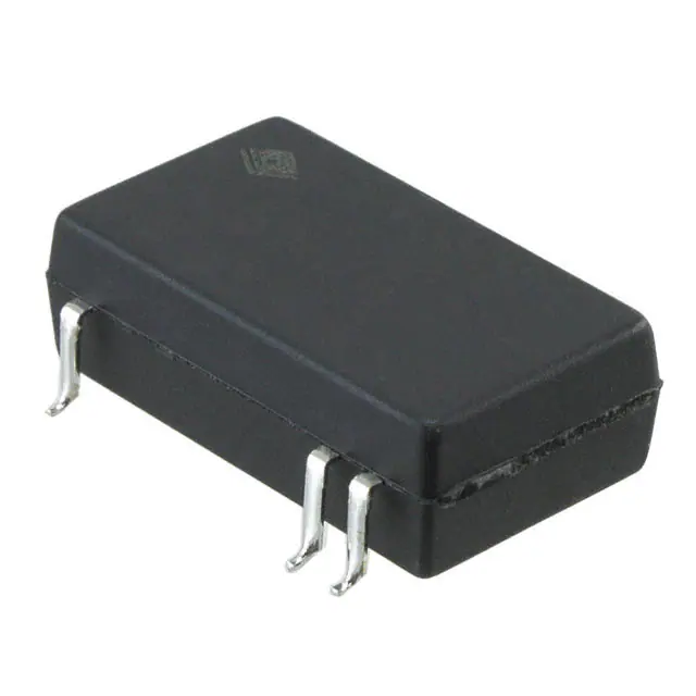


 工商网监
湘ICP备2023018690号
工商网监
湘ICP备2023018690号
