SHEN ZHEN XIN FEI HONG ELECTRONICS CO.,LTD
FH3400C
N-Channel Enhancement Mode MOSFET
Description
General Features
The FH3400C uses advanced trench technology to
provide excellent RDS(ON), low gate charge and high
density cell Design for ultra low on resistance. This
device is suitable for use as a load switch or in PWM
applications.
-
Application
PWM applications
Load switch
Schematic diagram
VDS =30V,ID =4.7A
RDS(ON) (Typ.)=27mΩ
RDS(ON) (Typ.)=30mΩ
RDS(ON) (Typ.)=39mΩ
@V GS = 10V
@VGS = 4.5V
@VGS = 2.5V
High power and current handing capability
Lead free product is acquired
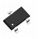
Surface mount package
SOT-23 top view
Marking and Pin Assignment
Absolute Maximum Ratings (TA=25 ℃ unless otherwise noted)
symbol
limit
unit
Drain-source voltage
VDS
30
V
Gate -source voltage
V GS
±12
V
Drain current-continuousa@Tj=125℃
-pulse db
ID
4.7
A
IDM
19
A
Drain-source Diode forward current
Is
2
A
Maximum power dissipation
PD
1.4
W
Operating junction Temperature range
Tj
-55 — 150
℃
parameter
Thermal Characteristics
Thermal Resistance junction-to ambient
www.xfhong.com
Rth JA
109
1/6
℃/W
Ver1.0
�FH3400C
N-Channel Enhancement Mode MOSFET
Electrical Characteristics (TA=25℃ unless otherwise noted)
Parameter
Symbol
Condition
Min
Typ
Max
Unit
OFF Characteristics
Drain-source breakdown voltage
BVDSS
VGS=0V, ID=250µA
30
-
-
V
Zero gate voltage drain current
IDSS
VDS=30V, VGS=0V
-
-
1
µA
Gate-body leakage
IGSS
VDS=0V, VGS=±12V
-
-
±100
nA
VGS(th)
VDS=VGS, ID=250µA
0.6
0.9
1.5
V
VGS= 10V, ID=4A
-
27
35
VGS=4.5V, ID =4A
-
30
36
39
52
-
35
-
-
490
-
-
66
-
-
42
-
-
3
-
-
2.5
-
-
25
-
-
4
-
-
6
-
-
1.3
-
-
1.8
-
-
0.76
1.16
ON Characteristics
Gate threshold voltage
Drain-source on-state resistance
RDS(ON)
VGS=2.5V, ID=2A
Forward transconductance
gfs
VGS=5V, ID =4.7A
mΩ
S
Dynamic Characteristics
Input capacitance
CISS
Output capacitance
COSS
Reverse transfer capacitance
CRSS
VDS=15V ,VGS=0V
f=1.0MHz
pF
Switching Characteristics
Turn-on delay time
Rise time
Turn-off delay time
Fall time
Total gate charge
tD(ON)
tr
tD(OFF)
tf
VDS=15V
VGS=10V
RL=2.6 ohm
R GEN=3ohm
Qg
Gate-source charge
Qgs
Gate-drain charge
Qgd
VDS=15V,ID =4.7
AVGS=4.5V
ns
nC
DRAIN-SOURCE DIODE CHARACTERISTICS
Diode forward voltage
VSD
VGS=0V,Is=1A
V
Notes:
a. surface mounted on FR4 board,t≤10sec
b. pulse test: pulse width≤300μs,duty≤2%
c. guaranteed by design, not subject to production testing
www.xfhong.com
2/6
Ver1.0
�FH3400C
N-Channel Enhancement Mode MOSFET
Typical Performance Characteristics
www.xfhong.com
3/6
Ver1.0
�FH3400C
www.xfhong.com
N-Channel Enhancement Mode MOSFET
4/6
Ver1.0
�FH3400C
www.xfhong.com
N-Channel Enhancement Mode MOSFET
5/6
Ver1.0
�FH3400C
N-Channel Enhancement Mode MOSFET
Package Information : SOT-23
Symbol
A
A1
A2
b
c
D
E
E1
e
e1
L
L1
θ
www.xfhong.com
Dimensions In Millimeters
Min.
Max.
0.900
0.000
0.900
0.300
0.080
2.800
1.200
2.250
1.150
0.100
1.050
0.500
0.150
3.000
1.400
2.550
Dimensions In Inches
Min.
Max.
0.035
0.000
0.035
0.012
0.003
0.110
0.047
0.089
0.950 TYP.
1.800
0.037 TYP.
2.000
0.071
0.550 REF.
0.300
0°
0.045
0.004
0.041
0.020
0.006
0.118
0.055
0.100
0.079
0.022 REF.
0.500
8°
6/6
0.012
0°
0.020
8°
Ver1.0
�
很抱歉,暂时无法提供与“FH3400C”相匹配的价格&库存,您可以联系我们找货
免费人工找货- 国内价格
- 1+0.36061
- 100+0.33657
- 300+0.31253
- 500+0.28849
- 2000+0.27647
- 5000+0.26926


 工商网监
湘ICP备2023018690号
工商网监
湘ICP备2023018690号
