HGB027N10A
HGP027N10A
,
P-1
HGK027N10A
100V N-Ch Power MOSFET
Feature
◇ High Speed Power Switching
◇ Enhanced Body diode dv/dt capability
◇ Enhanced Avalanche Ruggedness
◇ 100% UIS Tested, 100% Rg Tested
◇ Lead Free, Halogen Free
VDS
RDS(on),typ TO-263
RDS(on),typ TO-247
RDS(on),typ TO-220
ID (Sillicon Limited)
Application
◇ Synchronous Rectification in SMPS
◇ Hard Switching and High Speed Circuit
TO-263
◇ DC/DC in Telecoms and Inductrial
VGS=10V
VGS=10V
VGS=10V
V
mW
mW
mW
A
100
2.2
2.4
2.5
248
Drain
Pin2
TO-220
Gate
Pin 1
Part Number
HGB027N10A
HGK027N10A
HGP027N10A
Package
Marking
TO-263 GB027N10A
TO-247 GK027N10A
TO-220 GP027N10A
TO-247
Absolute Maximum Ratings at T j=25℃ (unless otherwise specified)
Parameter
Continuous Drain Current (Silicon Limited)
Src
Pin3
Symbol
ID
Continuous Drain Current (Package Limited)
Drain to Source Voltage
VDS
Gate to Source Voltage
VGS
Pulsed Drain Current
IDM
Avalanche Energy, Single Pulse
EAS
Power Dissipation
PD
Operating and Storage Temperature
TJ, Tstg
Conditions
TC=25℃
TC=100℃
TC=25℃
L=0.4mH, TC=25℃
TC=25℃
-
Value
248
176
180
100
Unit
A
±20
800
720
341
-55 to175
V
V
A
mJ
W
℃
Max
60
0.44
Unit
℃/W
℃/W
Absolute Maximum Ratings
Parameter
Thermal Resistance Junction-Ambient
Thermal Resistance Junction-Case
Ver 1.0
Symbol
RqJA
RqJC
Apr. 2020
�HGB027N10A
HGP027N10A
,
P-2
HGK027N10A
Electrical Characteristics at T j=25℃ (unless otherwise specified)
Static Characteristics
Parameter
Symbol
Conditions
Value
min
typ
max
Unit
Drain to Source Breakdown Voltage V(BR)DSS
VGS=0V, ID=250mA
100
-
-
Gate Threshold Voltage
VGS(th)
VGS=VDS, ID=250mA
2.0
3.0
4.0
Zero Gate Voltage Drain Current
IDSS
VGS=0V, VDS=100V, Tj=25℃
-
-
1
VGS=0V, VDS=100V, Tj=100℃
-
-
100
Gate to Source Leakage Current
IGSS
VGS=±20V, VDS=0V
Drain to Source on Resistance
Drain to Source on Resistance
±100 nA
2.7 mW
2.9 mW
V
mA
-
-
RDS(on)
VGS=10V, ID=20A
TO-263
-
2.2
RDS(on)
VGS=10V, ID=20A
TO-247
-
2.4
Drain to Source on Resistance
RDS(on)
VGS=10V, ID=20A
TO-220
-
2.5
3
Transconductance
gfs
VDS=5V, ID=20A
-
75
-
mW
S
Gate Resistance
RG
VGS=0V, VDS Open, f=1MHz
-
1.5
-
W
-
7684
-
-
114
-
-
21
-
-
106
-
-
24
-
22
-
Dynamic Characteristics
Input Capacitance
Ciss
Output Capacitance
Coss
Reverse Transfer Capacitance
Crss
Total Gate Charge
Qg(10V)
Gate to Source Charge
Qgs
VGS=0V, VDS=50V, f=1MHz
VDD=50V, ID=20A, VGS=10V
pF
nC
Gate to Drain (Miller) Charge
Qgd
-
Turn on Delay Time
td(on)
-
28
-
Rise time
tr
-
22
-
Turn off Delay Time
td(off)
-
52
-
Fall Time
tf
-
13
-
-
0.9
1.2
V
-
65
-
ns
-
455
-
nC
VDD=50V, ID=20A, VGS=10V,
RG=10W,
ns
Reverse Diode Characteristics
Diode Forward Voltage
VSD
Reverse Recovery Time
trr
Reverse Recovery Charge
Qrr
Ver 1.0
VGS=0V, IF=20A
VR=50V, IF=20A, dIF/dt=500A/ms
Apr. 2020
�HGB027N10A
HGP027N10A
,
Fig 1. Typical Output Characteristics
P-3
HGK027N10A
Figure 2. On-Resistance vs. Gate-Source Voltage
8
120
10V
5V
ID=20A
100
4.5V
6
80
RDS(ON) (mW)
125°C
ID (A)
60
40
4
2
25°C
Vgs=4V
20
0
0
0
1
2
2
3
4
6
8
10
VGS (V)
VDS (V)
Figure 3. On-Resistance vs. Drain Current and Gate Voltage
Figure 4. Normalized On-Resistance vs. Junction Temperature
5
2.2
ID=20A
2
Normalized On-Resistance
4
VGS=6V
RDS(ON) (mW)
3
VGS=10V
2
1
VGS=10V
1.8
1.6
1.4
VGS=6V
1.2
1
0
0.8
0
5
10
15
20
0
25
50
ID (A)
75
100
125
150
175
Temperature (°C)
Figure 5. Typical Transfer Characteristics
Figure 6. Typical Source-Drain Diode Forward Voltage
20
1.E+02
VDS=5V
1.E+01
15
125°C
1.E+00
125℃
ID(A)
25℃
IS (A)
10
25°C
1.E-01
5
1.E-02
0
1.E-03
2
3
4
VGS(V)
Ver 1.0
5
0.2
0.4
0.6
0.8
1.0
VSD (V)
Apr. 2020
�HGB027N10A
HGP027N10A
,
Figure 7. Typical Gate-Charge vs. Gate-to-Source Voltage
P-4
HGK027N10A
Figure 8. Typical Capacitance vs. Drain-to-Source Voltage
10000
10
VDS=50V
ID=20A
Ciss
8
Capacitance (pF)
1000
VGS (V)
6
4
Coss
100
Crss
10
2
0
1
0
25
50
75
100
125
0
20
40
80
100
VDS (V)
Qg (nC)
Figure 9. Maximum Safe Operating Area
Figure 10. Maximun Drain Current vs. Case Temperature
1000.0
300
RDS(ON) limited
10ms
100.0
Current rating ID(A)
100ms
1ms
10.0
10ms
ID (Amps)
60
DC
10s
TJ(Max)=175°C
TC=25°C
1.0
0.1
Silicon Limited
200
Package Limited
100
0
0.0
0.01
0.1
1
10
100
1000
0
25
VDS (V)
50
75
100
125
150
175
TAmbient(℃)
Figure 11. Normalized Maximum Transient Thermal Impedance, Junction-to-Ambient
Duty=Ton/T
Peak TJ=TC+PDM.ZqJC.RqJC
RqJC=0.44℃/W
1
Duty=0.5
ZqJA Normalized Transient
Thermal Resistance
0.3
0.1
0.05
0.1
0.01
0.03
0.01
single pulse
0.001
1E-05
0.0001
0.001
0.01
0.1
1
Pulse Width (s)
Ver 1.0
Apr. 2020
�HGB027N10A
HGP027N10A
,
HGK027N10A
P-5
Inductive switching Test
Gate Charge Test
Uclamped Inductive Switching (UIS) Test
Diode Recovery Test
Ver 1.0
Apr. 2020
�HGB027N10A
HGP027N10A
,
HGK027N10A
P-6
Package Outline
TO-220, 3 leads
Ver 1.0
Apr. 2020
�HGB027N10A
HGP027N10A
,
HGK027N10A
P-6
Package Outline
TO-263, 3 leads
Ver 1.0
Apr. 2020
�HGB027N10A
HGP027N10A
,
HGK027N10A
P-6
Package Outline
TO-247, 3 leads
Ver 1.0
Apr. 2020
�
很抱歉,暂时无法提供与“HGB027N10A”相匹配的价格&库存,您可以联系我们找货
免费人工找货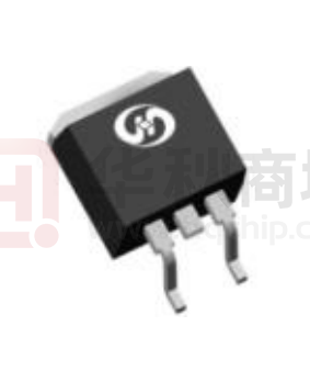


 工商网监
湘ICP备2023018690号
工商网监
湘ICP备2023018690号
