Nuvoton
SMBus GPIO Controller
W83L603G
W83L604G
Revision: 1.1
Date: July, 2008
�W83L603G/W83L604G
W83L603G/W83L604G
Datasheet Revision History
1
PAGES
DATES
VERSION
WEB VERSION
N.A.
Aug./06
1.0
1.0
July/08
1.1
MAIN CONTENTS
Initial Version for customer
Change logo
- I -
Publication Release Date: July, 2008
Revision 1.1
�W83L603G/W83L604G
Table of Contents1.
GENERAL DESCRIPTION ......................................................................................................... 1
2.
FEATURES ................................................................................................................................. 1
2.1
General Features .....................................................................................................................1
2.2
Key Specifications ....................................................................................................................1
3.
PIN CONFIGURATION ............................................................................................................... 2
4.
PIN DESCRIPTION..................................................................................................................... 3
4.1
W83L603G ...............................................................................................................................3
4.2
W83L604G ...............................................................................................................................4
5.
ARCHITECTURE DESCRIPTION .............................................................................................. 5
6.
FUNCTION DESCRIPTIONS.................................................................................................... 10
6.1
6.2
7.
Access Interface .....................................................................................................................10
6.1.1
Write a data into W83L603G/W83L604G register ..................................................10
6.1.2
Read a data from W83L603G/W83L604G register .................................................10
GPI/O Application Mode: .......................................................................................................11
6.2.1
GPO output.............................................................................................................11
6.2.2
INT output ...............................................................................................................11
6.2.3
GPI interrupt status .................................................................................................11
DC AND AC SPECIFICATION .................................................................................................. 12
7.1
Absolute Maximum Ratings ...................................................................................................12
7.2
Power Supply Current Consumption .....................................................................................12
7.3
DC Characteristics .................................................................................................................12
7.4
AC Characteristics..................................................................................................................14
8.
PACKAGE DIMENSION OUTLINE ........................................................................................... 15
9.
ORDERING INFORMATION..................................................................................................... 18
10.
TOP MARKING SPECIFICATION ............................................................................................ 18
11.
TYPICAL APPLICATION CIRCUIT ........................................................................................... 19
- II -
Publication Release Date: July, 2008
Revision 1.1
�W83L603G/W83L604G
1. GENERAL DESCRIPTION
The W83L603G & W83L604G are general purpose input/output ICs with SMBusTM. W83L603G
provides 8 GPI/O pins, W83L604G provides 14 GPI/O pins. W83L603G & W83L604G both provide
SMBusTM address setting pins to set the address during power- on reset or from external reset.
W83L603G / W83L604G SMBusTM Address is:
0
0
1
1
A2
A1
A0
R/W
W83L603G & W83L604G also provide an interrupt to inform system that a transition occurs on general
purpose input pins. By W83L603G & W83L604G, flashing LED output and beep function are also
supported. The part number with an affix of “G” is the Lead-free package product.
2. FEATURES
2.1
General Features
•
SMBusTM Compliance with 3.3V Voltage Levels
•
Flexible GPIO Pin Support, W83L603G Provides 8 pins, W83L604G Provides 14 pins.
•
Interrupt Notification Support for System Event Occurs
•
Support General Purpose Output Setting for Level or Pulse Mode
•
Support Interrupt Output Setting for Level or Pulse mode
•
Support Internal Power-on Reset or External RST# Pin Reset.
•
Support Flashing LED Output
•
Support PC Beep Output
•
Chip Power down mode support
•
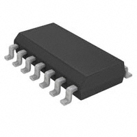
14-SOP Lead-free Package for W83L603G (RoHS Compliable)
•
20-SSOP Lead-free Package for W83L604G (RoHS Compliable)
2.2
Key Specifications
•
Supply Voltage is 3.3V
•
Operating Supply Current is 150 uA typ.
•
Operating Temperature is from 0 °C to 70 °C
- 1 -
Publication Release Date: July, 2008
Revision 1.1
�W83L603G/W83L604G
3. PIN CONFIGURATION
- 2 -
Publication Release Date: July, 2008
Revision 1.1
�W83L603G/W83L604G
4. PIN DESCRIPTION
INts
I/OD12ts
I/O12t
I/O(D)16t
I/O(D)12t
OD12
4.1
TTL level Schmitt-trigger input pin
TTL level bi-directional pin open drain output with 12 mA sink capability and schmitttrigger level input
TTL level bi-directional pin bi-directional output with 12 mA source-sink capability
TTL level bi-directional pin bi-directional (or open drain) output with 16 mA (source-)
sink capability
TTL level bi-directional pin bi-directional (or open drain) output with 12 mA (source-)
sink capability
Open drain output pin with 12 mA sink capability
W83L603G
PIN
SYMBOL
I/O
FUNCTION
1
SCL
INts
2
SDA
I/OD12ts
SMBus bi-directional Data.
3
GP10/LED0
I/O(D)16t
General Purpose I/O. ; LED output
4
GP11/LED1
I/O(D)16t
General Purpose I/O. ; LED output
5
GP12/LED2
I/O(D)16t
General Purpose I/O. ; LED output
6
GP13/LED3
I/O(D)16t
General Purpose I/O. ; LED output
7
VSS
PWR
8
GP14/BEEP
I/O(D)16t
9
GP15 / A2
I/O12t
General Purpose I/O.; Strapping pin for SMBus address bit
2, this pin is internal weak pull down during hardware
reset.
10
GP16 / A1
I/O12t
General Purpose I/O.; Strapping pin for SMBus address bit
1, this pin is internal weak pull down during hardware
reset.
11
GP17 / A0
I/O12t
General Purpose I/O.; Strapping pin for SMBus address bit
0, this pin is internal weak pull down during hardware
reset.
12
INT#
OD12
Auto-generated Interrupt signal when detecting a transition on
GP inputs.
13
RST#
INts
System reset signal input. Low level must be greater than
0.1uS.
14
3VDD
PWR
SMBus Clock.
Power Pin.
General Purpose I/O. ; BEEP output
Power Pin.
- 3 -
Publication Release Date: July, 2008
Revision 1.1
�W83L603G/W83L604G
4.2
W83L604G
PIN
SYMBOL
I/O
FUNCTION
1
SCL
INts
2
SDA
I/OD12ts
SMBus bi-directional Data.
3
GP10/LED0
I/O(D)16t
General Purpose I/O. ; LED output
4
GP11/LED1
I/O(D)16t
General Purpose I/O. ; LED output
5
GP12/LED2
I/O(D)16t
General Purpose I/O. ; LED output
6
GP13/LED3
I/O(D)16t
General Purpose I/O. ; LED output
7
VSS
PWR
8
GP20
I/O(D)12t
General Purpose I/O.
9
GP21
I/O(D)12t
General Purpose I/O.
10
GP22
I/O(D)12t
General Purpose I/O.
11
GP23
I/O(D)12t
General Purpose I/O.
12
GP24
I/O(D)12t
General Purpose I/O.
13
GP25
I/O(D)12t
General Purpose I/O.
14
GP14/BEEP
I/O(D)16t
General Purpose I/O. ; BEEP output
15
GP15 / A2
I/O12t
General Purpose I/O.; Strapping pin for SMBus address bit
2, this pin is internal weak pull down during hardware
reset.
16
GP16 / A1
I/O12t
General Purpose I/O.; Strapping pin for SMBus address bit
1, this pin is internal weak pull down during hardware
reset.
17
GP17 / A0
I/O12t
General Purpose I/O.; Strapping pin for SMBus address bit
0, this pin is internal weak pull down during hardware
reset.
18
INT#
OD12
Auto-generated Interrupt signal when detecting a transition on
GP inputs.
19
RST#
INts
System reset signal input. Low level must be greater than
0.1uS.
20
3VDD
PWR
SMBus Clock.
Power Pin.
Power Pin.
- 4 -
Publication Release Date: July, 2008
Revision 1.1
�W83L603G/W83L604G
5. ARCHITECTURE DESCRIPTION
Register 00h – GP1 input port register
BIT
7
6
5
4
3
2
1
0
R/W
RO
RO
RO
RO
RO
RO
RO
RO
*This register reflects the respective GPI1x pin level.
Register 01h – GP1 output port register
BIT
7
6
5
4
3
2
1
0
R/W
RW
RW
RW
RW
RW
RW
RW
RW
Default
0
0
0
0
0
0
0
0
Register 02h – GP1 Polarity Inversion register
BIT
7
6
5
4
3
2
1
0
R/W
RW
RW
RW
RW
RW
RW
RW
RW
Default
0
0
0
0
0
0
0
0
*Refer to Section 6.2.1 for respective GPO1x pin type implementation.
Register 03h – GP1 input/output configuration register
BIT
7
6
5
4
3
2
1
0
R/W
RW
RW
RW
RW
RW
RW
RW
RW
Default
1
1
1
1
1
1
1
1
*This register configures the respective GPIO1x pin as input mode (“1”; by default) or output mode (“0”).
Register 04h – GP1 output style register
BIT
7
6
5
4
3
2
1
0
R/W
RW
RW
RW
RW
RW
RW
RW
RW
Default
0
0
0
0
0
0
0
0
*This register configures the respective GPO1x pins as level (“0”; by default) or pulse (“1”) output style.
*Set output port register (CR01) to “0” before switch the output style to pulse mode.
Register 05h – GP1 output mode register
BIT
7
6
5
4
3
2
1
0
R/W
RFU
RW
RW
RW
RW
RW
RW
RW
Default
0
0
0
0
0
0
0
0
- 5 -
Publication Release Date: July, 2008
Revision 1.1
�W83L603G/W83L604G
Bit4-Bit0: Configures the respective GPO1x output pads function as Open-drain (“0”; by default) or Pushpull (“1”) mode.
Bit6-5: GP14 / BEEP multi-function configuration register
=11, BEEP frequency = 4KHz; tone = 250 Hz.
=10, BEEP frequency = 2KHz; tone = 10 Hz.
=01, BEEP frequency = 1KHz / 500 Hz; tone= 1 Hz.
=00, BEEP function is disabled on GP14.
Bit7: Reserved for future use.
Register 06h – GP1 interrupt control register
BIT
7
6
5
4
3
2
1
0
R/W
RW
RW
RW
RW
RW
RW
RW
RW
Default
0
0
0
0
0
0
0
0
* This register configures the respective GPI1x pin interrupt control as disable (“0”; by default) or enable
(“1”).
*Clear interrupt status register (CR07) before set to enable.
Register 07h – GP1 interrupt status register
BIT
7
6
5
4
3
2
1
0
R/W
R/clr
R/clr
R/clr
R/clr
R/clr
R/clr
R/clr
R/clr
*The registers are read clear.
*Refer to Section 6.2.3 for implementation.
Register 08h – GP11-GP13 / LED multi-function configuration register
BIT
7
6
5
4
3
2
1
0
R/W
RW
RW
RW
RW
RW
RW
RW
RW
Default
0
0
0
0
0
0
0
0
Bit7-6: GP13 / LED multi-function configuration register
=11, GP13 functions LED output of 2Hz clock, 50% duty cycle.
=10, GP13 functions LED output of 1Hz clock, 50% duty cycle.
=01, GP13 functions LED output of 1/2 Hz clock, 50% duty cycle.
=00, LED function is disabled on GP13. (Default)
Bit5-4: GP12 / LED multi-function configuration register
=11, GP12 functions LED output of 2Hz clock, 50% duty cycle.
=10, GP12 functions LED output of 1Hz clock, 50% duty cycle.
=01, GP12 functions LED output of 1/2 Hz clock, 50% duty cycle.
=00, LED function is disabled on GP12. (Default)
Bit3-2: GP11 / LED multi-function configuration register
=11, GP11 functions LED output of 2Hz clock, 50% duty cycle.
=10, GP11 functions LED output of 1Hz clock, 50% duty cycle.
=01, GP11 functions LED output of 1/2 Hz clock, 50% duty cycle.
=00, LED function is disabled on GP11. (Default)
Bit1-0: GP10 / LED multi-function configuration register
=11, GP10 functions LED output of 2Hz clock, 50% duty cycle.
=10, GP10 functions LED output of 1Hz clock, 50% duty cycle.
=01, GP10 functions LED output of 1/2 Hz clock, 50% duty cycle.
- 6 -
Publication Release Date: July, 2008
Revision 1.1
�W83L603G/W83L604G
=00, LED function is disabled on GP10. (Default)
Register 09h – GP1 input latch data register
BIT
7
6
5
4
3
2
1
0
R/W
RO
RO
RO
RO
RO
RO
RO
RO
Default
0
0
0
0
0
0
0
0
*This register reflects the latch value of GP1x pins during hardware reset.
Register 10h – GP2 input port register (for W83L604G only)
BIT
7
6
NA
R/W
5
4
3
2
1
0
RO
RO
RO
RO
RO
RO
*This register reflects the respective GPI2x pin level.
Register 11h – GP2 output port register (for W83L604G only)
BIT
7
R/W
6
NA
Default
5
4
3
2
1
0
RW
RW
RW
RW
RW
RW
0
0
0
0
0
0
Register 12h – GP2 Polarity Inversion register (for W83L604G only)
BIT
7
R/W
6
NA
Default
5
4
3
2
1
0
RW
RW
RW
RW
RW
RW
0
0
0
0
0
0
*Refer to Section 6.2.1 for respective GPO2x pin type implementation.
Register 13h – GP2 input/output configuration register (for W83L604G only)
BIT
7
R/W
6
NA
Default
5
4
3
2
1
0
RW
RW
RW
RW
RW
RW
1
1
1
1
1
1
*This register configures the respective GPIO2x pin as input mode (“1”; by default) or output mode (“0”).
Register 14h – GP2 output style register (for W83L604G only)
BIT
R/W
Default
7
6
NA
5
4
3
2
1
0
RW
RW
RW
RW
RW
RW
0
0
0
0
0
0
*This register configures the respective GPO2x pins as level (“0”; by default) or pulse (“1”) output style.
*Set output port register (CR11) to “0” before switch the output style to pulse mode.
- 7 -
Publication Release Date: July, 2008
Revision 1.1
�W83L603G/W83L604G
Register 15h – GP2 output mode register (for W83L604G only)
BIT
7
R/W
6
NA
Default
5
4
3
2
1
0
RW
RW
RW
RW
RW
RW
0
0
0
0
0
0
*This register configures the respective GPO2x output pads function as Open-drain (“0”; by default) or
Push-pull (“1”) mode.
Register 16h – GP2 interrupt control register (for W83L604G only)
BIT
7
R/W
6
NA
Default
5
4
3
2
1
0
RW
RW
RW
RW
RW
RW
0
0
0
0
0
0
* This register configures the respective GPI2x pin interrupt control as disable (“0”; by default) or enable
(“1”).
*Clear interrupt status register (CR17) before set to enable.
Register 17h – GP2 interrupt status register (for W83L604G only)
BIT
7
6
NA
R/W
5
4
3
2
1
0
R/clr
R/clr
R/clr
R/clr
R/clr
R/clr
*The registers are read clear.
*Refer to Section 6.2.3 for implementation.
Register 20h – Chip ID (High byte; 95h for W83L604G, 96h for W83L603G)
BIT
7
6
5
4
3
2
1
0
R/W
RO
RO
RO
RO
RO
RO
RO
RO
Default
1
0
0
1
0
1
0/1
1/0
Register 21h – Chip ID (Low byte; 92h)
BIT
7
6
5
4
3
2
1
0
R/W
RO
RO
RO
RO
RO
RO
RO
RO
Default
1
0
0
1
0
0
0
1
- 8 -
Publication Release Date: July, 2008
Revision 1.1
�W83L603G/W83L604G
Register 22h – Global configuration register
BIT
7
6
5
4
3
2
1
0
R/W
WO
RFU
RW
RW
RW
RW
RW
RW
Default
0
0
0
0
0
0
0
0
Bit7: Write “1” to issue a software reset.
Bit6: Reserved for future use.
Bit5: Low power enable bit.
The internal clock generator will shutdown while the bit is set. In the lowpower mode, the functions of SMBus, LED, BEEP, and all signals configured as the pulse mode will
NOT work.
Bit4: Wake-up enable. If the bit is set, low-power enable bit (Bit-5) can be cleared whenever interrupt
event is triggered on GPI pin. To enable the interrupt control register (CR06,CR16) is necessary.
Bit3: Interrupt polarity bit. Refer to Section 7.2.2 for INT pin type implementation.
Bit2: This bit configures the INT signal output as level (“0”; by default) or pulse (“1”) style.
Bit1: GP2 registers mask enable. Set “1” will mask the RST# signal for all GP2 registers. (10h ~ 17h)
Bit0: GP1 registers mask enable. Set “1” will mask the RST# signal for all GP1 registers. (00h ~ 08h)
*Bit1 and Bit0 will not be reset by RST#.
- 9 -
Publication Release Date: July, 2008
Revision 1.1
�W83L603G/W83L604G
6. FUNCTION DESCRIPTIONS
6.1
Access Interface
W83L603G/W83L604G provides a two-wired serial interface which is compliant with SMBusTM Write
Byte and Read Byte protocol.
6.1.1
Write a data into W83L603G/W83L604G register
6.1.2
Read a data from W83L603G/W83L604G register
- 10 -
Publication Release Date: July, 2008
Revision 1.1
�W83L603G/W83L604G
6.2
6.2.1
GPI/O Application Mode:
GPO output
Take Reference Table for GPO Style and Polarity Function.
GPO OUTPUT
STYLE
OUTPUT PORT
REGISTER
OUTPUT VALUE AT PIN
0
1
0
1
0
1
1
0
0
Write 1
Active
1
Write 1
Active
POLARITY
0
Level
1
Pulse
WAVE
*The GPO Pulse Mode output waveform width is 0.5uS.
6.2.2
INT output
Take Reference Table for INT Output Mode and Polarity Function.
INT OUTPUT MODE
Level
Pulse
POLARITY
OUTPUT
0
0
1
1
0
Low Pulse
1
High Pulse
WAVE
*In Level mode, if INT is activated, it will be de-activated when interrupt status registers are read.
*In Pulse mode, interrupt will be activated again unless all enabled interrupt status registers are
read.
*The INT Pulse Mode output waveform width is 0.25uS.
6.2.3
GPI interrupt status
Once a transition occurs at GPI input pins, interrupt status registers (CR07, CR17) will be set. At the
mean time, if interrupt function is enable (CR06, CR16), the INT pin will generate an interrupt
waveform. Reading these interrupt status registers will self clear and reset interrupt. If an interrupt
occurs but never read the interrupt status registers, the interrupt will not be generated again.
- 11 -
Publication Release Date: July, 2008
Revision 1.1
�W83L603G/W83L604G
7. DC AND AC SPECIFICATION
7.1
Absolute Maximum Ratings
PARAMETER
RATING
UNIT
Power Supply Voltage
3.3 ± 10%
V
Input Voltage
3.3 ± 10%
V
Operating Temperature
0 to +70
°C
Storage Temperature
-55 to +150
°C
Note: Exposure to conditions beyond those listed under Absolute Maximum Ratings may adversely affect the life and reliability
of the device.
7.2
Power Supply Current Consumption
(Ta = 0° C to 70° C, VDD = 3.3V ± 10%, VSS = 0V)
PARAMETER
TYPICAL
UNIT
Normal Mode
150
uA
Power Down Mode
10
uA
Note: The Typical value is measured by whole GPIO pins output without load.
7.3
DC Characteristics
(Ta = 0° C to 70° C, VDD = 3.3V ± 10%, VSS = 0V)
IN ts - TTL level schmitt-trigger input pin
PARAMETER
SYM.
Input Low Voltage
V IL
Input High Voltage
V IH
Input High Leakage
I LIH
Input Low Leakage
I LIL
MIN.
TYP.
MAX.
UNIT
CONDITIONS
0.8
V
VDD = 3.3 V
V
VDD = 3.3 V
+10
μA
VIN = VDD
-10
μA
VIN = 0 V
2.0
I/OD 12ts - TTL level bi-direction pin with 12mA sink capability and schmitt-trigger input
Input Low Voltage
V IL
Input High Voltage
V IH
Output Low Voltage
V OL
Input High Leakage
Input Low Leakage
0.8
V
VDD = 3.3 V
V
VDD = 3.3 V
0.4
V
IOL = 12 mA
I LIH
+10
μA
VIN = VDD
I LIL
-10
μA
VIN = 0 V
2.0
- 12 -
Publication Release Date: July, 2008
Revision 1.1
�W83L603G/W83L604G
DC Characteristics , continued.
I/O 12t - TTL level bi-direction pin with 12mA source-sink capability
Input Low Voltage
V IL
Input High Voltage
V IH
Output Low Voltage
V OL
Output High Voltage
V OH
Input High Leakage
I LIH
Input Low Leakage
I LIL
0.8
V
VDD = 3.3 V
V
VDD = 3.3 V
V
IOL = 12 mA
V
IOH = 12 mA
+15
μA
VIN = 3.3 V
-15
μA
VIN = 0 V
2.0
0.4
2.4
I/O(D) 16t - TTL level bi-direction pin with 16mA source-sink capability
Input Low Voltage
V IL
Input High Voltage
V IH
Output Low Voltage
V OL
Output High Voltage
V OH
Input High Leakage
I LIH
Input Low Leakage
I LIL
0.8
V
VDD = 3.3 V
V
VDD = 3.3 V
V
IOL = 16 mA
V
IOH = 16 mA
+10
μA
VIN = 3.3 V
-10
μA
VIN = 0 V
2.0
0.4
2.4
I/O(D) 12t - TTL level bi-direction pin with 12mA source-sink capability
Input Low Voltage
V IL
Input High Voltage
V IH
Output Low Voltage
V OL
Output High Voltage
V OH
Input High Leakage
I LIH
Input Low Leakage
I LIL
0.8
V
VDD = 3.3 V
V
VDD = 3.3 V
V
IOL = 12 mA
V
IOH = 12 mA
+10
μA
VIN = 3.3 V
-10
μA
VIN = 0 V
V
IOL = 12 mA
2.0
0.4
2.4
OD 12 - open-drain output pin with 12mA sink capability
Output Low Voltage
V OL
0.4
- 13 -
Publication Release Date: July, 2008
Revision 1.1
�W83L603G/W83L604G
7.4
AC Characteristics
Serial Bus Timing Diagram
t SCL
tR
t
F
SCL
t HD;STA
t
t SU;STO
SU;DAT
VALID DATA
SDA IN
t HD;DAT
SDA OUT
Serial Bus Timing Diagram
Serial Bus Timing
PARAMETER
SYMBOL
-
MIN.
MAX.
UNIT
SCL clock period
t SCL
10
uS
Start condition hold time
t HD;STA
4.7
uS
Stop condition setup-up time
t SU;STO
4.7
uS
DATA to SCL setup time
t SU;DAT
120
nS
DATA to SCL hold time
t HD;DAT
5
nS
SCL and SDA rise time
tR
1.0
uS
SCL and SDA fall time
tF
300
nS
- 14 -
Publication Release Date: July, 2008
Revision 1.1
�W83L603G/W83L604G
8. PACKAGE DIMENSION OUTLINE
Nuvoton provides two packages for customers thank contain 14-SOP and 20-SSOP.
14L SOP-150mil for W83L603G
- 15 -
Publication Release Date: July, 2008
Revision 1.1
�W83L603G/W83L604G
8
14
c
E
HE
L
7
1
D
0.25
O
A
Y
SEATING PLANE
e
GAUGE PLANE
A1
b
Control demensions are in milmeters .
SYMBOL
A
A1
b
c
E
D
e
HE
Y
L
θ
DIMENSION IN MM
MIN.
MAX.
1.35
1.75
0.10
0.25
0.51
0.33
0.19
0.25
3.80
4.00
8.75
8.55
1.27 BSC
6.20
5.80
0.10
0.40
1.27
0
8
DIMENSION IN INCH
MIN.
MAX.
0.053
0.069
0.010
0.004
0.013
0.020
0.008
0.010
0.150
0.157
0.344
0.337
0.050 BSC
0.228
0.016
0
- 16 -
0.244
0.004
0.050
8
Publication Release Date: July, 2008
Revision 1.1
�W83L603G/W83L604G
20L SSOP-209mil for W83L604G
D
11
20
DTEAIL A
HE
E
10
1
A2
b
A
SEATING PLANE
SEATING PLANE
θ
Y
e
L1
b
SYMBOL
A
A1
A2
b
c
D
E
HE
e
L
L1
Y
θ
A1
DIMENSION IN MM
MIN.
NOM
MAX.
DETAIL A
DIMENSION IN INCH
NOM
MAX.
MIN.
0.079
2.00
0.05
1.65
0.22
0.09
6.90
5.00
7.40
0.55
0
L
1.75
7.20
5.30
7.80
0.65
0.75
1.25
1.85
0.38
0.25
7.50
5.60
8.20
0.002
0.065
0.009
0.004
0.272
0.197
0.291
0.95
0.021
0.10
8
0
0.069
0.283
0.209
0.307
0.073
0.015
0.010
0.295
0.220
0.323
0.0256
- 17 -
0.030
0.050
0.037
0.004
8
Publication Release Date: July, 2008
Revision 1.1
�W83L603G/W83L604G
9. ORDERING INFORMATION
PART NUMBER
PACKAGE TYPE
PRODUCTION FLOW
W83L603G
14-SOP (Leadfree)
Commercial, 0°C to +70°C
W83L604G
20-SSOP (Leadfree)
Commercial, 0°C to +70°C
10. TOP MARKING SPECIFICATION
W83L603G
212345678
524GB
Left line: Chip logo
1st line: W83L603G – the part number for Lead-free product
2nd line: Chip lot no
3rd line: Tracking code 524 G B
524: packages assembled in Year 05’, week 24
G: assembly house ID
B: the IC version
W83L604G
212345678
524GB
Left line: Chip logo
1st line: W83L604G – the part number for Lead-free product
2nd line: Chip lot no
3rd line: Tracking code 524 G B
524: packages assembled in Year 05’, week 24
G: assembly house ID
B: the IC version
- 18 -
Publication Release Date: July, 2008
Revision 1.1
�W83L603G/W83L604G
11. TYPICAL APPLICATION CIRCUIT
3VCC
3VCC 3VCC
R1
10K
3VCC
U1
R2
4.7K
R3
4.7K
SCLK
SDAT
SY STEM_SCLK
SY STEM_SDAT
0
1
2
3
4
5
6
7
SCLK
SDAT
GP10
GP11
GP12
GP13
R4 0
R5
SCLK
3VDD
SDAT
RST#
LED0/GP10
INT#
LED1/GP11 A0/GP17
LED2/GP12 A1/GP16
LED3/GP13 A2/GP15
VSS
BEEP/GP14
32
31
30
29
28
27
26
RST#
RST#
INT#
GP17
GP16
GP15
GP14
C2
C3
10U
0.1U
RST#
OR
C1
1U
SY STEM_RST#
*Connect to System RESET
control output.
W83L603S
C4
C5
10P
10P
*RST# source low level has to greater than 0.1uS width.
SMBus Interface
3VCC
3VCC
R6
4.7K
U2
1
2
3
4
5
6
7
8
9
10
SCLK
SDAT
GP10
GP11
GP12
GP13
GP20
GP21
GP22
SCLK
3VDD
SDAT
RST#
LED0/GP10
INT#
LED1/GP11 A0/GP17
LED2/GP12 A1/GP16
LED3/GP13 A2/GP15
VSS
BEEP/GP14
GP20
GP25
GP21
GP24
GP22
GP23
32
31
30
29
28
27
26
25
24
23
RST#
INT#
GP17
GP16
GP15
GP14
GP25
GP24
GP23
C6
C7
10U
0.1U
INT#
SY STEM_INT#
*Connect to System interrupt input.
W83L604R
3VCC
3VCC
3VCC
BUZZER_VCC
R7
10K
GP17
R8
10K
GP16
A0
R9
10K
PC BEEP
R10
150
GP15
A1
A2
3VCC
SMBUS ADDRESS SELECTION
*Mount the pull up resistor to set
the Address Bit to 1.
R11 330
GP10
1
3VCC
D1
R12 330
2
GP11
1
LED
3VCC
R13 330
GP12
1
3VCC
D3
2
Q1
NPN
GP14
2
LED
BUZZER1
*Example for set the
GP14 to GPO push-pull
type.
AC-1205G
D2
R14 330
GP13
1
D4
2
LED
*The W83L603S/W83L604R GP14 pin default setting
is GP Input , the Buzzer application circuit is
option to selected Buzzer type and GP14 type.
LED
LED GROUP
Size
B
Date:
- 19 -
inbond
Title
WINBOND ELECTRONICS CORP.
Document Number
W83L603S/W83L604R
Monday , July 11, 2005
Sheet
1
Rev
0.1
of
1
Publication Release Date: July, 2008
Revision 1.1
�W83L603G/W83L604G
Important Notice
Nuvoton products are not designed, intended, authorized or warranted for use as components
in systems or equipment intended for surgical implantation, atomic energy control
instruments, airplane or spaceship instruments, transportation instruments, traffic signal
instruments, combustion control instruments, or for other applications intended to support or
sustain life. Furthermore, Nuvoton products are not intended for applications wherein failure of
Nuvoton products could result or lead to a situation wherein personal injury, death or severe
property or environmental damage could occur.
Nuvoton customers using or selling these products for use in such applications do so at their
own risk and agree to fully indemnify Nuvoton for any damages resulting from such improper
use or sales.
- 20 -
Publication Release Date: July, 2008
Revision 1.1
�


 工商网监
湘ICP备2023018690号
工商网监
湘ICP备2023018690号
