UMW
R
SP3232
3.0V TO 5.5V LOW POWER
MULTICHANNEL RS-232 LINE
TRANSCEIVERS USING FOR
0.1 μF EXTERNAL CAPACITORS
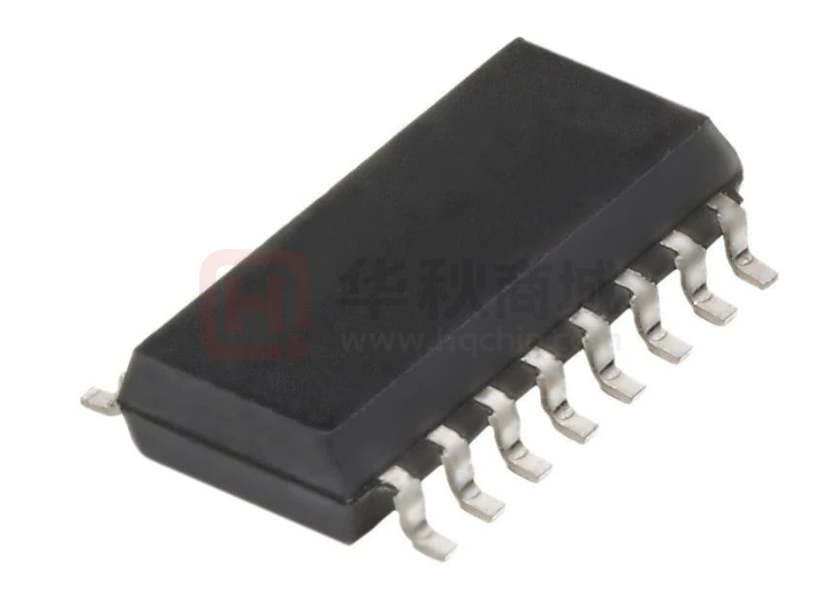
SOP-16
DESCRIPTION
The UMW SP3232EEN has two receivers and two drivers,
and a dual charge-pump circuit. The device meets the
requirements of TIA/EIA-232-F and provides the electrical
interface between an asynchronous communication controller and
the serial-port connector. The charge pump and four small external
capacitors allow operation from a single 3.0V to 5.5V supply.
The device operates at data signaling rates up to 250kbit/s and a
maximum of 35V/μs driver output slew rate.
FEATURES
* Exceeds ±8KV ESD Protection(HBM) for RS-232 I/O Pins
* Meets the Requirements of TIA/EIA-232-F and ITU V.28 Standards
* Operates With 3.0V to 5.5V VCC Supply
* Operates Up To 250kbit/s Data Rate
* Two Drivers and Two Receivers
* External Capacitors 4×0.1μF
* Accepts 5.0V Logic Input With 3.3V Supply
www.umw-ic.com
1
友台半导体有限公司
�UMW
R
SP3232
PIN CONFIGURATION
U MW
SP3232
PIN DESCRIPTION
PIN NO.
1
2
3
4
5
6
7
8
9
10
11
12
13
14
15
16
www.umw-ic.com
PIN NAME
C1+
V+
C1C2+
C2VDOUT2
RIN2
ROUT2
DIN2
DIN1
ROUT1
RIN1
DOUT1
GND
VCC
DESCRIPTION
Positive Terminal of Voltage-Doubler Charge-Pump Capacitor
+5.5V Generated by the Charge Pump
Negative Terminal of Voltage-Doubler Charge-Pump Capacitor
Positive Terminal of Inverting Charge-Pump Capacitor
Negative Terminal of Inverting Charge-Pump Capacitor
-5.5V Generated by the Charge Pump
RS-232 Driver Outputs
RS-232 Receiver Inputs
TTL/CMOS Receiver Outputs
TTL/CMOS Driver Inputs
TTL/CMOS Driver Inputs
TTL/CMOS Receiver Outputs
RS-232 Receiver Inputs
RS-232 Driver Outputs
Ground
+3.0V to +5.5V Supply Voltage
2
友台半导体有限公司
�UMW
R
SP3232
BLOCK DIAGRAM
DIN1 11
14 DOUT1
DIN2 10
7
DOUT2
UMW
SP3232
13 RIN1
ROUT1 12
5kΩ
ROUT2
9
8
RIN2
5kΩ
www.umw-ic.com
3
友台半导体有限公司
�UMW
R
SP3232
ABSOLUTE MAXIMUM RATING [Over operating free-air temperature range (unless otherwise noted)]
PARAMETER
SYMBOL
RATINGS
UNIT
Supply Voltage Range
VCC
-0.3 ~ +6.0
V
Positive Output Supply Voltage Range (Note 2)
V+
-0.3 ~ +7.0
V
Negative Output Supply Voltage Range (Note 2)
V+0.3 ~ -7.0
V
Supply Voltage Difference (Note 2)
V+ - V+13
V
Drivers
-0.3 ~ +6.0
V
Input Voltage
VIN
Receivers
-25 ~ +25
V
Drivers
-13.2 ~ +13.2
V
Output Voltage
VOUT
Receivers
-0.3 ~ VCC+0.3
V
Operating Virtual Junction Temperature
TJ
+150
°C
Storage Temperature
TSTG
-65 ~ + 150
°C
Notes: 1. Absolute maximum ratings are those values beyond which the device could be permanently damaged.
Absolute maximum ratings are stress ratings only and functional device operation is not implied.
2. All voltages are with respect to network GND.
THERMAL DATA
PARAMETER
Junction to Ambient
SOP-16
SYMBOL
RATING
UNIT
θJA
105
°C/W
RECOMMENDED OPERATING CONDITIONS (See Note & Table 1)
PARAMETER
SYMBOL
Supply Voltage
VCC
Driver and Control High-level Input
Voltage
VIH
TEST CONDITIONS
VCC=3.3V
VCC=5.0V
VCC=3.3V
DIN
VCC=5.5V
MIN
3.0
4.5
2.0
2.4
TYP
3.3
5.0
MAX
3.6
5.5
V
Driver and Control Low-level Input
VIL
DIN
0.8
Voltage
Driver and Control Input Voltage
VIN
DIN
5.5
Receiver Input Voltage
VRIN
-25
25
0
70
Operating Free-Air Temperature
TA
Notes: Test conditions are C1~C4=0.1μF at VCC=3.3V±0.3V; C1=0.047μF, C2~C4=0.33μF at VCC=5.0V±0.5V.
www.umw-ic.com
4
UNIT
V
V
V
V
V
°C
友台半导体有限公司
�UMW
R
SP3232
ELECTRICAL CHARACTERISTICS [(over recommended ranges of supply voltage and operating
free-air temperature (unless otherwise noted) (see Note 3 & Table 1)]
PARAMETER
Supply Current
DRIVER SECTION
High-Level Output Voltage
Low-Level Output Voltage
High-Level Input Current
Low-Level Input Current
Short-Circuit Output Current
(Note 2)
Output Resistance
RECEIVER SECTION
High-Level Output Voltage
Low-Level Output Voltage
Positive-Going Input Threshold
Voltage
SYMBOL
TEST CONDITIONS
ICC
No load
VOH
VOL
IOH
IOL
DOUT at RL=3kΩ to GND, DIN=GND
DOUT at RL=3kΩ to GND, DIN=VCC
VI=VCC
VI at GND
VCC=3.6V, VOUT=0V
VCC=5.5V, VOUT=0V
VCC, V+ and V- =0V, VOUT=±2.0V
IOS
rO
MIN
+5.0
-5.0
300
TYP
(Note 1)
0.3
+5.4
-5.4
±0.01
±0.01
±35
±35
10M
MAX
UNIT
1.0
mA
V
V
μA
μA
mA
mA
Ω
±1
±1
±60
±60
VOH
VOL
IOH=-1.0mA
V
VCC-0.6V VCC- 0.1V
IOL=1.6mA
0.4
V
VCC=3.3V
1.5
2.4
V
VIT+
VCC=5.0V
1.8
2.4
V
Negative-Going Input
VCC=3.3V
0.6
1.2
V
VITThreshold Voltage
VCC=5.0V
0.8
1.5
V
Input Hysteresis
VHYS
VIT+~VIT0.3
V
Input Resistance
RI
VI=±3.0V~±25V
3
5
7
kΩ
Notes: 1. All typical values are at VCC=3.3V or VCC=5.0V, and TA=25°C.
2. Short-circuit durations should be controlled to prevent exceeding the device absolute power-dissipation
ratings, and not more than one output should be shorted at a time.
3. Test conditions are C1~C4=0.1μF at VCC=3.3V±0.3V; C1=0.047μF, C2~C4=0.33μF at VCC=5.0V±0.5V.
4. Pulse skew is defined as |tPLH−tPHL| of each channel of the same device.
SWITCHING CHARACTERISTICS
[over recommended ranges of supply voltage and operating
free-air temperature (unless otherwise noted) (see Note 3 and Table 1)]
PARAMETER
SYMBOL
TEST CONDITIONS
tSK(p)
CL=1000pF, RL=3kΩ, One Driver
Switching
CL=220pF~2500pF, RL =3kΩ~7kΩ
RL =3kΩ~7kΩ, CL=220pF~1000pF
VCC=3.3V
CL=220pF~2500pF
MIN
TYP
(Note 1)
MAX
UNIT
250
Kbit/s
DRIVER SECTION
Maximum Data Rate
Pulse Skew (Note 4)
Slew Rate, Transition Region
SR(tr)
120
300
5
3
ns
35
35
V/μs
RECEIVER SECTION
Propagation Delay Time, LowtPLH
CL=150pF
300
ns
to High-Level Output
Propagation Delay Time, HightPHL
CL=150pF
300
ns
to Low-Level Output
Output Enable Time
tEN
CL=150pF, RL=3kΩ
200
ns
Output Disable Time
tDIS
CL=150pF, RL=3kΩ
200
ns
Pulse Skew (Note 4)
tSK(P)
|tPLH−tPHL|
300
ns
Notes: 1. All typical values are at VCC=3.3V or VCC=5.0V, and TA=25°C.
2. Short-circuit durations should be controlled to prevent exceeding the device absolute power-dissipation
ratings, and not more than one output should be shorted at a time.
3. Test conditions are C1~C4=0.1μF at VCC=3.3V±0.3V; C1=0.047μF, C2~C4=0.33μF at VCC=5.0V±0.5V.
4. Pulse skew is defined as |tPLH−tPHL| of each channel of the same device.
www.umw-ic.com
5
友台半导体有限公司
�UMW
R
SP3232
TYPICAL APPLICATION CIRCUIT
UMW
SP3232
Table1. Typical Operating Circuit and Capacitor Values
VCC (V)
3.0~3.6
3.15~3.6
4.5~5.5
3.0~5.5
www.umw-ic.com
C1 (µF)
0.22
0.1
0.047
0.22
C2, C3, C4 (µF)
0.22
0.1
0.33
1.0
6
CBYPASS (µF)
0.22
0.1
0.047
0.22
友台半导体有限公司
�UMW
R
SP3232
PACKAGE: SOP-16
UNIT: mm
L
SYMBOL
MILLIMETER
MIN
NOM MAX
A
E
E1
b
e
c
1.80
A1
0.10
0.15
0.25
A2
1.25
1.45
1.65
b
0.33
0.51
c
0.17
0.25
D
9.50
E
5.80
E1
3.70
e
L
10.20
6.00
6.20
4.10
1.27BSC
0.45
0.60
0.80
D
A2 A
A1
ORDERING INFORMATION
Ordering Number
Package
Baseqty
UMW SP3232EEN
SOP-16
2500
www.umw-ic.com
7
Packing
Tape and reel
友台半导体有限公司
�
很抱歉,暂时无法提供与“SP3232EEN”相匹配的价格&库存,您可以联系我们找货
免费人工找货- 国内价格
- 5+0.75330
- 20+0.73948
- 100+0.71183


 工商网监
湘ICP备2023018690号
工商网监
湘ICP备2023018690号
