FP5501
fitipower integrated technology lnc.
Low-saturation, Low-voltage 2 Channels
Bi-directional Motor Driver
Description
Features
The FP5501 is a monolithic IC for low-saturation
bi-directional low cost and high efficiency miniature
two DC motor or stepper motor applications, such as
driving shutter (DC actuator), auto-focus (stepper
motor), iris (stepper motor) and accurate zoom
(stepper motor) on cameras, vibration on mobile
phone and other motor applications on portable
devices.
Low Voltage Operation (VCC Min=1.8V)
Full- and Half-Stepping Capability
Low Saturation Voltage (Upper + Low Transistor
Residual Voltage; 0.46V typ. at 400mA)
Low Input Current
Low Operating Current, Sleep Mode with Zero
Current Drain
Dead-Zone Protection
High Output Sinking and Driving Capability
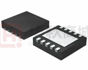
Small, Thin, Highly Reliable Package (TDFN-10)
Available COB Package
Thermal Shutdown Protection
Applications
Stepper Motor
DSC
Camera Module
Motor Application on Portable Device
Pin Assignments
Ordering Information
WD Package (TDFN-10)(3mm×3mm)
FP5501□□□
TR: Tape/Reel
Blank: Tube
VCC
1
10 VOUT4
VIN4
2
9
VOUT3
VIN3
3
8
VOUT1
VIN1
4
7
VOUT2
VIN2
5
6
VSS
FP5501
P: Green
Package Type
WD: TDFN-10 (3mm×3mm)
CH: CHIP
Figure 1. Pin Assignment of FP5501 (Top View)
FP5501-1.7-JAN-2013
1
�fitipower integrated technology lnc.
FP5501
Block Diagram & Application Circuit
1. Shutter & Iris application
Figure 1a. Dual DC Motor Application
2. Stepping motor for 1-2 phase excitation
Figure 1b. Stepper Motor Application
3. Typical single dc motor control (paralleled outputs)
Figure 1c. Single (paralleled) DC Motor Application
FP5501-1.7-JAN-2013
2
�FP5501
fitipower integrated technology lnc.
Functional Pin Description
Pin No.
Pin Name
Pin Function
1
VCC
Power supply pin.
2
VIN4
Input pin.
3
VIN3
Input pin.
4
VIN1
Input pin.
5
VIN2
Input pin.
6
VSS
Ground pin.
7
VOUT2
Output sinking or driving current pin.
8
VOUT 1
Output driving or sinking current pin.
9
VOUT 3
Output sinking or driving current pin.
10
VOUT 4
Output driving or sinking current pin.
Block Diagram
Figure 2. Block Diagram of FP5501
FP5501-1.7-JAN-2013
3
�FP5501
fitipower integrated technology lnc.
Absolute Maximum Ratings
● VCC to VSS ----------------------------------------------------------------------------------------------- -0.3V to +5.5V
● VIN and VOUT to VSS ---------------------------------------------------------------------------------- -0.3V to +6V
● Output Current per Channel *1 ----------------------------------------------------------------------- 0mA to 400mA
● Continuous Power Dissipation ------------------------------------------------------------------------ 486mW
● Junction Temperature ----------------------------------------------------------------------------------- +150°C
● Storage Temperature Range -------------------------------------------------------------------------- -65°C to +150°C
● Lead Temperature (Soldering, 10sec.) ------------------------------------------------------------- 260°C
● ESD (Human Body Model) *2 ------------------------------------------------------------------------- 4000V
*1: Output current rating may be limited by ambient temperature and heat sinking.
exceed the specified.
Under any set of conditions, do not
*2: ESD caution: ESD (electrostatic discharge) sensitive device. Electrostatic charges as high as 4000V readily
accumulate on the human body and test equipment and can discharge without detection. Although this product
features proprietary ESD protection circuitry, permanent damage may occur on devices subjected to high energy
electrostatic discharges. Therefore, proper ESD precautions are recommended to avoid performance degradation or
loss of functionality.
Recommended Operating Conditions
● Supply Voltage VCC to VSS -------------------------------------------------------------------------- 1.8V to 5.5V
● Maximum Output Drop Voltage (400mA Output Current) -------------------------------------- 0.46V
● Operation Temperature Range ----------------------------------------------------------------------- -40°C to +125°C
FP5501-1.7-JAN-2013
4
�FP5501
fitipower integrated technology lnc.
Electrical Characteristics
(Unless otherwise noted, TA=25°C & VCC=3V)
Parameter
Symbol
Supply Voltage
Conditions
VCC
Supply Current
( ICC + ISS)
Min.
Typ.
Max.
Unit
1.8
3.0
5.5
V
ICC0
VVIN1, VIN2, VIN3, VIN4=0V
-
0.1
10
μA
ICC1
VVIN1, VIN2, VIN3, VIN4 ≠0V
-
0.15
0.4
mA
1.5
-
VIN 1 / VIN 2 / VIN3 / VIN4 Input Terminal ( TJ=25°C)
Input Voltage “H”
VINH
Input Voltage “L”
VINL
Input Voltage Hysteresis
VHsy
Input Current “H”
IINH
Input Current “L”
IINL
V
-
0.4
V
-
0.42
-
V
VIN=VCC
-
-
5
μA
VIN=0V
-
-
5
μA
VOUT1 / VOUT 2 / VOUT 3 / VOUT 4 Output Terminal (TJ=25°C)
VSAT1
IOUT=200mA
-
0.22
0.4
V
VSAT2
IOUT=400mA
-
0.46
0.7
V
Protection Temperature
TTSD
VVIN1, VIN2, VIN3, VIN4=H
-
150
-
°C
Temperature Hysteresis
THsy
VVIN1, VIN2, VIN3, VIN4=H
-
25
-
°C
Output Voltage
(Upper + Lower)
Thermal Protection Circuit
Truth Table
VIN1 or 3
VIN2 or 4
VOUT1 or 3
VOUT2 or 4
Low
Low
OFF
OFF
Standby
High
Low
High
Low
Forward
Low
High
Low
High
Reverse
High
High
---
---
FP5501-1.7-JAN-2013
Mode
Keep the Previous Mode (Forward / Reverse)
5
�FP5501
fitipower integrated technology lnc.
Truth Table Test Waves
Figure 3. Truth Table Test Waves
Characteristic Performance Curve
Figure 4a. VSAT vs. IOUT
FP5501-1.7-JAN-2013
Figure 4b. ISS vs. VCC
6
�FP5501
fitipower integrated technology lnc.
Motor Operation Truth Table
INX *1
VOUT1*2
VOUT2
VOUT3
VOUT4
Function
Stepper Motor
VIN1
VIN2
VIN3
VIN4
VOUT1*2
VOUT2
VOUT3
VOUT4
Full-Stepping
Half-Stepping
0
0
0
0
OFF
OFF
OFF
OFF
Sleep Mode
Sleep Mode
1
0
1
0
H
L
H
L
Step1 *3
Step1
0
0
1
0
OFF
OFF
H
L
Step1_1 *4
Step2
0
1
1
0
L
H
H
L
Step2
Step3
0
1
0
0
L
H
OFF
OFF
Step2_1
Step4
0
1
0
1
L
H
L
H
Step3
Step5
0
0
0
1
OFF
OFF
L
H
Step3_1
Step6
1
0
0
1
H
L
L
H
Step4
Step7
1
0
0
0
H
L
OFF
OFF
Step4_1
Step8
DC Motor (Dual)
VIN1 or VIN3
VIN2 or VIN4
VOUT1*2
VOUT2
VOUT3
VOUT4
Function
0
0
OFF
OFF
OFF
OFF
Sleep Mode
1
0
H
L
H
L
Forward
0
1
L
H
L
H
Reverse
1
1
--
--
--
--
Keep the previous mode
(Forward/Reverse)
DC Motor (Single, Paralleled)
VIN1 or VIN3
VIN2 or VIN4
VOUT1*2
VOUT2
VOUT3
VOUT4
Function
0
0
OFF
OFF
OFF
OFF
Sleep Mode
1
0
H
L
H
L
Forward
0
1
L
H
L
H
Reverse
1
1
--
--
--
--
Keep the previous mode
(Forward/Reverse)
*1: 0=logic low, VinxVIH (min.).
*2: H=voltage high, source driver on; L=voltage low, sink driver on.
*3: Two phase on stepper motor drive
*4: One phase on stepper motor drive
FP5501-1.7-JAN-2013
7
�fitipower integrated technology lnc.
FP5501
Function Description
Device Operation
The FP5501 is a dual full-bridge low voltage motor driver capable of operating one stepper motor or up to two
dc motors. MOSFET output stages substantially reduce the voltage drop and the power dissipation of the
outputs of the FP5501 compared to typical drivers with bipolar transistors. Internal circuit protection includes
thermal shutdown with hysteresis and crossover current protection. The FP5501 is designed for portable
applications with a power-off (sleep mode) current of 100nA typical, and an operating voltage of 1.8V to 5.5V.
The FP5501 logic inputs are 3 to 5V logic compatible.
In conditions where the logic supply voltage drops below 1.8V, both the sink and the source voltage drop will
increase beyond the specified values. In extreme cases, no power will be delivered to the motors. However,
the device will not be damaged.
In stepping operation, the device can drive in either full- or half-step mode. The stepping mode is set by the
signal pattern on the Inx terminals, as shown in the stepping timing diagrams.
Sleep Mode
Pulling all inputs to 0.4V or less, sends the FP5501 to sleep mode, during which it draws 100nA typical.
Thermal Shutdown
The FP5501 will disable the outputs if the junction temperature reaches 150ºC. When thermal shutdown is
entered, after the junction temperature drops 15ºC, the outputs will be re-enabled.
FP5501-1.7-JAN-2013
8
�fitipower integrated technology lnc.
FP5501
Application Notes
Figure 5a. Typical stepper motor control application
Figure 5b. Full step mode timing chart (two phase on)
Figure 5c. Full step mode timing chart (one phase on)
FP5501-1.7-JAN-2013
9
�fitipower integrated technology lnc.
FP5501
Application Notes (Continued)
Figure 5d. Half step mode timing chart
Figure 6. Typical dual dc motor control application.
Either IN1 or IN2 and be used to drive OUT1 and OUT2.
FP5501-1.7-JAN-2013
Either IN3 or IN4 and be used to drive OUT3 and OUT4.
10
�fitipower integrated technology lnc.
FP5501
Application Notes (Continued)
Figure 7. Typical single dc motor control application (paralleled outputs).
Figure 8. Typical dual dc motor control application (timing chart)
The power dissipated by the IC varies widely with the supply voltage, the output current, and loading. It is
important to ensure the application does not exceed the allowable power dissipation of the IC package. The
recommended motor driver power dissipation versus temperature is depicted as follows:
FP5501-1.7-JAN-2013
11
�FP5501
fitipower integrated technology lnc.
Outline Information
TDFN-10 3mm x 3mm (pitch 0.5 mm) Package (Unit: mm)
SYMBOLS
UNIT
DIMENSION IN MILLIMETER
MIN
MAX
A
0.70
0.80
A1
0.00
0.05
A2
0.18
0.25
D
2.95
3.05
E
2.95
3.05
a
0.30
0.50
b
0.18
0.30
e
0.45
0.55
D1
2.20
2.70
E1
1.40
1.75
Carrier Dimensions
Life Support Policy
Fitipower’s products are not authorized for use as critical components in life support devices or other medical systems.
FP5501-1.7-JAN-2013
12
�
很抱歉,暂时无法提供与“FP5501WDPTR”相匹配的价格&库存,您可以联系我们找货
免费人工找货- 国内价格
- 1+1.81250
- 30+1.75000
- 100+1.62500
- 500+1.50000
- 1000+1.43750


 工商网监
湘ICP备2023018690号
工商网监
湘ICP备2023018690号
