FP6397
High Efficiency 1MHz 2A
Synchronous Step Down Converter
Description
Features
The FP6397 is a high efficiency, high frequency
synchronous DC-DC step-down converter. The
100% duty cycle feature provides low dropout
operation, extending battery life in portable systems.
The internal synchronous switch increases efficiency
and eliminates the need for external Schottky diode.
At shutdown mode, the input supply current is less
than 1µA.
The FP6397 fault protection includes over current
protection, short circuit protection, UVLO and
thermal shutdown. The Internal soft-start function
prevents inrush current at turn-on.
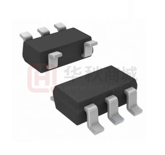
The FP6397 is offered in SOT-23-5 and SOT-23-6
Packages.
2.5V~6V Input Voltage Range
0.6V Reference Voltage
2A Output Current
Low RDS(ON) for Internal Switch (Top/Bottom):
140/90mΩ
1MHz Switching Frequency
Internal Soft-Start Limits the Inrush Current
Internal Compensation Function
100% Dropout Operation
Power Good Indicator Output (SOT-23-6 Only)
Input Over Voltage Protection
Over Current Protection
Hiccup Short Circuit Protection
Over Temperature Protection with Auto Recovery
RoHS Compliant and Halogen Free
Applications
Pin Assignments
Ordering Information
FP6397□
S5 Package (SOT-23-5)
FB
VIN
5
4
1
Set Top Box
LCD TV & Tablet
AP Router & WiFi Dongle
3.5G & 4G Dongle
USB3.0 & SSD storage
2
Package Type
S5: SOT-23-5
S6: SOT-23-6
3
EN GND LX
S6 Package (SOT-23-6)
FB
PG VIN
6
5
4
1
2
3
EN GND LX
SOT-23-5 Marking
Part Number
Product Code
FP6397S5
FV9
SOT-23-6 Marking
Part Number
Product Code
FP6397S6
FW1
Figure 1. Pin Assignment of FP6397
FP6397-Preliminary 0.3-AUG-2019
1
�FP6397
Typical Application Circuit
Figure 2. Schematic Diagram
VIN=5V, the recommended BOM list is as below.
VOUT
3.3V
2.5V
1.8V
1.5V
1.2V
1.05V
C1
10μF MLCC
10μF MLCC
10μF MLCC
10μF MLCC
10μF MLCC
10μF MLCC
R1
453kΩ
316kΩ
200kΩ
150kΩ
100kΩ
75kΩ
R2
100kΩ
100kΩ
100kΩ
100kΩ
100kΩ
100kΩ
L1
2.2μH
2.2μH
1.8μH
1.5μH
1.5μH
1.2μH
C2
10μF MLCC
10μF MLCC
10μF MLCC
10μF MLCC
10μF MLCC
10μF MLCC
Table 1. Recommended Component Values
FP6397-Preliminary 0.3-AUG-2019
2
�FP6397
Functional Pin Description
Pin Name
Pin No.
(SOT-23-6)
Pin No.
(SOT-23-5)
Pin Function
EN
1
1
Enable control pin. Pull high to turn the IC on, and pull low to disable the IC. Don’t leave
this pin floating.
GND
2
2
Ground pin.
LX
3
3
Power switching node. Connect an inductor to the drains of internal high side PMOS
and low side NMOS.
VIN
4
4
Power supply input pin. Placed input capacitors as close as possible from VIN to GND
to avoid noise influence.
PG
5
--
Open drain power good output pin.
FB
6
5
Voltage feedback input pin. Connect FB and VOUT with a resistive voltage divider. This IC
senses feedback voltage via FB and regulates it at 0.6V.
Block Diagram
PG
(SOT-23-6)
EN
VIN
2M
Power Good
Enable
Control
VIN
OVP
UVLO
Slope
Compensation
90%
VREF
FB
1
COMP
Control Logic
EA
VREF
Soft
Start
OSC
OTP
Driver
Logic
X
LX
COMP
GND
Figure 3. Block Diagram of FP6397
FP6397-Preliminary 0.3-AUG-2019
3
�FP6397
Absolute Maximum Ratings (Note 1)
● VIN to GND ------------------------------------------------------------------------------------------------- -0.3V to +6.5V
● LX to GND --------------------------------------------------------------------------------------------------- -0.3V to (VIN +0.3V)
● EN, FB, PG to GND --------------------------------------------------------------------------------------- -0.3V to VIN
● Package Thermal Resistance, (θJA)
(Note 2)
SOT-23-5 ---------------------------------------------------------------------------------------- 250°C/W
SOT-23-6 ---------------------------------------------------------------------------------------- 250°C/W
● Package Thermal Resistance, (θJC)
SOT-23-5 ---------------------------------------------------------------------------------------- 130°C/W
SOT-23-6 ---------------------------------------------------------------------------------------- 110ºC/W
● Maximum Junction Temperature (T J) ----------------------------------------------------------------- +150°C
● Lead Temperature (Soldering, 10sec.) --------------------------------------------------------------- +260°C
● Storage Temperature (TS) ------------------------------------------------------------------------------- -65°C to +150°C
Note 1: Stresses beyond this listed under “Absolute Maximum Ratings" may cause permanent damage to the device.
Note 2: θJA is measured at 25°C ambient with the component mounted on a high effective thermal conductivity test board of JEDEC-51-7.
The thermal resistance greatly varies with layout, copper thickness, number of layers and PCB size.
Recommended Operating Conditions (Note 3)
● Supply Voltage (VIN) ------------------------------------------------------------------------------------------- +2.5V to +6V
● Junction Temperature Range ------------------------------------------------------------------------------- -40°C to +125°C
● Operation Temperature Range (T OPR) -------------------------------------------------------------------- -40°C to +85°C
Note 3: The device is not guaranteed to function outside its operating conditions.
FP6397-Preliminary 0.3-AUG-2019
4
�FP6397
Electrical Characteristics
(VIN=5V, TA=25°C, unless otherwise specified.)
Parameter
Symbol
Input Supply Voltage
Conditions
VIN
Input Over Voltage Protection
Min
2.5
VIN OVP
Shutdown Current
ISHDN
Quiescent Current
Iq
Reference Voltage
VREF
FB Input Leakage Current
IFB
Typ
Max
Unit
6.0
V
6.3
EN=GND
0.1
VFB=0.65V, IOUT=0A
40
0.588
VFB=VIN
V
1
μA
μA
0.6
0.612
V
0.01
1
µA
P-Channel MOSFET On-Resistance
(Note 4)
RDS(ON)
140
mΩ
N-Channel MOSFET On-Resistance
(Note 4)
RDS(ON)
90
mΩ
2.7
A
P-Channel Current Limit
(Note 4)
ILIM
2.2
EN High-Level Input Voltage
VEN(H)
1.5
EN Low-Level Input Voltage
VEN(L)
Under Voltage Lockout Voltage
UVLO
2.4
V
UVLO Hysteresis
VHYS
0.2
V
Oscillation Frequency
FOSC
V
0.4
IOUT=300mA
0.8
Minimum On Time
1.0
50
Maximum Duty Cycle
100
1.2
V
MHz
ns
%
PG Rising Threshold
VPG (H)
VFB Rising
90
%
PG Low Threshold
VPG (L)
VFB falling
85
%
PG Sink Current
IPG
VPG=0.1V
1
mA
Internal Soft-Start Time
TSS
1
ms
100
Ω
150
°C
VOUT Discharge Resistance
Thermal Shutdown Temperature
(Note 4)
TSD
Note 4: Guarantee by design.
FP6397-Preliminary 0.3-AUG-2019
5
�FP6397
Typical Performance Curves
VIN=5V, VOUT=1.2V, C1=10μF, C2=10μF, L1=1.5μH, TA=+25°C, unless otherwise noted.
VOUT=3.3V
100
100
90
80
70
60
90
80
50
40
30
20
10
0
0.01
Efficiency(%)
Efficiency(%)
VOUT=1.2V
VIN=3.3V
70
60
50
40
30
VIN=4.2V
20
VIN=5.0V
0.1
1
VIN=5.0V
10
0
0.01
10
Load Current (A)
-40 -30 -20 -10 0 10 20 30 40 50 60 70 80 90
10
1.10
1.08
1.06
1.04
1.02
1.00
0.98
0.96
0.94
0.92
0.90
-40 -30 -20 -10 0 10 20 30 40 50 60 70 80 90
Ambient Temperature (℃)
Ambient Temperature (℃)
Figure 6. Feedback Voltage vs. Temperature
IOUT=0A
1
Figure 5. Efficiency vs. Load Current
Frequency (MHz)
Feedback Voltage (V)
Figure 4. Efficiency vs. Load Current
0.65
0.64
0.63
0.62
0.61
0.60
0.59
0.58
0.57
0.56
0.55
0.1
Load Current (A)
Figure 7. Frequency vs. Temperature
IOUT=2A
VIN
2V/div.
VIN
2V/div.
VLX 2V/div.
VLX
2V/div.
VOUT 500mV/div.
VOUT 500mV/div.
ILX
200mA/div.
ILX
1A/div.
4ms/div.
4ms/div.
Figure 8. Power On through VIN Waveform
Figure 9. Power On through VIN Waveform
FP6397-Preliminary 0.3-AUG-2019
6
�FP6397
Typical Performance Curves (Continued)
VIN=5V, VOUT=1.2V, C1=10μF, C2=10μF, L1=1.5μH, TA=+25°C, unless otherwise noted.
IOUT=2A
IOUT=0A
VIN
VLX
2V/div.
VIN
2V/div.
VLX
2V/div.
2V/div.
VOUT 500mV/div.
VOUT 500mV/div.
ILX
ILX
200mA/div.
20ms/div.
1A/div.
20ms/div.
Figure 10. Power Off through VIN Waveform
IOUT=0A
Figure 11. Power Off through VIN Waveform
IOUT=2A
VEN
5V/div.
VEN
5V/div.
VLX
2V/div.
VLX
2V/div.
VOUT
500mV/div.
VOUT
500mV/div.
ILX
200mA/div.
ILX
1A/div.
4ms/div.
4ms/div.
Figure 12. Power On through EN Waveform
Figure 13. Power On through EN Waveform
IOUT=0A
IOUT=2A
VEN
5V/div.
VEN
5V/div.
VLX
2V/div.
VLX
2V/div.
VOUT
500mV/div.
VOUT
500mV/div.
ILX
200mA/div.
ILX
1A/div.
4ms/div.
20μs/div.
Figure 14. Power Off through EN Waveform
Figure 15. Power Off through EN Waveform
FP6397-Preliminary 0.3-AUG-2019
7
�FP6397
Typical Performance Curves (Continued)
VIN=5V, VOUT=1.2V, C1=10μF, C2=10μF, L1=1.5μH, TA=+25°C, unless otherwise noted.
IOUT=2A
IOUT=0A
VLX
VLX
2V/div.
VOUT 50mV/div.
VOUT 50mV/div.
ILX
ILX
2V/div.
1A/div.
200mA/div.
20ms/div
1μs/div
Figure 16. Steady State Waveform
Figure 17. Steady State Waveform
IOUT=0.2A to 2A
VOUT 100mV/div.
ILX
1A/div.
80μs/div.
Figure 18. Load Transient Waveform
FP6397-Preliminary 0.3-AUG-2019
8
�FP6397
Function Description
The FP6397 is a high efficiency, internal
compensation and constant frequency current mode
step-down synchronous DC/DC regulator. It has
integrated high-side (140mΩ, typ) and low-side
(90mΩ, typ) power switches, and provides 2A
continuous load current. It regulates input voltage
from 2.5V to 6V, and down to an output voltage as
low as 0.6V.
Control Loop
Slope compensated current mode PWM control
provides stable switching and cycle-by-cycle current
limit for superior load, line response, protection of the
internal main switch and synchronous rectifier. The
FP6397 switches at a constant frequency (1MHz) and
regulates the output voltage. During each cycle, the
PWM comparator modulates the power transferred to
the load by changing the inductor peak current based
on the feedback error voltage. During normal
operation, the main switch is turned on for a certain
time to ramp the inductor current at each rising edge
of the internal oscillator, and switched off when the
peak inductor current is above the error voltage.
When the main switch is off, the synchronous rectifier
will be turned on immediately and stay on until next
cycle starts.
Enable
The FP6397 EN pin provides digital control to turn
on/off the regulator. When the voltage of EN exceeds
the threshold voltage, the regulator will start the soft
start function. If the EN pin voltage is below the
shutdown threshold voltage, the regulator will turn
into the shutdown mode and the shutdown current
will be smaller than 1μA. For auto start-up operation,
connect EN to VIN.
Soft Start
The FP6397 employs internal soft start function to
reduce input inrush current during start up. The
internal soft start time will be 1ms.
Short Circuit Protection
The FP6397 provides short circuit protection
function to prevent the device damaged from short
condition. When the short condition occurs and the
feedback voltage drops lower than 40% of the
regulation level, the oscillator frequency will be
reduced and hiccup mode will be triggered to
prevent the FP6397 from overheating during the
extended short condition. Once the short condition
is removed, the frequency and current limit will
return to normal.
Over Current Protection
The FP6397 over current protection function is
implemented by using cycle-by-cycle current limit
architecture. The inductor current is monitored by
measuring the high-side MOSFET series sense
resistor voltage. When the load current increases,
the inductor current will also increase. When the
peak inductor current reaches the current limit
threshold, the output voltage will start to drop.
When the over current condition is removed, the
output voltage will return to the regulated value.
Over Temperature Protection
The FP6397 incorporates an over temperature
protection circuit to protect itself from overheating.
When the junction temperature exceeds the thermal
shutdown threshold temperature, the regulator will
be shutdown. And the hysteretic of the over
temperature protection is 30°C (typ).
PG Signal Output
PG pin is an open-drain output and requires a pull
up resistor. PG is actively held low in soft-start,
standby and shutdown. It is released when the
output voltage rises above 90% of nominal
regulation point.
Under Voltage Lockout
When the FP6397 is power on, the internal circuits
will be held inactive until VIN voltage exceeds the
UVLO threshold voltage. And the regulator will be
disabled when VIN is below the UVLO threshold
voltage. The hysteretic of the UVLO comparator is
200mV (typ).
FP6397-Preliminary 0.3-AUG-2019
9
�FP6397
Application Information
Output Voltage Setting
The output voltage VOUT is set by using a resistive
divider from the output to FB. The FB pin regulated
voltage is 0.6V. Thus the output voltage is:
V
T =0. V
1+
Output Capacitor Selection
R1
R2
Table 2 lists recommended values of R1 and R2 for
most used output voltage.
Table 2
A low ESR capacitor is required to keep the noise
minimum. Ceramic capacitors are better, but
tantalum or low ESR electrolytic capacitors may
also suffice.
Recommended Resistance Values
VOUT
R1
R2
3.3V
453kΩ
100kΩ
2.5V
316kΩ
100kΩ
1.8V
200kΩ
100kΩ
1.5V
150kΩ
100kΩ
1.2V
100kΩ
100kΩ
The output capacitor is used to keep the DC output
voltage and supply the load transient current.
When operating in constant current mode, the
output ripple is determined by four components:
VR PPL t =VR PPL
C
+VR PPL
t +VR PPL
(
L)
t +V
R
t
t
The following figures show the form of the ripple
contributions.
VRIPPLE(ESR)(t)
Place resistors R1 and R2 close to FB pin to prevent
stray pickup.
Input Capacitor Selection
The use of the input capacitor is filtering the input
voltage ripple and the MOSFETS switching spike
voltage. Because the input current to the step-down
converter is discontinuous, the input capacitor is
required to supply the current to the converter to
keep the DC input voltage. The capacitor voltage
rating should be 1.25 to 1.5 times greater than the
maximum input voltage. The input capacitor ripple
current RMS value is calculated as:
C (RM ) =
=
V
V
T
1
T
+
VRIPPLE(ESL) (t)
(t)
+
VRIPPLE(C) (t)
(t)
+
VNOISE (t)
(t)
Where D is the duty cycle of the power MOSFET.
This function reaches the maximum value at D=0.5
and the equivalent RMS current is equal to IOUT/2.
The following diagram is the graphical representation
of above equation.
=
VRIPPLE(t)
(t)
FP6397-Preliminary 0.3-AUG-2019
10
�FP6397
Application Information (Continued)
VR PPL
(
R) =
VR PPL
(
L) =
VR PPL
(C) =
V
F
T
C
L
V
V
T
R
That will lower ripple current and result in lower
output ripple voltage. The Δ L is inductor
peak-to-peak ripple current:
V
L
V
F
1
L
C
2
L=
T
L C
1
T
V
V
V
F
T
C
1
L
V
V
T
T
The following diagram is an example to graphically
represent Δ L equation.
Where FOSC is the switching frequency, L is the
inductance value, VIN is the input voltage, ESR is the
equivalent series resistance value of the output
capacitor, ESL is the equivalent series inductance
value of the output capacitor and the COUT is the
output capacitor.
Low ESR capacitors are preferred to use. Ceramic,
tantalum or low ESR electrolytic capacitors can be
used depending on the output ripple requirements.
When using the ceramic capacitors, the ESL
component is usually negligible.
It is important to use the proper method to eliminate
high frequency noise when measuring the output
ripple. The figure shows how to locate the probe
across the capacitor when measuring output ripple.
Remove the scope probe plastic jacket in order to
expose the ground at the tip of the probe. It gives a
very short connection from the probe ground to the
capacitor and eliminates noise.
Probe Ground
VOUT=1.2V, FOSC=1MHz
A good compromise value between size and
efficiency is to set the peak-to-peak inductor ripple
current Δ L equal to 30% of the maximum load
current. But setting the peak-to-peak inductor ripple
current Δ L between 20%~50% of the maximum
load current is also acceptable. Then the inductance
can be calculated with the following equation:
L =0.
L=
VOUT
GND
FP6397-Preliminary 0.3-AUG-2019
P A
Load Current
The output inductor is used for storing energy and
filtering output ripple current. But the trade-off
condition often happens between maximum energy
storage and the physical size of the inductor. The
first consideration for selecting the output inductor is
to make sure that the inductance is large enough to
keep the converter in the continuous current mode.
V V
V F
V
T
C
T
L
To guarantee sufficient output current, peak inductor
current must be lower than the FP6397 high-side
MOSFET current limit. The peak inductor current is
shown as below:
Ceramic Capacitor
Inductor Selection
T(MA )
=
T(MA ) +
L
2
IPEAK
IOUT(MAX)
∆IL
Time
11
�FP6397
Application Information (Continued)
Feed forward Capacitor Selection
PCB Layout Recommendation
Internal compensation function allows users saving
time in design and saving cost by reducing the
number of external components. The use of a feed
forward capacitor C3 in the feedback network is
recommended to improve transient response or
higher phase margin.
The device’s performance and stability are
dramatically affected by PCB layout. It is
recommended to follow these general guidelines
shown as below:
1. Place the input capacitors and output capacitors
as close to the device as possible. The traces
which connect to these capacitors should be as
short and wide as possible to minimize parasitic
inductance and resistance.
2. Place feedback resistors close to the FB pin.
3. Keep the sensitive signal (FB) away from the
switching signal (LX).
4. Multi-layer PCB design is recommended.
C =
2
1
FCR
1
R1
1
1
+
R1 R2
GND
C1
VOUT
L1
C3
VIN
4
3
LX
PG
5
2
GND
FB
6
1
EN
R1
VIN
R3
For optimizing the feed forward capacitor, knowing
the cross frequency is the first thing. The cross
frequency (or the converter bandwidth) can be
determined by using a network analyzer. When
getting the cross frequency with no feed forward
capacitor identified, the value of feed forward
capacitor C3 can be calculated with the following
equation:
C2
GND
R2
Figure 19. Recommended Layout Diagram
Where FCROSS is the cross frequency.
To reduce transient ripple, the feed forward capacitor
value can be increased to push the cross frequency
to higher region. Although this can improve transient
response, it also decreases phase margin and
causes more ringing. In the other hand, if more
phase margin is desired, the feed forward capacitor
value can be decreased to push the cross frequency
to lower region. In general, the feed forward
capacitor range is between 10pF to 330pF.
FP6397-Preliminary 0.3-AUG-2019
12
�FP6397
Outline Information
SOT-23-5 Package (Unit: mm)
SYMBOLS
UNIT
A
A1
A2
B
D
E
E1
e
e1
L
DIMENSION IN MILLIMETER
MIN
MAX
0.90
0.00
0.90
0.30
2.80
2.60
1.50
0.90
1.80
0.30
1.45
0.15
1.30
0.50
3.00
3.00
1.70
1.00
2.00
0.60
Note: Followed From JEDEC MO-178-C.
Carrier Dimensions
FP6397-Preliminary 0.3-AUG-2019
13
�FP6397
Outline Information (Continued)
SOT-23-6 Package (Unit: mm)
SYMBOLS
UNIT
A
A1
A2
B
D
E
E1
e
e1
L
DIMENSION IN MILLIMETER
MIN
MAX
0.90
0.00
0.90
0.30
2.80
2.60
1.50
0.90
1.80
0.30
1.45
0.15
1.30
0.50
3.00
3.00
1.70
1.00
2.00
0.60
Note: Followed From JEDEC MO-178-C.
Carrier Dimensions
Life Support Policy
Fitipower’s products are not authorized for use as critical components in life support devices or other medical systems.
FP6397-Preliminary 0.3-AUG-2019
14
�


 工商网监
湘ICP备2023018690号
工商网监
湘ICP备2023018690号
