ASDM60P50KQ
-60V P-Channel MOSFET
Product Summary
General Features
●
Super Low Gate Charge
●
100% EAS Guaranteed
●
Green Device Available
●
Excellent CdV/dt effect decline
●
Advanced high cell density Trenchtechnology
●
Halongen Free
VDS
-60
V
RDS(on),max.@ VGS=10 V
25
mΩ
ID
-50
A
$SSOLFDWLRQV
● '&�'&�SULPDU\�EULGJH�
● '&�'&�6\QFKURQRXV�UHFWLILFDWLRQ
D
G
S
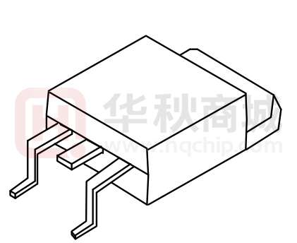
TO-252
P-channel
Absolute Maximum Ratings
Symbol
VDS
VGS
ID@TC=25℃
ID@TC=100℃
ID@TA=25℃
ID@TA=70℃
Parameter
Rating
Units
Drain-Source Voltage
-60
V
Gate-Source Voltage
±20
V
Continuous Drain Current, VGS @ -10V
1
-50
A
Continuous Drain Current, VGS @ -10V
1
-28
A
Continuous Drain Current, VGS @ -10V
1
-24.3
A
Continuous Drain Current, VGS @ -10V
1
-23.5
A
2
IDM
Pulsed Drain Current
EAS
Single Pulse Avalanche Energy
3
IAS
Avalanche Current
PD@TC=25℃
Total Power Dissipation
PD@TA=25℃
Total Power Dissipation
4
TSTG
TJ
-80
A
115
mJ
-45
A
4
52
W
2
W
Storage Temperature Range
-55 to 150
℃
Operating Junction Temperature Range
-55 to 150
℃
Thermal Data
Symbol
Typ.
Parameter
RθJA
Thermal Resistance Junction-Ambient
RθJC
1
NOV 2018 Version1.0
Thermal Resistance Junction-Case
1/7
1
Max.
Unit
---
62
℃/W
---
3.6
℃/W
www.ascendsemi.com
0755-86970486
�ASDM60P50KQ
-60V P-Channel MOSFET
Electrical Characteristics (TJ=25 ℃, unless otherwise noted)
Symbol
BVDSS
Parameter
Conditions
Drain-Source Breakdown Voltage
△BVDSS/△TJ BVDSS Temperature Coefficient
RDS(ON)
Static Drain-Source On-Resistance
VGS(th)
Gate Threshold Voltage
△VGS(th)
VGS(th) Temperature Coefficient
IDSS
Drain-Source Leakage Current
IGSS
2
Min.
Typ.
VGS=0V , ID=-250uA
-60
Reference to 25℃ , ID=-1mA
VGS=-10V , ID=-1A
VGS=-4.5V , ID=-1
VGS=VDS , ID =-250uA
Max.
Unit
-70
---
V
---
-0.03
---
V/℃
---
20
25
---
25
33
-1.0
-1.7-
m
-3.0
V
---
4.56
---
mV/℃
VDS=-60V , VGS=0V , TJ=25℃
---
---
1
uA
Gate-Source Leakage Current
VGS=±20V , VDS=0V
---
---
±100
nA
gfs
Forward Transconductance
VDS=-5V , ID=-12A
---
15.4
---
S
Rg
Gate Resistance
VDS=0V , VGS=0V , f=1MHz
Total Gate Charge (-4.5V)
Gate-Source Charge
13.5
26
-----
Qg
Qgs
-----
VDS=-48V , VGS=-4.5V , ID=-10A
---
3.08
---
Qgd
Gate-Drain Charge
---
2.95
---
Td(on)
Turn-On Delay Time
nC
---
28.8
---
Rise Time
VDD=-15V , VGS=-10V , RG=3.3,
---
19.8
---
Turn-Off Delay Time
ID=-1A
---
60.8
---
Fall Time
---
7.2
---
Ciss
Input Capacitance
---
3447
---
Coss
Output Capacitance
---
223
---
Crss
Reverse Transfer Capacitance
---
140
---
Min.
Typ.
Max.
Unit
---
---
-18
A
---
---
-36
A
---
---
-1.2
V
Tr
Td(off)
Tf
VDS=-15V , VGS=0V , f=1MHz
ns
pF
Diode Characteristics
Symbol
Parameter
IS
Continuous Source Current
ISM
Pulsed Source Current
VSD
2,5
Diode Forward Voltage
2
Conditions
1,5
VG=VD=0V , Force Current
VGS=0V , IS=-1A , TJ=25℃
Note :
1.The data tested by surface mounted on a 1 inch2 FR-4 board with 2OZ copper.
2.The data tested by pulsed , pulse width ≦ 300us , duty cycle ≦ 2%
3.The EAS data shows Max. rating . The test condition is VDD=-25V,VGS=-10V,L=0.1mH,IAS=-25.1A
4.The power dissipation is limited by 150℃ junction temperature
5.The data is theoretically the same as ID and IDM , in real applications , should be limited by total power dissipation.
NOV 2018 Version1.0
2/7
www.ascendsemi.com
0755-86970486
�ASDM60P50KQ
-60V P-Channel MOSFET
Typical Characteristics
160
12
ID=-12A
VGS=-3V
120
8
RDSON (mΩ)
-ID Drain Current (A)
10
6
VGS=-10V
4
80
VGS=-7V
VGS=-5V
2
VGS=-4.5V
0
40
0
0.5
1
1.5
-VDS , Drain-to-Source Voltage (V)
2
2
4
Fig.1 Typical Output Characteristics
6
-VGS (V)
8
10
Fig.2 On-Resistance v.s Gate-Source
12
10
ID=-12A
-VGS Gate to Source Voltage (V)
-IS Source Current(A)
10
8
6
TJ=150℃
TJ=25℃
4
2
0
0.2
0.4
0.6
0.8
8
6
4
2
0
0
1
-VSD , Source-to-Drain Voltage (V)
10
15
20
25
QG , Total Gate Charge (nC)
Fig.4 Gate-Charge Characteristics
Fig.3 Forward Characteristics of Reverse
2.5
Normalized On Resistance
1.5
Normalized VGS(th) (V)
5
2.0
1
1.5
0.5
1.0
0.5
0
-50
0
50
o 100
TJ ,Junction Temperature ( C)
Fig.5 Normalized VGS(th) v.s TJ
NOV 2018 Version1.0
3/7
150
-50
0
50
100
150
TJ , Junction Temperature (℃)
Fig.6 Normalized RDSON v.s TJ
www.ascendsemi.com
0755-86970486
�ASDM60P50KQ
-60V P-Channel MOSFET
100.00
10000
F=1.0MHz
10us
100us
Capacitance (pF)
Ciss
10.00
1ms
1000
-ID (A)
10ms
100ms
1.00
DC
Coss
100
0.10
Crss
TC=25℃
Single Pulse
0.01
10
1
5
9
13
17
-VDS Drain to Source Voltage(V)
21
25
0.1
1
10
100
1000
-VDS (V)
Fig.7 Capacitance
Fig.8 Safe Operating Area
Normalized Thermal Response (RθJC)
1
DUTY=0.5
0.2
0.1
0.1
0.05
0.02
0.01
P DM
0.01
T ON
T
SINGLE
D = TON/T
TJpeak = TC+P DMXRθJC
0.001
0.00001
0.0001
0.001
0.01
0.1
1
10
100
t , Pulse Width (s)
Fig.9 Normalized Maximum Transient Thermal Impedance
Fig.10 Switching Time Waveform
NOV 2018 Version1.0
4/7
Fig.11 Unclamped Inductive Waveform
www.ascendsemi.com
0755-86970486
�ASDM60P50KQ
-60V P-Channel MOSFET
Ordering and Marking Information
Device
Marking
Package
Packaging
Quantity
ASDM60P50KQ
60P50
TO-252
Tape&Reel
2500/Reel
MARKING
PACKAGE
Lot Number
TO-252
60P50
Date Code
NOV 2018 Version1.0
5/7
www.ascendsemi.com
0755-86970486
�ASDM60P50KQ
-60V P-Channel MOSFET
6\PERO
'LPHQVLRQV�LQ�0LOOLPHWHUV
'LPHQVLRQV�LQ�,QFKHV
0LQ
0D[
0LQ
0D[
$
����
����
�����
�����
$�
����
����
�����
�����
$�
����
����
�����
�����
E
����
����
�����
�����
E�
����
����
�����
�����
F
����
����
�����
�����
F�
����
����
�����
�����
'
����
����
�����
�����
'�
����
����
�����
�����
(
����
����
�����
�����
(�
����
����
�����
�����
+
����
����
�����
�����7
很抱歉,暂时无法提供与“ASDM60P50KQ-R”相匹配的价格&库存,您可以联系我们找货
免费人工找货- 国内价格
- 1+1.75500
- 100+1.63800
- 300+1.52100
- 500+1.40400
- 2000+1.34550
- 5000+1.31040


 工商网监
湘ICP备2023018690号
工商网监
湘ICP备2023018690号
