ASDM40N60KQ
40V N-Channel MOSFET
Product Summary
General Features
● High density cell design for ultra low Rdson
● Fully characterized avalanche voltage and current
● Good stability and uniformity with high EAS
● Excellent package for good heat dissipation
● Special process technology for high ESD capability
V DS
40
V
R DS(on),Typ@ VGS =10 V
7.0
mΩ
ID
60
A
Application
● Load switching
● Hard switched and high frequency circuits
● Uninterruptible power supply
TO-252-2L top view
Schematic diagram
Absolute Maximum Ratings (TC=25℃unless otherwise noted)
Symbol
Limit
Unit
Drain-Source Voltage
Parameter
VDS
40
V
Gate-Source Voltage
VGS
±20
V
ID
60
A
ID (100℃)
42
A
Pulsed Drain Current
IDM
240
A
Maximum Power Dissipation
PD
65
W
0.43
W/℃
EAS
400
mJ
TJ,TSTG
-55 To 175
℃
Drain Current-Continuous
Drain Current-Continuous(TC=100℃)
Derating factor
Single pulse avalanche energy
(Note 5)
Operating Junction and Storage Temperature Range
Thermal Characteristic
Thermal Resistance,Junction-to-Ambient
(Note 2)
Thermal Resistance,Junction-to-Case
NOV 2018 Version2.0
1/8
RθJA
62
℃/W
RθJC
2.8
℃/W
www.ascendsemi.com
0755-86970486
�ASDM40N60KQ
40V N-Channel MOSFET
Electrical Characteristics (TC=25℃unless otherwise noted)
Parameter
Symbol
Condition
Min
Typ
Max
Unit
Drain-Source Breakdown Voltage
BVDSS
VGS=0V ID=250μA
40
-
-
V
Zero Gate Voltage Drain Current
IDSS
VDS=40V,VGS=0V
-
-
1
μA
Gate-Body Leakage Current
IGSS
VGS=±20V,VDS=0V
-
-
±100
nA
Gate Threshold Voltage
VGS(th)
VDS=VGS,ID=250μA
1.2
1.6
2.5
V
Drain-Source On-State Resistance
RDS(ON)
VGS=10V, ID=20A
-
7.0
7.5
mΩ
Drain-Source On-State Resistance
RDS(ON)
VGS=4.5V, ID=20A
-
10.5
12
mΩ
gFS
VDS=10V,ID=20A
15
-
-
S
-
1520
-
PF
-
236
-
PF
-
160
-
PF
-
6.4
-
nS
Off Characteristics
On Characteristics
(Note 3)
Forward Transconductance
Dynamic Characteristics
(Note4)
Input Capacitance
Clss
Output Capacitance
Coss
Reverse Transfer Capacitance
Switching Characteristics
Crss
VDS=20V,VGS=0V,
F=1.0MHz
(Note 4)
Turn-on Delay Time
td(on)
Turn-on Rise Time
tr
VDD=20V,ID=2A,RL=1Ω
-
17.2
-
nS
td(off)
VGS=10V,RG=3Ω
-
29.6
-
nS
-
16.8
-
nS
-
29
nC
-
4.5
nC
-
6.4
nC
Turn-Off Delay Time
Turn-Off Fall Time
tf
Total Gate Charge
Qg
Gate-Source Charge
Qgs
Gate-Drain Charge
Qgd
VDS=20V,ID=20A,
VGS=10V
Drain-Source Diode Characteristics
Diode Forward Voltage
(Note 3)
VSD
Diode Forward Current
(Note 2)
IS
trr
Reverse Recovery Time
Reverse Recovery Charge
Qrr
Forward Turn-On Time
ton
VGS=0V,IS=10A
-
1.2
V
-
-
60
A
TJ = 25°C, IF = 20A
-
29
-
nS
(Note3)
-
26
-
nC
di/dt = 100A/μs
Intrinsic turn-on time is negligible (turn-on is dominated by LS+LD)
Notes:
1. Repetitive Rating: Pulse width limited by maximum junction temperature.
2. Surface Mounted on FR4 Board, t ≤ 10 sec.
3. Pulse Test: Pulse Width ≤ 300μs, Duty Cycle ≤ 2%.
4. Guaranteed by design, not subject to production
5. EAS condition : Tj=25℃,VDD=20V,VG=10V,L=1mH,Rg=25Ω,
NOV 2018 Version2.0
2/8
www.ascendsemi.com
0755-86970486
�ASDM40N60KQ
40V N-Channel MOSFET
ID- Drain Current (A)
Normalized On-Resistance
Typical Electrical and Thermal Characteristics (Curves)
TJ-Junction Temperature(℃)
Vds Drain-Source Voltage (V)
Figure 4 Rdson-JunctionTemperature
ID- Drain Current (A)
Vgs Gate-Source Voltage (V)
Figure 1 Output Characteristics
Qg Gate Charge (nC)
Figure 2 Transfer Characteristics
Figure 5 Gate Charge
Is- Reverse Drain Current (A)
Rdson On-Resistance(mΩ)
Vgs Gate-Source Voltage (V)
ID- Drain Current (A)
Figure 3 Rdson- Drain Current
NOV 2018 Version2.0
3/8
Vsd Source-Drain Voltage (V)
Figure 6 Source- Drain Diode Forward
www.ascendsemi.com
0755-86970486
�ASDM40N60KQ
C Capacitance (pF)
Power Dissipation (W)
40V N-Channel MOSFET
TJ-Junction Temperature (℃)
Figure 7 Capacitance vs Vds
Figure 9 Power De-rating
ID- Drain Current (A)
Vds Drain-Source Voltage (V)
TJ-Junction Temperature(℃)
Figure 8 Safe Operation Area
Figure 10 VGS(th) vs Junction Temperature
r(t),Normalized Effective
Transient Thermal Impedance
Vds Drain-Source Voltage (V)
Square Wave Pluse Duration(sec)
Figure 11 Normalized Maximum Transient Thermal Impedance
NOV 2018 Version2.0
4/8
www.ascendsemi.com
0755-86970486
�ASDM40N60KQ
40V N-Channel MOSFET
Test circuit
1) EAS Test Circuit
2) Gate Charge Test Circuit
3) Switch Time Test Circuit
NOV 2018 Version2.0
5/8
www.ascendsemi.com
0755-86970486
�ASDM40N60KQ
40V N-Channel MOSFET
Ordering and Marking Information
Ordering Device No.
Marking
Package
Packing
Quantity
ASDM40N60KQ-R
40N60
TO-252
Tape&Reel
2500/Reel
MARKING
PACKAGE
40N60
TO-252
NOV 2018 Version2.0
6/8
www.ascendsemi.com
0755-86970486
�ASDM40N60KQ
40V N-Channel MOSFET
TO-252 Package Information
Symbol
Dimensions In Millimeters
Dimensions In Inches
Min.
Max.
Min.
Max.
A
2.200
2.400
0.087
0.094
A1
0.000
0.127
0.000
0.005
b
0.660
0.860
0.026
0.034
c
0.460
0.580
0.018
0.023
D
6.500
6.700
0.256
0.264
D1
5.100
5.460
0.201
0.215
D2
4.830 TYP.
0.190 TYP.
E
6.000
6.200
0.236
0.244
e
2.186
2.386
0.086
0.094
L
9.800
10.400
0.386
0.409
L1
L2
2.900 TYP.
1.400
L3
0.114 TYP.
1.700
0.055
1.600 TYP.
0.067
0.063 TYP.
L4
0.600
1.000
0.024
0.039
Φ
1.100
1.300
0.043
0.051
θ
0°
8°
0°
8°
h
0.000
0.300
0.000
0.012
V
NOV 2018 Version2.0
5.350 TYP.
7/8
0.211 TYP.
www.ascendsemi.com
0755-86970486
�ASDM40N60KQ
40V N-Channel MOSFET
IMPORTANT NOTICE
ShenZhen Ascend Semiconductor incorporated MAKES NO WARRANTY OF ANY KIND, EXPRESS OR IMPLIED, WITH REGARDS TO THIS
DOCUMENT, INCLUDING, BUT NOT LIMITED TO, THE IMPLIED WARRANTIES OF MERCHANTABILITY AND FITNESS FOR A PARTICULAR
PURPOSE (AND THEIR EQUIVALENTS UNDER THE LAWS OF ANY JURISDICTION).
ShenZhen Ascend Semiconductor Incorporated and its subsidiaries reserve the right to make modifications, enhancements, improvements,
corrections or other changes without further notice to this document and any product described herein. ShenZhen Ascend Semiconductor
Incorporated does not assume any liability arising out of the application or use of this document or any product described herein; neither
does ShenZhen Ascend Semiconductor Incorporated convey any license under its patent or trademark rights, nor the rights of others. Any
Customer or user of this document or products described herein in such applications shall assume .
all risks of such use and will agree to hold Ascendsemi Incorporated and all the companies whose products are represented on ShenZhen
Ascend Semiconductor Incorporated website, harmless against all damages.
ShenZhen Ascend Semiconductor Incorporated does not warrant or accept any liability whatsoever in respect of any products purchased
through unauthorized sales channel. Should Customers purchase or use ShenZhen Ascend Semiconductor Incorporated products for any
unintended or unauthorized application, Customers shall indemnify and hold ShenZhen Ascend Semiconductor Incorporated and its
representatives harmless against all claims, damages, expenses, and attorney fees arising out of, directly or indirectly, any claim of personal
injury or death associated with such unintended or unauthorized application.
www.ascendsemi.com
NOV 2018 Version2.0
8/8
www.ascendsemi.com
0755-86970486
�
很抱歉,暂时无法提供与“ASDM40N60KQ-R”相匹配的价格&库存,您可以联系我们找货
免费人工找货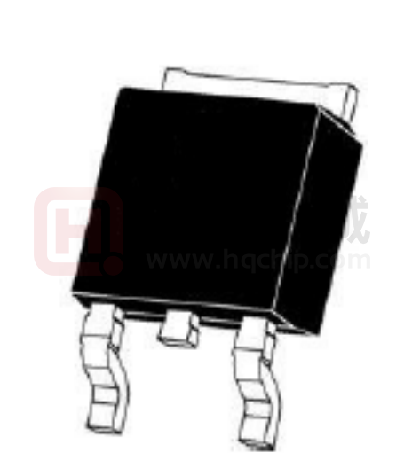


 工商网监
湘ICP备2023018690号
工商网监
湘ICP备2023018690号

