XC6206
300mA Low Power LDO
Features
Low power consumption
Low Quiescent Current: 5uA at 6V
Low voltage drop
Output voltage accuracy: tolerance ±2%
Low temperature coefficient
Applications
Battery-powered equipment
Portable AV systems
Reference voltage sources
Mobile phones
Cameras, video cameras
Portable games
General Description
XC6206 series are a highly precise, lower
compatible with low ESR ceramic capacitors. The
consumption,
voltage
current limiter’s foldback circuit operates as a
regulators manufactured using CMOS and laser
short circuit protection as well as the output
trimming technologies. The series provides large
current limiter for the output pin. Output voltages
currents with a significantly small
are internally by laser trimming technologies. It is
3
terminal,
positive
dropout
voltage .
selectable in 0.1V increments within a range of
The XC6206 consists of a current limiter circuit, a
3.0V to 3.6V. XC6206 series are available in
driver transistor, a precision reference voltage
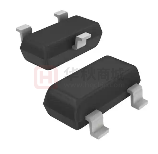
SOT-23 package.
and an error correction circuit. The series is
Order Information
XC6206-①②③④
Designator Symbol
Integer
①②
N
③
④
R
G
Description
Output Voltage(3.0~3.6V)
Package:SOT23
RoHS / Pb Free
Halogen Free
Note:”①②” stands for output voltages. Other voltages can be specially customized
Block Diagram
V1.0
1
Apr 18,2018
�XC6206
300mA Low Power LDO
Pin Assignment
SOT23 (Top View)
Table1: XC6206 series (SOT23 PKG)
PIN NO.
PIN NAME
FUNCTION
1
GND
GND pin
2
VOUT
Output voltage pin
3
VIN
Input voltage pin
Typical Application
Vo ut
Vin
VIN
+
C1
1 uF
VOUT
+
GND
C2
1 uF
XC6206
GND
GND
Marking Rule
① represents product number
MARK
6
PRODUCT SERIES
XC6206
② represents 3 pins regulator
MARK
VOLTAGE=0.1~3.0V VOLTAGE=3.1V~6.0V
5
6
V1.0
2
PRODUCT
SERIES
XC6206
Apr 18,2018
�XC6206
300mA Low Power LDO
③ represents output voltage
MARK
VOLTAGE(V)
0
3.1
1
3.2
2
3.3
3
3.4
4
3.5
5
3.6
6
3.7
7
3.8
8
3.9
9
4.0
A
4.1
B
1.2
4.2
C
1.3
4.3
D
1.4
4.4
E
1.5
4.5
MARK
F
H
K
L
M
N
P
R
S
T
U
V
X
Y
Z
-
VOLTAGE(V)
4.6
4.7
4.8
4.9
5.0
-
1.6
1.7
1.8
1.9
2.0
2.1
2.2
2.3
2.4
2.5
2.6
2.7
2.8
2.9
3.0
-
④ Z
Absolute Maximum Ratings
Parameter
Symbol
Ratings
Units
Input Voltage
VIN
8
V
Output Current
IOUT
300
mA
Output Voltage
VOUT
VSS-0.3~VIN+0.3
V
SOT-23
0.20
W
SOT23-3
0.25
W
0.50
W
USP-6B
0.10
W
TO-92
0.50
W
Power
Dissipation
Pd
SOT-89
*
Operating Temperature Range
Topr
-40~+85
℃
Storage Temperature Range
Tstg
-55~+125
℃
*IOUT=Pd/(VIN-VOUT)
V1.0
3
Apr 18,2018
�XC6206
300mA Low Power LDO
Electrical Characteristics
XC6206 for any output voltage
(Ta=25℃)
Parameter
Symbol
Output Voltage
Vout
Output Current*1
Iout
Low dropout*2
Vdrop
Line Regulation
Load Regulation
Conditions
Min.
Vin=Vout+1V
Vout×0.9
1.0mA≤Iout≤30mA
8
Vin-Vout=1V
--
-300
Max.
Unit
Vout×1.0
V
2
--
mA
Refer to the next table
1.6V≤Vin≤8V
△Vout1/(Vin·Vout
Iout=40mA
)
△Vout /ΔIout
Vin= Vout+1V
1.0mA≤Iout≤80mA
Output voltage
Temperature
Typ.
△Vout/(Ta·Vout)
Coefficiency
Iout=30mA
0℃≤Ta≤70℃
--
0.05
0.2
%/V
--
12
30
mV
--
±100
--
Ppm/℃
Supply Current
Iss
--
--
5
8
uA
Input Voltage
Vin
--
--
6
8
V
PSRR
PSRR
--
50
--
dB
Output Noise
EN
--
30
--
uVrms
F=1KHz
Vin=Vout+1V
BW=10Hz~
100KHz
Electrical Characteristics by Output Voltage:
Dropout Voltage Vdif(V)
Output Voltage
Vout(V)
Conditions
Vout≤1.5V
1.8 ≤ Vout ≤ 2
Iout=100 mA
2.8 ≤ Vout ≤ 5.0
V1.0
4
Typ.
Max.
0.50
0.68
0.39
0.53
0.28
0.39
Apr 18,2018
�XC6206
300mA Low Power LDO
Package Information
3-pin SOT23 Outline Dimensions
V1.0
5
Apr 18,2018
�
很抱歉,暂时无法提供与“XC6206-2.5NR”相匹配的价格&库存,您可以联系我们找货
免费人工找货- 国内价格
- 5+0.18232
- 20+0.16623
- 100+0.15015
- 500+0.13406
- 1000+0.12655
- 2000+0.12119


 工商网监
湘ICP备2023018690号
工商网监
湘ICP备2023018690号
