SY6885B
60V, 5A Full Protection Switch
General Description
Features
The SY6885B is a current limit switch with
programmable input over voltage protection and output
voltage clamping. Extremely low RDS(ON) of the
integrated protection N-channel FET helps to reduce
power loss during normal operation. Programmable
soft-start time controls the slew rate of the output
voltage during start-up. Independent enable control
allows the complicated system sequencing control. The
device also integrates thermal shutdown protection.
This device along with small QFN3×3-16 footprint
provides small PCB area application.
• Wide Input Voltage Range from 4V to 48V with
Surge up to 60V
• Low Bias Current: 100µA Typical
• Extremely Low RDS(ON) for the Integrated
Protection Switch: 40mΩ
• Programmable Soft-start
• Programmable Current Limit
• OCP/TSD/OVP Protection: Auto-recovery
• Input Over Voltage Protection with Adjustable
Threshold and Auto-recovery
• Programmable Output Voltage Clamping
• RoHS Compliant and Halogen Free
• Compact Package: QFN3×3-16
Ordering Information
SY6885 □(□□)□
Package type
QFN3×3-16
l-F
or
半
Typical Applications
• Notebook PC
• Server
• Service PC
Note
----
导
小
Ordering Number
SY6885BQDC
Applications
芯
Temperature Code
Package Code
Optional Spec Code
OUT
yC
Sil
erg
SY6885B Rev.0.9B
© 2021 Silergy Corp.
C8
(Opt.)
R3
OVP
SY6885B
R4
EN
C2
C3
VCP
R2
on
fid
VOUT
IN
R1
en
C5
C4
tia
VIN
D1
ILMT
GND
SS
C7
R5
Figure 1. Schematic Diagram
Silergy Corp. Confidential- Prepared for Customer Use Only
1
All Rights Reserved.
�SY6885B
VCP
GND
ILMT
SS
OVP
EN
Pinout (top view)
1
2
3
4
5
6
IN
7
8
IN
OUT
9
10
OUT
IN
11
12
IN
OUT
13
14
OUT
IN
15
16
IN
(QFN3×3-16)
Top Mark: BEOxyz (device code: BEO, x=year code, y=week code, z= lot number code)
Pin Number
IN
7,8,11,12,15,16
GND
2
OVP
5
ILMT
3
SS
4
EN
6
VCP
1
OUT
9, 10, 13, 14
Pin Description
Power input pin. Decouple high frequency noise by connecting at least 0.1µF
MLCC to ground.
Ground pin.
Over voltage protection input. Connect to the center of resistor divider. The
protection voltage is: VOVP = 1.2V× (R1+R2)/R2.
Current limit program pin. Connect a resistor from this pin to ground to program
the current limit.
Soft-start time program pin. Connect a capacitor to ground to program the softstart time.
Enable control input. Pull it high to enable the IC.
Output clamping voltage setting pin. The clamping voltage equals to
VCLAMP=1.2V× (R3+R4)/R4.
Power output pin.
Sil
erg
yC
on
fid
en
tia
l-F
or
半
导
小
芯
Pin Name
SY6885B Rev.0.9B
© 2021 Silergy Corp.
Silergy Corp. Confidential- Prepared for Customer Use Only
2
All Rights Reserved.
�SY6885B
Block Diagram
OUT
IN
Soft-start
SS
UVLO
Charge
Pump
Driver
Discharge
Control
EN
Current
Sense
ILMT
Control Logic
1.2Vref
OVP
VCP
1.2Vref
GND
Thermal
Detect
0.2Vref
芯
Figure 2. Block Diagram
导
小
Absolute Maximum Ratings (Note 1)
半
IN -------------------------------------- ---------------------------------------------------------- -0.3V to 60V
EN, OUT, OVP, VCP ---------------------------------------------------------------------------------------------- -0.3V to 60V
SS, ILMT ------------------------------------------------------------------------------------------------------------- -0.3V to 3.6V
Power Dissipation, PD @ TA = 25°C QFN3×3-16, -------------------------------------------------------------------- 2.463W
Package Thermal Resistance (Note 2)
l-F
or
θ JA ------------------------------------------------------------------------------------------------------------ 40.596°C/W
θ JC ------------------------------------------------------------------------------------------------------------ 10.656°C/W
fid
en
tia
Junction Temperature Range ------------------------------------------------------------------------------------- -40°C to 125°C
Lead Temperature (Soldering, 10 sec.) ------------------------------------------------------------------------------------ 260°C
Storage Temperature Range -------------------------------------------------------------------------------------- -65°C to 150°C
on
Recommended Operating Conditions (Note 3)
Sil
erg
yC
IN --------------------------------------------------------------------------------------------------------------------------- 4V to 48V
EN, OUT, OVP, VCP --------------------------------------------------------------------------------------------------- 0V to 48V
SS, ILMT ----------------------------------------------------------------------------------------------------------------- 0V to 3.3V
Junction Temperature Range ------------------------------------------------------------------------------------- -40°C to 125°C
SY6885B Rev.0.9B
© 2021 Silergy Corp.
Silergy Corp. Confidential- Prepared for Customer Use Only
3
All Rights Reserved.
�SY6885B
Electrical Characteristics
(VIN = 48V, CSST=100nF, CIN = 10µF, COUT = 10µF, TA = 25°C, unless otherwise specified)
Symbol
VIN
VUVLO
VHYS
IBIAS
ISHDN
RDS(ON)
ILMT
VVCPREF
VOVPREF
tOVP
VOVP,HYS
tSS
Test Conditions
VIN=48V, EN=3V
VIN=48V, EN=0
VIN=5V, EN=3V
(Note 5)
ILMT = 5A,VIN=5V
(Note 4)CSST=100nF,
VIN=24V, R3/R4=200k/10k
VEN_ON
VEN_OFF
RDIS
THYS
Typ
0.2
100
10
40
1
-30%
1.176
1.176
1.2
1.2
200
120
23.2
-30%
2
Max
48
3.9
150
60
5
30%
1.224
1.224
Unit
V
V
V
µA
µA
mΩ
A
ILIM
V
V
ns
mV
ms
30%
13k
V
V
Ω
150
°C
20
°C
0.4
芯
TSD
Min
4
3.5
导
小
Parameter
Input Voltage Range
Input UVLO Threshold
UVLO Hysteresis
Bias Current
Shutdown Current
Protection FET RON
Current Limit Program Range
Current Limit Accuracy
VCP Reference Voltage
OVP Reference Voltage
OVP Response Time
OVP Recovery Hysteresis
Soft-start Time
Soft-start Time Accuracy
EN Turn-on Threshold
EN Turn-off Threshold
Output Discharge Resistor
Thermal Shutdown
Temperature
Thermal Shutdown Hysteresis
l-F
or
半
Note 1: Stresses beyond the “Absolute Maximum Ratings” may cause permanent damage to the device. These are
stress ratings only. Functional operation of the device at these or any other conditions beyond those indicated in the
operational sections of the specification is not implied. Exposure to absolute maximum rating conditions for
extended periods may affect device reliability
en
tia
Note 2: θ JA is measured in the natural convection at TA = 25°C on a low effective single layer thermal conductivity
test board of JEDEC 51-3 thermal measurement standard. Pin1 of QFN3×3-16 packages is the case position for θ JC
measurement.
on
fid
Note 3: The device is not guaranteed to function outside its operating conditions.
yC
Note4: Recommended Current Soft-start Time Program Table
Sil
erg
SST cap (nF)
Rise (ms)
Condition: VIN=24V, R3/R4=200k/10k
None
10
47
1.4
2.8
13.1
100
27.8
Recommended formula for CSS & soft-start slew rate calculation:
R + R LOW
1
UP
, No external C7
T
R LOW
dv SS_DLT
voltage loop soft-start.
=
dt I INT R UP + R LOW
,t SS t SS_DLT
C7
R LOW
SY6885B Rev.0.9B
© 2021 Silergy Corp.
Silergy Corp. Confidential- Prepared for Customer Use Only
4
All Rights Reserved.
�SY6885B
1
1
, No external C7
T
R
di SS_DLT
ILMT 11
current loop soft-start.
=
dt I INT
1
,t t SS_DLT
C7 R ILMT 11 SST
Where, TSS_DLT is the internally fixed default soft-start time, about 1.4ms, which means there’s no any external C7;
IINT is the internal current source, about 4.1µA ; RUP and RLOW are the external resistors for output voltage OVP or
Clamping setting; RILMT is current limit setting resistor.
Note5: Recommended Current Limit Program Table
Current Limit Resistance (kΩ)
11
5.5
4.4
Current Limit (A)
1.0
2.0
2.5
Recommended Formula for RLIM & Current Limit Calculation:
3.1
3.5
2.8
4.0
2.4
4.5
2.2
5.0
11K
()
ILIM
Sil
erg
yC
on
fid
en
tia
l-F
or
半
导
小
芯
R5 =
3.7
3.0
SY6885B Rev.0.9B
© 2021 Silergy Corp.
Silergy Corp. Confidential- Prepared for Customer Use Only
5
All Rights Reserved.
�SY6885B
导
小
Bottom View
Sil
erg
yC
on
fid
en
tia
l-F
or
半
Top View
芯
QFN3×3-16 Package Outline Drawing
Side View
Notes:
Recommended PCB layout
(Reference Only)
All dimension in millimeter and exclude mold flash & metal burr.
SY6885B Rev.0.9B
© 2021 Silergy Corp.
Silergy Corp. Confidential- Prepared for Customer Use Only
6
All Rights Reserved.
�SY6885B
Taping & Reel Specification
1. Taping orientation
QFN3×3
导
小
芯
Feeding direction
Reel
Size
Sil
erg
yC
on
fid
en
tia
l-F
or
半
2. Carrier Tape & Reel specification for packages
Package
type
QFN3×3
Tape width
(mm)
Pocket
pitch(mm)
Reel size
(Inch)
Trailer
length(mm)
Leader length
(mm)
Qty per reel
(pcs)
12
8
13"
400
400
5000
3. Others: NA
SY6885B Rev.0.9B
© 2021 Silergy Corp.
Powered by TCPDF (www.tcpdf.org)
Silergy Corp. Confidential- Prepared for Customer Use Only
7
All Rights Reserved.
�
很抱歉,暂时无法提供与“SY6885BQDC”相匹配的价格&库存,您可以联系我们找货
免费人工找货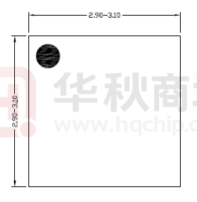


 工商网监
湘ICP备2023018690号
工商网监
湘ICP备2023018690号
