SS015N06LS
N-MOSFET 60V, 340A, 1.3mΩ
Description
SS015N06LS, the N-channel Enhanced Power
MOSFETs, is obtained by advanced double trench
technology which reduce the conduction loss,
improve switching performance and enhance the
avalanche energy. This is suitable device for motor
drivers and high speed switching applications.
Schematic Diagram
KEY CHARACTERISTICS
Parameter
Value
Unit
VDSS
60
V
ID
340
A
R DS(on).typ
1.3
mΩ
FEATURES:
Fast Switching
Low On-Resistance ( RDS(on)≤1.5mΩ )
Low Gate Charge
Low Reverse transfer capacitances
High avalanche ruggedness
RoHS product
APPLICATIONS:
Switching applications
Motor drivers
BMS
Synchronous rectification
ORDERING INFORMATION
Ordering Codes
Package
Product Code
SS015N06LS
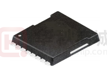
TOLL-8
SS015N06LS
WWW.SKYSEMI.COM
第1/10
Packing
Reel
深圳市思开半导体有限公司
�SS015N06LS
N-MOSFET 60V, 340A, 1.3mΩ
2. ABSOLUTE RATINGS
at TC=25°C,unless otherwise specified
Symbol
Parameter
Drain-Source Voltage
V DSS
ID
IDM
Note1
V GS
E AS Note2
PD
T J ,T stg
TL
Rating
Units
60
V
Continuous Drain Current, Silicon Limited
370
A
Continuous Drain Current, Package Limited
340
A
Continuous Drain Current @T C =100°C, Silicon Limited
265
A
Pulsed Drain Current
1200
A
Gate-Source Voltage
±20
V
Avalanche Energy
1450
mJ
Power Dissipation
410
W
Derating Factor above 25°C
2.85
W/ ℃
175 ,–55 to 175
℃
260
℃
Operating Junction and Storage Temperature Range
Maximum Temperature for Soldering
Note1: Repetitive Rating: Pulse width limited by maximum junction temperature
Note2: L=0.5mH, Ias=77A Start TJ =25℃
3. Thermal characteristics
Symbol
Parameter
Max
R θJC
R θJA
thermal resistance, Junction-Case
0.37
℃/W
40
℃/W
4.
thermal resistance, Junction-Ambient
Units
Electrical Characteristics
at TC=25°C, unless otherwise specified
OFF Characteristics
Symbol
V DSS
Parameter
Drain-Source
Voltage
Breakdown
Values
Test Conditions
Min
Typ
Max
Units
V GS =0V, I=250µA
60
--
--
V
V DS =60V, V G S =0V
--
--
1
µA
V DS =50, V G S =0V
@T C =125°C
--
--
100
µA
IDSS
Drain-Source Leakage Current
IGSS(F)
Gate-Source Forward Leakage
V GS =+20V
--
--
100
nA
IGSS(R)
Gate-Source Reverse Leakage
V GS =-20V
--
--
-100
nA
WWW.SKYSEMI.COM
第2/10
深圳市思开半导体有限公司
�SS015N06LS
N-MOSFET 60V, 340A, 1.3mΩ
ON Characteristics
Symbol
Parameter
Values
Test Conditions
Drain-Source On-Resistance
R DS(on)
Gate Threshold Voltage
V GS(th)
Pulse width tp ≤300µs, δ≤2%
Min
V GS =10V, I D =50A
V DS =V G S , I D =250µA
Dynamic Characteristics
Typ
Max
--
1.3
1.5
mΩ
2.0
3.0
4.0
V
Values
Typ
Symbol Parameter
Test Conditions
Ciss
Coss
Crss
Qg
Qgs
Qgd
Input Capacitance
VDS=30V,
7373
Output Capacitance
VGS=0,
4297
Reverse Transfer Capacitance
f=1MHz
139
Total Gate Charge
VDD=30V,
165
Gate-Source charge
ID=50A,
42
Gate-Drain charge
VGS=10V
51
Min
Units
Max
Units
pF
nC
Switching Characteristics
Symbol
Parameter
Symbol
td(on)
tr
td(off)
tf
Parameter
Turn-On Delay
Values
Test Conditions
Time
Rise Time
Test Conditions
VDD=30V,
ID=50A,
VGS=10V,
RG=3Ω,
Resistive Load
Turn-Off Delay Time
Fall Time
Min
Typ
Max
--
32
--
--
96
--
--
78
--
--
102
--
Units
Units
ns
Source-Drain Diode Characteristics
Symbol
Parameter
Test Conditions
ISymbol
S
I SM
V SD
T rr
Q rr
Parameter
Continuous
Source Current
Conditions
TTest
C=25°C
(Package limit)
Maximum Pulsed Current
Values
Units
Typ
Max
--
--
340
Units
A
TC=25°C,tplimited by Tjmax
--
--
1200
A
Diode Forward Voltage
V GS =0V, I S =50A
--
--
1.4
V
Reverse Recovery Time
If=50A,VGS=0,
--
103
--
ns
Reverse Recovery Charge
di/dt=100A/us
--
298
--
nC
WWW.SKYSEMI.COM
第3/10
Min
深圳市思开半导体有限公司
�SS015N06LS
N-MOSFET 60V, 340A, 1.3mΩ
5. Characteristics Curves
Figure 2. Maximum Power Dissipation vs Case
Figure 1. Safe Operating Area
Temperature
Figure 3. Maximum Continuous Drain Current
vs Case Temperature
WWW.SKYSEMI.COM
第4/10
Figure 4. Typical Output Characteristics
深圳市思开半导体有限公司
�SS015N06LS
N-MOSFET 60V, 340A, 1.3mΩ
Figure 5. Transient Thermal Impedance
Figure 6. Typical Transfer Characteristics
WWW.SKYSEMI.COM
第5/10
Figure 7. Source-Drain Diode Forward
Characteristics
深圳市思开半导体有限公司
�SS015N06LS
N-MOSFET 60V, 340A, 1.3mΩ
Figure 8. Drain-Source On-Resistance vs
Figure 9. Normalized On-Resistance vs
Drain Current
Junction Temperature
Figure 10. Normalized Threshold Voltage vs
Figure 11. Normalized Breakdown Voltage vs
Junction Temperature
Junction Temperature
WWW.SKYSEMI.COM
第6/10
深圳市思开半导体有限公司
�SS015N06LS
N-MOSFET 60V, 340A, 1.3mΩ
Figure 13. Typical Gate Charge vs
Figure 12. Capacitance Characteristics
WWW.SKYSEMI.COM
Gate-Source Voltage
第7/10
深圳市思开半导体有限公司
�SS015N06LS
N-MOSFET 60V, 340A, 1.3mΩ
6. Test Circuit and Waveform
WWW.SKYSEMI.COM
第8/10
深圳市思开半导体有限公司
�SS015N06LS
N-MOSFET 60V, 340A, 1.3mΩ
WWW.SKYSEMI.COM
第9/10
深圳市思开半导体有限公司
�SS015N06LS
N-MOSFET 60V, 340A, 1.3mΩ
7. Package Description TOLL-8
WWW.SKYSEMI.COM
第10/10
深圳市思开半导体有限公司
�


 工商网监
湘ICP备2023018690号
工商网监
湘ICP备2023018690号
