RF64
ADVANCED COMMUNICATIONS
& SENSING300-510MHz Transceiver
Ultra-Low
Power Integrated
General Description
Features
The RF64 is a low cost single-chip transceiver
operating in the frequency ranges from 300MHz to
510MHz. The RF64 is optimized for very low power
consumption (3mA in receiver mode). It incorporates a
baseband modem with data rates up to 150 kb/s. Data
handling features include a sixty-four byte FIFO,
packet handling, automatic CRC generation and data
whitening. Its highly integrated architecture allows for
minimum external component count whilst maintaining
design flexibility. All major RF communication
parameters are programmable and most of them may
be dynamically set. It complies with European (ETSI
EN 300-220 V2.1.1) and North American (FCC part
15.247 and 15.249) regulatory standards.
Ordering Information
Low Rx power consumption: 3mA
Low Tx power consumption: 25 mA @ +10 dBm
Good reception sensitivity: down to -104 dBm at
25 kb/s in FSK, -110 dBm at 2kb/s in OOK
Programmable RF output power: up to +12.5 dBm
in 8 steps
Packet handling feature with data whitening and
automatic CRC generation
RSSI (Received Signal Strength Indicator)
Bit rates up to 150 kb/s, NRZ coding
On-chip frequency synthesizer
FSK and OOK modulation
Incoming sync word recognition
Built-in Bit-Synchronizer for incoming data and
clock synchronization and recovery
5 x 5 mm TQFN package
Optimized Circuit Configuration for Low-cost
applications
Table 1: Ordering Information
Part number
RF64
Delivery
Minimum Order
Quantity / Multiple
Tape & Reel
3000 pieces
TQFN-32 package – Operating range [-40;+85°C]
Trefers to Lead Free packaging
This device is WEEE and RoHS compliant
Applications
Wireless alarm and security systems
Wireless sensor networks
Automated Meter Reading
Home and building automation
Industrial monitoring and control
Remote Wireless Control
Active RFID PHY
Application Circuit Schematic
Page 1 of 76
Tel: +86-755-82973805 Fax: +86-755-82973550 E-mail: sales@hoperf.com http://www.hoperf.com
�RF64
ADVANCED COMMUNICATIONS & SENSING
Table of Contents
1. General Description ................................................................... 5
1.1. Simplified Block Diagram.................................................. 5
1.2. Pin Diagram ....................................................................... 6
1.3. Pin Description...................................................................7
2. Electrical Characteristics............................................................8
2.1. ESD Notice ........................................................................ 8
2.2. Absolute Maximum Ratings ............................................... .8
2.3. Operating Range ............................................................... 8
2.4. Chip Specification ............................................................... 8
2.4.1. Power Consumption ................................................... 8
2.4.2. Frequency Synthesis................................................. 9
2.4.3. Transmitter ................................................................. 9
2.4.4. Receiver ................................................................... 10
2.4.5. Digital Specification .................................................. 11
3. Architecture Description ............................................................ 12
3.1. Power Supply Strategy ..................................................... 12
3.2. Frequency Synthesis Description .................................... .13
3.2.1. Reference Oscillator................................................ 13
3.2.2. CLKOUT Output ....................................................... 13
3.2.3. PLL Architecture...................................................... 14
3.2.4. PLL Tradeoffs.......................................................... 14
3.2.5. Voltage Controlled Oscillator................................... 15
3.2.6. PLL Loop Filter ......................................................... 16
3.2.7. PLL Lock Detection Indicator .................................. 16
3.2.8. Frequency Calculation ............................................ 16
3.3. Transmitter Description ................................................... 18
3.3.1. Architecture Description ........................................... 18
3.3.2. Bit Rate Setting ....................................................... 19
3.3.3. Alternative Settings ................................................. 19
3.3.4. Fdev Setting in FSK Mode ...................................... 19
3.3.5. Fdev Setting in OOK Mode ..................................... 19
3.3.6. Interpolation Filter ................................................... 20
3.3.7. Power Amplifier ........................................................ 20
3.3.8. Common Input and Output Front-End ...................... 22
3.4. Receiver Description........................................................ 23
3.4.1. Architecture ............................................................. 23
3.4.2. LNA and First Mixer ................................................ 24
3.4.3. IF Gain and Second I/Q Mixer................................. 24
3.4.4. Channel Filters ........................................................ 24
3.4.5. Channel Filters Setting in FSK Mode ...................... .25
3.4.6. Channel Filters Setting in OOK Mode ..................... .26
3.4.7. RSSI ........................................................................ 26
3.4.8. Fdev Setting in Receive Mode ................................ 28
3.4.9. FSK Demodulator.................................................... 28
3.4.10. OOK Demodulator................................................. 28
3.4.11. Bit Synchronizer ..................................................... 31
3.4.12. Alternative Settings ............................................... 32
3.4.13. Data Output ............................................................ 32
4. Operating Modes...................................................................... 33
4.1. Modes of Operation .......................................................... 33
4.2. Digital Pin Configuration vs. Chip Mode ........................... 33
5. Data Processing....................................................................... 34
5.1. Overview.......................................................................... 34
5.1.1. Block Diagram .......................................................... 34
5.1.2. Data Operation Modes ............................................. 34
5.2. Control Block Description ................................................. 35
5.2.1. SPI Interface ........................................................... 35
5.2.2. FIFO ......................................................................... 38
5.2.3. Sync Word Recognition........................................... 39
5.2.4. Packet Handler........................................................ 40
5.2.5. Control......................................................................40
5.3. Continuous Mode .............................................................41
5.3.1. General Description .................................................41
5.3.2. Tx Processing ..........................................................41
5.3.3. Rx Processing ...........................................................42
5.3.4. Interrupt Signals Mapping .........................................42
5.3.5. uC Connections........................................................43
5.3.6. Continuous Mode Example .......................................43
5.4. Buffered Mode ..................................................................44
5.4.1. General Description .................................................44
5.4.2. Tx Processing ..........................................................44
5.4.3. Rx Processing ...........................................................45
5.4.4. Interrupt Signals Mapping .........................................46
5.4.5. uC Connections........................................................47
5.4.6. Buffered Mode Example...........................................47
5.5. Packet Mode.....................................................................49
5.5.1. General Description .................................................49
5.5.2. Packet Format ..........................................................49
5.5.3. Tx Processing ..........................................................51
5.5.4. Rx Processing ...........................................................51
5.5.5. Packet Filtering ........................................................52
5.5.6. DC-Free Data Mechanisms......................................53
5.5.7. Interrupt Signal Mapping ...........................................54
5.5.8. uC Connections........................................................55
5.5.9. Packet Mode Example .............................................56
5.5.10. Additional Information ............................................56
6. Configuration and Status Registers ..........................................58
6.1. General Description ...........................................................58
6.2. Main Configuration Register - MCParam..........................58
6.3. Interrupt Configuration Parameters - IRQParam ................60
6.4. Receiver Configuration parameters - RXParam .................62
6.5. Sync Word Parameters - SYNCParam.............................63
6.6. Transmitter Parameters - TXParam .................................64
6.7. Oscillator Parameters - OSCParam .................................64
6.8. Packet Handling Parameters – PKTParam .......................65
7. Application Information .............................................................66
7.1. Crystal Resonator Specification .......................................66
7.2. Software for Frequency Calculation .................................66
7.2.1. GUI ...........................................................................66
7.2.2. .dll for Automatic Production Bench ..........................66
7.3. Switching Times and Procedures ......................................66
7.3.1. Optimized Receive Cycle .........................................67
7.3.2. Optimized Transmit Cycle ........................................68
7.3.3. Transmitter Frequency Hop Optimized Cycle ..........69
7.3.4. Receiver Frequency Hop Optimized Cycle ..............70
7.3.5. Rx=>Tx and Tx=>Rx Jump Cycles ............................71
7.4. Reset of the Chip ...............................................................72
7.4.1. POR .........................................................................72
7.4.2. Manual Reset ............................................................72
7.5. Reference Design ..............................................................73
7.5.1. Application Schematic ...............................................73
7.5.2. PCB Layout ...............................................................73
7.5.3. Bill Of Material ...........................................................74
8. Packaging Information ...............................................................75
8.1. Package Outline Drawing ..................................................75
8.2. PCB Land Pattern.............................................................75
9. Contact Information...................................................................76
Page 2 of 76
Tel: +86-755-82973805 Fax: +86-755-82973550 E-mail: sales@hoperf.com http://www.hoperf.com
�RF64
ADVANCED COMMUNICATIONS & SENSING
Index of Figures
Figure 1: RF64 Simplified Block Diagram ....................................... 5
Figure 2: RF64 Pin Diagram .......................................................... 6
Figure 3: RF64 Detailed Block Diagram ...................................... 12
Figure 4: Power Supply Breakdown............................................. 13
Figure 5: Frequency Synthesizer Description ............................... 14
Figure 6: LO Generator ................................................................ 14
Figure 7: Loop Filter ..................................................................... 16
Figure 8: Transmitter Architecture ............................................... 18
Figure 9: I(t), Q(t) Overview ......................................................... 18
Figure 10: PA Control................................................................... 21
Figure 11: Optimal Load Impedance Chart ................................... 21
Figure 12: Recommended PA Biasing and Output Matching ..... 22
Figure 13: Front-end Description ................................................. 22
Figure 14: Receiver Architecture ................................................. 23
Figure 15: FSK Receiver Setting ................................................. 23
Figure 16: OOK Receiver Setting ................................................ 23
Figure 17: Active Channel Filter Description................................ 24
Figure 18: Butterworth Filter's Actual BW .................................... 26
Figure 19: Polyphase Filter's Actual BW ...................................... 26
Figure 20: RSSI Dynamic Range ................................................. 27
Figure 21: RSSI IRQ Timings ...................................................... 28
Figure 22: OOK Demodulator Description .................................... 29
Figure 23: Floor Threshold Optimization...................................... 30
Figure 24: BitSync Description..................................................... 31
Figure 25: RF64‟s Data Processing Conceptual View .................. 34
Figure 26: SPI Interface Overview and uC Connections ............. 35
Figure 27: Write Register Sequence ............................................. 36
Figure 28: Read Register Sequence............................................ 37
Figure 29: Write Bytes Sequence (ex: 2 bytes) ........................... 37
Figure 30: Read Bytes Sequence (ex: 2 bytes) ........................... 38
Figure 31: FIFO and Shift Register (SR)...................................... 38
Figure 32: FIFO Threshold IRQ Source Behavior........................ 39
Figure 33: Sync Word Recognition ...............................................40
Figure 34: Continuous Mode Conceptual View.............................41
Figure 35: Tx Processing in Continuous Mode .............................41
Figure 36: Rx Processing in Continuous Mode.............................42
Figure 37: uC Connections in Continuous Mode ..........................43
Figure 38: Buffered Mode Conceptual View .................................44
Figure 39: Tx processing in Buffered Mode (FIFO size = 16,
Tx_start_irq_0=0) ..............................................................45
Figure 40: Rx Processing in Buffered Mode (FIFO size=16,
Fifo_fill_method=0)............................................................46
Figure 41: uC Connections in Buffered Mode ................................47
Figure 42: Packet Mode Conceptual View .....................................49
Figure 43: Fixed Length Packet Format........................................50
Figure 44: Variable Length Packet Format ....................................51
Figure 45: CRC Implementation ...................................................53
Figure 46: Manchester Encoding/Decoding ...................................54
Figure 47: Data Whitening .............................................................54
Figure 48: uC Connections in Packet Mode .................................55
Figure 49: Optimized Rx Cycle .....................................................67
Figure 50: Optimized Tx Cycle......................................................68
Figure 51: Tx Hop Cycle ...............................................................69
Figure 52: Rx Hop Cycle ...............................................................70
Figure 53: Rx => Tx => Rx Cycle ..................................................71
Figure 54: POR Timing Diagram...................................................72
Figure 55: Manual Reset Timing Diagram ....................................72
Figure 56: Reference Design Circuit Schematic ............................73
Figure 57: Reference Design„s Stackup .......................................74
Figure 58: Reference Design Layout (top view)............................74
Figure 59: Package Outline Drawing .............................................75
Figure 60: PCB Land Pattern .........................................................75
Page 3 of 76
Tel: +86-755-82973805 Fax: +86-755-82973550 E-mail: sales@hoperf.com http://www.hoperf.com
�RF64
ADVANCED COMMUNICATIONS & SENSING
Index of Tables
Table 1: Ordering Information ......................................................... 1
Table 2: RF64 Pinouts ................................................................... 7
Table 3: Absolute Maximum Ratings ............................................. 8
Table 4: Operating Range.............................................................. 8
Table 5: Power Consumption Specification .................................... 8
Table 6: Frequency Synthesizer Specification ................................ 9
Table 7: Transmitter Specification ................................................. 9
Table 8: Receiver Specification.................................................... 10
Table 9: Digital Specification........................................................ 11
Table 10: MCParam_Freq_band Setting ..................................... 15
Table 11: PA Rise/Fall Times....................................................... 20
Table 12: Operating Modes ......................................................... 33
Table 13: Pin Configuration vs. Chip Mode ................................. 33
Table 14: Data Operation Mode Selection .................................... 35
Table 15: Config vs. Data SPI Interface Selection ........................ 36
Table 16: Status of FIFO when Switching Between Different
Modes of the Chip ............................................................. 39
Table 17: Interrupt Mapping in Continuous Rx Mode .................. 42
Table 18: Interrupt Mapping in Continuous Tx Mode .................... 42
Table 19: Relevant Configuration Registers in Continuous Mode
(data processing related only) ............................................43
Table 20: Interrupt Mapping in Buffered Rx and Stby Modes ........46
Table 21: Interrupt Mapping in Tx Buffered Mode ........................46
Table 22: Relevant Configuration Registers in Buffered Mode (data
processing related only) .....................................................47
Table 23: Interrupt Mapping in Rx and Stby in Packet Mode........55
Table 24: Interrupt Mapping in Tx Packet Mode ............................55
Table 25: Relevant Configuration Registers in Packet Mode (data
processing related only) .....................................................56
Table 26: Registers List ................................................................58
Table 27: MCParam Register Description ....................................58
Table 28: IRQParam Register Description....................................60
Table 29: RXParam Register Description ......................................62
Table 30: SYNCParam Register Description .................................63
Table 31: TXParam Register Description .....................................64
Table 32: OSCParam Register Description ...................................64
Table 33: PKTParam Register Description ....................................65
Table 34: Crystal Resonator Specification .....................................66
Table 35: Reference Design BOM .................................................74
Acronyms
Page 4 of 76
Tel: +86-755-82973805 Fax: +86-755-82973550 E-mail: sales@hoperf.com http://www.hoperf.com
�RF64
ADVANCED COMMUNICATIONS & SENSING
This product datasheet contains a detailed description of the RF64 performance and functionality.
1. General Description
The RF64 is a single chip FSK and OOK transceiver capable of operation in the 300 to 510MHz license free ISM
frequency bands. It complies with both the relevant European and North American standards, EN 300-220 V2.1.1
(June 2006 release) and FCC Part 15 (10-1-2006 edition). A unique feature of this circuit is its extremely low
current consumption in receiver mode of only 3mA (typ).
The RF64 comes in a 5x5 mm TQFN-32 package.
1.1. Simplified Block Diagram
Figure 1: RF64 Simplified Block Diagram
Page 5 of 76
Tel: +86-755-82973805 Fax: +86-755-82973550 E-mail: sales@hoperf.com http://www.hoperf.com
�RF64
ADVANCED COMMUNICATIONS & SENSING
1.2. Pin Diagram
The following diagram shows the pins arrangement of the QFN package, top view.
Figure 2: RF64 Pin Diagram
Notes:
yyww refers to the date
code
------ refers to the lot
number
Page 6 of 76
Tel: +86-755-82973805 Fax: +86-755-82973550 E-mail: sales@hoperf.com http://www.hoperf.com
�RF64
ADVANCED COMMUNICATIONS & SENSING
1.3. Pin Description
Table 2: RF64 Pinouts
Number
0
1
2
3
4
5
6
7
8
9
10
11
12
13
14
15
16
17
18
19
20
21
22
23
24
25
26
27
28
Name
GND
TEST5
TEST1
VR_VCO
VCO_M
VCO_P
LF_M
LF_P
TEST6
TEST7
XTAL_P
XTAL_M
TEST0
TEST8
NSS_CONFIG
NSS_DATA
MISO
MOSI
SCK
CLKOUT
DATA
IRQ_0
IRQ_1
PLL_LOCK
TEST2
TEST3
VDD
VR_1V
VR_DIG
Type
I
I/O
I/O
O
I/O
I/O
I/O
I/O
I/O
I/O
I/O
I/O
I
I/O
I
I
O
I
I
O
I/O
O
O
O
O
I/O
I
O
O
29
30
31
32
VR_PA
TEST4
NC
RFIO
O
I/O
I/O
Description
Exposed ground pad
Connect to GND
Connect to GND
Regulated supply of the VCO
VCO tank
VCO tank
PLL loop filter
PLL loop filter
Connect to GND
Connect to GND
Crystal connection
Crystal connection
Connect to GND
POR. Do not connect if unused
SPI CONFIG enable
SPI DATA enable
SPI data output
SPI data input
SPI clock input
Clock output
NRZ data input and output (Continuous mode)
Interrupt output
Interrupt output
PLL lock detection output
No connect
Connect to GND
Supply voltage
Regulated supply of the analog circuitry
Regulated supply of digital circuitry
Regulated supply of the PA
Connect to GND
Connect to GND
RF input/output
Note: pin 13 (Test 8) can be used as a manual reset trigger. See section 7.4.2 for details on its use.
Page 7 of 76
Tel: +86-755-82973805 Fax: +86-755-82973550 E-mail: sales@hoperf.com http://www.hoperf.com
�RF64
ADVANCED COMMUNICATIONS & SENSING
2. Electrical Characteristics
2.1. ESD Notice
The RF64 is a high performance radio frequency device. It satisfies:
Class 2 of the JEDEC standard JESD22-A114-B (Human Body Model), except on pins 3-4-5-27-28-2932 where it satisfies Class 1A.
Class III of the JEDEC standard JESD22-C101C (Charged Device Model) on all pins. It should thus be handled with
all the necessary ESD precautions to avoid any permanent damage.
2.2. Absolute Maximum Ratings
Stresses above the values listed below may cause permanent device failure. Exposure to absolute maximum
ratings for extended periods may affect device reliability.
Table 3: Absolute Maximum Ratings
Symbol
VDDmr
Tmr
Pmr
Description
Supply voltage
Storage temperature
Input level
Min
-0.3
-55
-
Max
3.7
125
0
Min
2.1
-40
-
Max
3.6
+85
0
Unit
V
°C
dBm
2.3. Operating Range
Table 4: Operating Range
Symbol
VDDop
Trop
ML
Description
Supply Voltage
Temperature
Input Level
Unit
V
°C
dBm
2.4. Chip Specification
Conditions: Temp = 25 °C, VDD = 3.3 V, crystal frequency = 12.8 MHz, carrier frequency = 434 MHz, modulation
FSK, data rate = 25 kb/s, Fdev = 50 kHz, fc = 100 kHz, unless otherwise specified.
2.4.1. Power Consumption
Table 5: Power Consumption Specification
Symbol
IDDSL
IDDST
IDDFS
IDDR
IDDT
(1)
Description
Supply current in sleep
mode
Supply current in standby
mode, CLKOUT disabled
Supply current in FS mode
Supply current in receiver
mode
Supply current in
transmitter mode
Conditions
Min
Typ
Max
-
0.1
2
µA
Crystal oscillator running
-
65
85
µA
Frequency synthesizer
running
-
1.3
1.7
mA
-
3.0
3.5
mA
-
25
16
30
21
mA
mA
Output power = +10 dBm
(1)
Output power = 1dBm
Unit
Guaranteed by design and characterization
Page 8 of 76
Tel: +86-755-82973805 Fax: +86-755-82973550 E-mail: sales@hoperf.com http://www.hoperf.com
�RF64
ADVANCED COMMUNICATIONS & SENSING
2.4.2. Frequency Synthesis
Table 6: Frequency Synthesizer Specification
Symbol
Description
Conditions
FR
Frequency ranges
Programmable ,
(may require specific BOM)
BR_F
BR_O
FDA
XTAL
Bit rate (FSK)
Bit rate (OOK)
Frequency deviation (FSK)
Crystal oscillator frequency
Frequency synthesizer
step
Oscillator wake-up time
Frequency synthesizer
wake-up time at most
10 kHz away from the
target
FSTEP
TS_OSC
TS_FS
Frequency synthesizer hop
time at most 10 kHz away
from the target
TS_HOP
(1)
Min
300
320
350
390
430
470
0.78
0.78
33
9
Typ
50
12.8
Max
330
350
390
430
470
510
150
32
200
15
Unit
MHz
MHz
MHz
MHz
MHz
MHz
Kb/s
Kb/s
kHz
MHz
-
2
-
kHz
-
1.5
5
ms
From Stby mode
-
500
800
µs
200 kHz step
1 MHz step
-
180
200
-
µs
µs
5 MHz step
-
250
-
µs
7 MHz step
-
260
-
µs
12 MHz step
-
290
-
µs
20 MHz step
-
320
-
µs
27 MHz step
-
340
-
µs
Min
Typ
Max
Unit
NRZ
NRZ
Variable, depending on the
frequency.
(1)
From Sleep mode
Guaranteed by design and characterization
2.4.3. Transmitter
Table 7: Transmitter Specification
Symbol
Description
Conditions
Maximum power setting
-
+12.5
-
dBm
RFOP
RF output power,
programmable with 8 steps
of typ. 3dB
Minimum power setting
-
-8.5
-
dBm
-
-112
-
dBc/Hz
-
-
-47
dBc
PN
Phase noise
SPT
Transmitted spurious
(1)
TS_TR
TS_TR2
(1)
(1)
Measured with a 600 kHz
offset, at the transmitter
output.
At any offset between
200 kHz and 600 kHz,
unmodulated carrier, Fdev
= 50 kHz.
Transmitter wake-up time
From FS to Tx ready.
-
120
500
µs
Transmitter wake-up time
From Stby to Tx ready.
-
600
900
µs
Guaranteed by design and characterization
Page 9 of 76
Tel: +86-755-82973805 Fax: +86-755-82973550 E-mail: sales@hoperf.com http://www.hoperf.com
�RF64
ADVANCED COMMUNICATIONS & SENSING
2.4.4. Receiver
On the following table, fc and fo describe the bandwidth of the active channel filters as described in section 3.4.4.2.
All sensitivities are measured receiving a PN15 sequence, for a BER of 0.1.%
Table 8: Receiver Specification
Symbol
Description
RFS_F
Conditions
434 MHz, BR=25 kb/s, Fdev
=50 kHz, fc=100 kHz
Sensitivity (FSK)
434 MHz, 2kb/s NRZ
fc-fo=50 kHz, fo=50 kHz
RFS_O
Sensitivity (OOK)
CCR
Co-channel rejection
ACR
Adjacent channel
rejection
BI
Blocking immunity
RXBW_F
(1,2)
(1,2)
RXBW_O
IIP3
(1)
TS_RE
(1)
TS_RE2
Receiver bandwidth in
FSK mode
Receiver bandwidth in
OOK mode
Input 3rd order intercept
point
Receiver wake-up time
Receiver wake-up time
TS_RE_HOP
Receiver hop time from
Rx ready to Rx ready with
a frequency hop
TS_RSSI
DR_RSSI
RSSI sampling time
RSSI dynamic Range
(1)
(2)
Modulation as wanted signal
Offset = 300 kHz
Offset = 600 kHz
Offset = 1.2 MHz
Offset = 1 MHz,
unmodulated
Offset = 2 MHz,
unmodulated, no SAW
Offset = 10 MHz,
unmodulated, no SAW
Single side BW
Polyphase Off
Single side BW
Polyphase On
Interferers at 1MHz and
1.950 MHz offset
From FS to Rx ready
From Stby to Rx ready
200 kHz step
1MHz step
5MHz step
7MHz step
12MHz step
20MHz step
27MHz step
From Rx ready
Ranging from sensitivity
Min
Typ
Max
Unit
-
-104
-
dBm
-
-
-
-
-110
-
dBm
-
-12
42
53
-
dBc
dB
dB
dB
-
53
-
dBc
-
-
-
-
-
-
50
-
250
kHz
50
-
400
kHz
-
-28
-
dBm
-
280
600
400
400
460
480
520
550
600
70
500
900
1/Fdev
-
µs
µs
µs
µs
µs
µs
µs
µs
µs
s
dB
Information from design and characterization
This reflects the whole receiver bandwidth, as described in sections 3.4.4.1 and 3.4.4.2
Page 10 of 76
Tel: +86-755-82973805 Fax: +86-755-82973550 E-mail: sales@hoperf.com http://www.hoperf.com
�RF64
ADVANCED COMMUNICATIONS & SENSING
2.4.5. Digital Specification
Conditions: Temp = 25 °C, VDD = 3.3 V, crystal frequency = 12.8 MHz, unless otherwise specified.
Table 9: Digital Specification
Symbol
VIH
VIL
VOH
VOL
SCK_CONFIG
SCK_DATA
T_DATA
T_MOSI_C
T_MOSI_D
T_NSSC_L
T_NSSD_L
T_NSSC_H
T_NSSD_H
Description
Digital input level high
Digital input level low
Digital output level high
Digital output level low
SPI Config. clock frequency
SPI data clock frequency
DATA hold and setup time
MOSI setup time for SPI Config.
MOSI setup time for SPI Data.
NSS_CONFIG low to SCK rising edge.
SCK falling edge to NSS_CONFIG high.
NSS_DATA low to SCK rising edge.
SCK falling edge to NSS_DATA high.
NSS_CONFIG rising to falling edge.
NSS_DATA rising to falling edge.
Conditions
Imax=1mA
Imax=-1mA
Min
0.8*VDD
0.9*VDD
2
250
312
Typ
-
Max
0.2*VDD
0.1*VDD
6
1
-
Unit
V
V
V
V
MHz
MHz
µs
ns
ns
500
-
-
ns
625
-
-
ns
500
625
-
-
ns
ns
Note: on pin 10 (XTAL_P) and 11 (XTAL_N), maximum voltages of 1.8V can be applied.
Page 11 of 76
Tel: +86-755-82973805 Fax: +86-755-82973550 E-mail: sales@hoperf.com http://www.hoperf.com
�RF64
ADVANCED COMMUNICATIONS & SENSING
3. Architecture Description
This section describes in depth the architecture of this ultra low-power transceiver:
VR_PA
PA
I
Q
LO2 Tx
I
Q
LO2 Tx
W aveform
generator
I
RFIO
LO1 Tx
Q
RSSI
OOK
demod
BitSync
LNA
Control
FSK
demod
LO2 Rx
IRQ_0
IRQ_1
MOSI
MISO
SCK
NSS_CONFIG
NSS_DATA
CLKOUT
DATA
L O 1 Rx
TEST
LO1 Rx
PLL_LOCK
I LO2 Rx
Q
XTAL_P
XO
Frequency Synthesizer
LO
Generator
XTAL_M
I LO1 Tx
Q
I LO2 Tx
Q
VR_1V
VR_DIG
VCO_P
VCO_M
VR_VCO
LF_M
LF_P
Figure 3: RF64 Detailed Block Diagram
3.1. Power Supply Strategy
To provide stable sensitivity and linearity characteristics over a wide supply range, the RF64 is internally
regulated. This internal regulated power supply structure is described below:
Page 12 of 76
Tel: +86-755-82973805 Fax: +86-755-82973550 E-mail: sales@hoperf.com http://www.hoperf.com
�RF64
ADVANCED COMMUNICATIONS & SENSING
1ųF
Y5V
Vbat
VDD – Pin 26
2.1 – 3.6V
External Supply
Reg_top
1.4 V
Biasing :
-SPI
-Config. Registers
-POR
Reg_dig
1.0 V
Biasing digital
blocks
Reg_VCO
0.85 V
Biasing :
-VCO circuit
-Ext. VCO
tank
Biasing analog
blocks
VR_VCO
Pin 3
VR_DIG
Pin 28
220nF
X7R
Reg_PA
1.80 V
100nF
X7R
Biasing :
-PA Driver
-PA choke
(ext)
VR_PA
Pin 29
VR_1V
Pin 27
1ųF
Y5V
47nF
X7R
Figure 4: Power Supply Breakdown
To ensure correct operation of the regulator circuit, the decoupling capacitor connection shown in Figure 4 is
required. These decoupling components are recommended for any design.
3.2. Frequency Synthesis Description
The frequency synthesizer of the RF64 is a fully integrated integer-N type PLL. The PLL circuit requires only five
external components for the PLL loop filter and the VCO tank circuit.
3.2.1. Reference Oscillator
The RF64 embeds a crystal oscillator, which provides the reference frequency for the PLL. The recommended
crystal specification is given in section 7.1.
3.2.2. CLKOUT Output
The reference frequency, or a sub-multiple of it, can be provided on CLKOUT (pin 19) by activating the bit
OSCParam_Clkout_on. The division ratio is programmed through bits OSCParam_Clkout_freq. The two
applications of the CLKOUT output are:
To provide a clock output for a companion uC, thus saving the cost of an additional oscillator. CLKOUT can be
made available in any operation mode, except Sleep mode, and is automatically enabled at power-up.
To provide an oscillator reference output. Measurement of the CLKOUT signal enables simple software
trimming of the initial crystal tolerance.
Note: To minimize the current consumption of the RF64, ensure that the CLKOUT signal is disabled when unused.
Page 13 of 76
Tel: +86-755-82973805 Fax: +86-755-82973550 E-mail: sales@hoperf.com http://www.hoperf.com
�RF64
ADVANCED COMMUNICATIONS & SENSING
3.2.3. PLL Architecture
The crystal oscillator (XO) forms the reference oscillator of an Integer-N Phase Locked Loop (PLL), whose
operation is discussed in the following section. Figure 5 shows a block schematic of the RF64 PLL. Here the crystal
reference frequency and the software controlled dividers R, P and S determine the output frequency of the PLL.
(P
÷75.
)+
i
S
i+1
LO
PFD
÷(Ri+1)
XO
XT_M
XT_P
Vtu e
n
Fcom p
LF_M
LF_P
VCO_P
VCO_M
VR_VCO
Figure 5: Frequency Synthesizer Description
The VCO tank inductors are connected on an external differential input. Similarly, the loop filter is also located
externally. However, there is an internal 8pF capacitance at VCO input that should be subtracted from the desired
loop filter capacitance.
The output signal of the VCO is used as the input to the local oscillator (LO) generator stage, illustrated in Figure 6.
The VCO frequency is subdivided and used in a series of up (down) conversions for transmission (reception).
LO1 Rx
Receiver
LOs
I
LO2 Rx
÷8
90°
Q
LO
VCO Output
I
LO1 Tx
90°
Q
Transmitter
LOs
I
LO2 Tx
÷8
90°
Q
Figure 6: LO Generator
3.2.4. PLL Tradeoffs
With an integer-N PLL architecture, the following criterion must be met to ensure correct operation:
The comparison frequency, Fcomp, of the Phase Frequency Detector (PFD) input must remain higher than six
times the PLL bandwidth (PLLBW) to guarantee loop stability and to reject harmonics of the comparison
frequency Fcomp. This is expressed in the inequality:
PLLBW ≤
Fcomp
6
However the PLLBW has to be sufficiently high to allow adequate PLL lock times
Because the divider ration R determines Fcomp, it should be set close to 119, leading to Fcomp≈100 kHz
which will ensure suitable PLL stability and speed.
Page 14 of 76
Tel: +86-755-82973805 Fax: +86-755-82973550 E-mail: sales@hoperf.com http://www.hoperf.com
�RF64
ADVANCED COMMUNICATIONS & SENSING
With the recommended Bill Of Materials (BOM) of the reference design of section 7.5.3, the PLL prototype is the
following:
64 ≤ R ≤ 169
S < P+1
LLBW = 15 kHz nominal
Startup times and reference frequency spurs as specified.
3.2.5. Voltage Controlled Oscillator
The integrated VCO requires only two external tank circuit inductors. As the input is differential, the two inductors
should have the same nominal value. The performance of these components is important for both the phase noise
and the power consumption of the PLL. It is recommended that a pair of high Q factor inductors is selected. These
should be mounted orthogonally to other inductors (in particular the PA choke) to reduce spurious coupling
between the PA and VCO. In addition, such measures may reduce radiated pulling effects and undesirable
transient behavior, thus minimizing spectral occupancy. Note that ensuring a symmetrical layout of the VCO
inductors will further improve PLL spectral purity.
For best performance wound type inductors, with tight tolerance, should be used as described in section 7.5.3.
3.2.5.1. SW Settings of the VCO
To guarantee the optimum operation of the VCO over the RF64‟s frequency and temperature ranges, the
following settings should be programmed into the RF64:
Target channel
(MHz)
Freq_band
300330
000
320350
001
350390
010
390430
011
430470
100
470510
101
Table 10: MCParam_Freq_band Setting
3.2.5.2. Trimming the VCO Tank by Hardware and Software
To ensure that the frequency band of operation may be accurately addressed by the R, P and S dividers of the
synthesizer, it is necessary to ensure that the VCO is correctly centered. Note that for the reference design (see
section 7.5) no centering is necessary. However, any deviation from the reference design may require the
optimization procedure, outlined below, to be implemented. This procedure is simplified thanks to the built-in VCO
trimming feature which is controlled over the SPI interface. This tuning does not require any RF test equipment,
and can be achieved by simply measuring Vtune, the voltage between pins 6 (LFM) and 7 (LFP).
The VCO is centered if the voltage is within the range:
100 ≤ Vtune(mV ) ≤ 200
Note that this measurement should be conducted when in transmit mode at the center frequency of the desired
band (for example ~315 MHz in the 300-330 MHz band), with the appropriate MCParam_Freq_band setting.
If this inequality is not satisfied then adjust the MCParam_VCO_trim bits from 00 whilst monitoring Vtune. This
allows the VCO voltage to be trimmed in + 60 mV increments. Should the desired voltage range be inaccessible,
the voltage may be adjusted further by changing the tank circuit inductance value. Note that an increase in
inductance will result in an increase Vtune.
Page 15 of 76
Tel: +86-755-82973805 Fax: +86-755-82973550 E-mail: sales@hoperf.com http://www.hoperf.com
�RF64
ADVANCED COMMUNICATIONS & SENSING
Note for mass production: The VCO capacitance is piece to piece dependant. As such, the optimization proposed
above should be verified on several prototypes, to ensure that the population is centered on 150 mV.
3.2.6. PLL Loop Filter
To adequately reject spurious components arising from the comparison frequency Fcomp, an external 2
loop filter is employed.
nd
order
RL1
LF_M
CL2
CL1
LF_P
Figure 7: Loop Filter
Following the recommendations made in section 3.2.4, the loop filter proposed in the reference design‟s bill of
material on section 7.5.3 should be used. The loop filter settings are frequency band independent and are hence
relevant to all implementations of the RF64.
3.2.7. PLL Lock Detection Indicator
The RF64 also features a PLL lock detect indicator. This is useful for optimizing power consumption, by adjusting
the synthesizer wake up time (TS_FS), since the PLL startup time is lower than specified under nominal conditions.
The lock status can be read on bit IRQParam_PLL_lock, and must be cleared by writing a “1” to this same register.
In addition, the lock status can be reflected in pin 23 PLL_LOCK, by setting the bit IRQParam_Enable_lock_detect.
3.2.8. Frequency Calculation
As shown in Figure 5 the PLL structure comprises three different dividers, R, P and S, which set the output
frequency through the LO. A second set of dividers is also available to allow rapid switching between a pair of
frequencies: R1/P1/S1 and R2/P2/S2. These six dividers are programmed by six bytes of the register MCParam
from addresses 6 to 11.
3.2.8.1. FSK Mode
The following formula gives the relationship between the local oscillator, and R, P and S values, when using FSK
modulation.
9
Flo
8
9 Fxtal
Frf , fsk
75P 1) S
8 R 1
Frf , fsk
3.2.8.2. OOK Mode
Due to the manner in which the baseband OOK symbols are generated, the signal is always offset by the FSK
frequency deviation (Fdev - as programmed in MCParam_Freq_dev). Hence, the center of the transmitted OOK
signal is:
Page 16 of 76
Tel: +86-755-82973805 Fax: +86-755-82973550 E-mail: sales@hoperf.com http://www.hoperf.com
�RF64
ADVANCED COMMUNICATIONS & SENSING
Consequently, in receive mode, due to the low intermediate frequency (Low-IF) architecture of the RF64 the
frequency should be configured so as to ensure the correct low-IF receiver baseband center frequency, IF2.
Note that from Section 3.4.4, it is recommended that IF2 be set to 100 kHz.
Page 17 of 76
Tel: +86-755-82973805 Fax: +86-755-82973550 E-mail: sales@hoperf.com http://www.hoperf.com
�RF64
ADVANCED COMMUNICATIONS & SENSING
3.3. Transmitter Description
The RF64 is set to transmit mode when MCParam_Chip_mode = 100.
Am plificati on
Int erpolation
filters
First up-c onversion
Second
up- conv ersion
DACs
DDS
Data
W av eform
I
LO2 Tx
gene rator
Q
Clock
I
RFIO
LO1 Tx
PA
Q
I
LO2 Tx
Q
RF
Baseband
IF
Figure 8: Transmitter Architecture
3.3.1. Architecture Description
The baseband I and Q signals are digitally generated by a DDS whose digital to analog converters (DAC) followed
by two anti-aliasing low-pass filters transform the digital signal into analog in-phase (I) and quadrature (Q)
components whose frequency is the selected frequency deviation (Fdev).
1
Fdev
I(t)
Q(t)
Figure 9: I(t), Q(t) Overview
In FSK mode, the relative phase of I and Q is switched by the input data between -90°and +90°with continuous
phase. The modulation is therefore performed at this initial stage, since the information contained in the phase
difference will be converted into a frequency shift when the I and Q signals are up-converted in the first mixer
stage. This first up-conversion stage is duplicated to enhance image rejection. The FSK convention is such that:
DATA ' '1' ' Frf Fdev
DATA ' '0' ' Frf Fdev
Page 18 of 76
Tel: +86-755-82973805 Fax: +86-755-82973550 E-mail: sales@hoperf.com http://www.hoperf.com
�RF64
ADVANCED COMMUNICATIONS & SENSING
In OOK mode, the phase difference between the I and Q channels is kept constant (independent of the transmitted
data). Thus, the first stage of up-conversion creates a fixed frequency signal at the low IF = Fdev (This explains
why the transmitted OOK spectrum is offset by Fdev).
OOK Modulation is accomplished by switching on and off the PA and PA regulator stages. By convention:
After the interpolation filters, a set of four mixers combines the I and Q signals and converts them into a pair of
complex signals at the second intermediate frequency, equal to 1/8 of the LO frequency, or 1/9 of the RF
frequency. These two new I and Q signals are then combined and up-converted to the final RF frequency by two
quadrature mixers fed by the LO signal. The signal is pre-amplified, and then the transmitter output is driven by a
final power amplifier stage.
3.3.2. Bit Rate Setting
In Continuous transmit mode, setting the Bit Rate is useful to determine the frequency of DCLK. As explained in
section 5.3.2, DCLK will trigger an interrupt on the uC each time a new bit has to be transmitted.
3.3.3. Alternative Settings
Bit rate, frequency deviation and TX interpolation filter settings are a function of the reference oscillator crystal
frequency, FXTAL. Settings other than those programmable with a 12.8 MHz crystal can be obtained by selection of
the correct reference oscillator frequency.
3.3.4. Fdev Setting in FSK Mode
The frequency deviation, Fdev, of the FSK transmitter is programmed through bits MCParam_Freq_dev:
It should be noted that for communications between a pair of RF64s, that Fdev should be at least 33 kHz to ensure
a correct operation on the receiver side.
3.3.5. Fdev Setting in OOK Mode
Fdev has no physical meaning in OOK transmit mode. However, as has been shown - due to the DDS baseband
signal generation, the OOK signal is always offset by “-Fdev” (see formulas is section 3.2.8). It is suggested that
Fdev retains its default value of 100 kHz in OOK mode.
Page 19 of 76
Tel: +86-755-82973805 Fax: +86-755-82973550 E-mail: sales@hoperf.com http://www.hoperf.com
�RF64
ADVANCED COMMUNICATIONS & SENSING
3.3.6. Interpolation Filter
After digital to analog conversion, both I and Q signals are smoothed by interpolation filters. This block low-pass
filters the digitally generated signal, and prevents the alias signals from entering the modulators. Its bandwidth can
be programmed with the register RXParam_InterpFiltTx, and should be set to:
Where Fdev is the programmed frequency deviation as set in MCParam_Freq_dev, and BR is the physical Bit Rate
of transmission.
Notes:
Low interpolation filter bandwidth will attenuate the baseband I/Q signals thus reducing the power of the FSK
signal. Conversely, excessive bandwidth will degrade spectral purity.
For the wideband FSK modulation, for example when operating in DTS mode, the recommended filter setting
can not be reached. However, the impact upon spectral purity will be negligible, due to the already wideband
channel.
3.3.7. Power Amplifier
The Power Amplifier (PA) integrated in the RF64 operates under a regulated voltage supply of 1.8 V. The
external PA choke inductor is biased by an internal regulator output made available on pin 29 (VR_PA). Thanks to
these features, the PA output power is consistent over the power supply range. This is important for mobile
applications where this allows both predictable RF performance and battery life.
3.3.7.1. Rise and Fall Times Control
In OOK mode, the PA ramp times can be accurately controlled through the MCParam_PA_ramp register. Those
bits directly control the slew rate of VR_PA output (pin 29).
Table 11: PA Rise/Fall Times
MCParam_PA_ramp
00
01
10
11
tVR_PA
3 us
8.5 us
15 us
23 us
tPA_OUT (rise / fall)
2.5 / 2 us
5 / 3 us
10 / 6 us
20 / 10 us
Page 20 of 76
Tel: +86-755-82973805 Fax: +86-755-82973550 E-mail: sales@hoperf.com http://www.hoperf.com
�RF64
ADVANCED COMMUNICATIONS & SENSING
DATA
VR_PA
[V]
95 %
95 %
tVR_PA
PA Output
power
tVR_PA
60 dB
60 dB
tPA_OUT
tPA_OUT
Figure 10: PA Control
3.3.7.2. Optimum Load Impedance (value to confirm)
As the PA and the LNA front-ends in the RF64 share the same Input/Output pin, they are internally matched to
approximately 50 Ω.
Pmax-1dB circle
Max Power
Zopt = 30+j25 Ω
Figure 11: Optimal Load Impedance Chart
Please refer to the reference design section for an optimized PA load setting.
Page 21 of 76
Tel: +86-755-82973805 Fax: +86-755-82973550 E-mail: sales@hoperf.com http://www.hoperf.com
�RF64
ADVANCED COMMUNICATIONS & SENSING
3.3.7.3. Suggested PA Biasing and Matching
The recommended PA bias and matching circuit is illustrated below:
VR_PA
47nF
100nH
Antenna
port
SAW
PA
RFIO
DC block
Low-pass and DC block
Figure 12: Recommended PA Biasing and Output Matching
Please refer to section 7.5.3 of this document for the optimized matching arrangement for each frequency band.
3.3.8. Common Input and Output Front-End
The receiver and the transmitter share the same RFIO pin (pin 32). Figure 13 below shows the configuration of the
common RF front-end.
In transmit mode, the PA and the PA regulator are active, with the voltage on the VR_PA pin equal to the
nominal voltage of the regulator (1.8 V). The external inductance is used to bias the PA.
In receive mode, both PA and PA regulator are off and VR_PA is tied to ground. The external inductance LT1
is then used to bias the LNA.
VR_PA
R eg_PA
Rx _on
PA
To
RFIO
LNA
Figure 13: Front-end Description
Page 22 of 76
Tel: +86-755-82973805 Fax: +86-755-82973550 E-mail: sales@hoperf.com http://www.hoperf.com
�RF64
ADVANCED COMMUNICATIONS & SENSING
3.4. Receiver Description
The RF64 is set to receive mode when MCParam_Chip_mode = 011.
Second downconv ersion
Fi rst downconve rsion
RSSI
OOK
demod
Cont rol logi c
-Patte rn recognition
-FIFO handl er
-SPI int erface
-Packet handl er
Bi t
synchronizer
F SK
demod
LO2 Rx
LNA
LO1 Rx
Baseband, IF2 in OOK
IF1
RF
Figure 14: Receiver Architecture
3.4.1. Architecture
th
The RF64 receiver employs a super-heterodyne architecture. Here, the first IF is 1/9 of the RF frequency
(approximately 100MHz). The second down-conversion down-converts the I and Q signals to base band in the
case of the FSK receiver (Zero IF) and to a low-IF (IF2) for the OOK receiver.
Second
down-conversion
LO2
Rx
First
down-conversion
0
IF1
≈100MHz
IF2=0
in FSK
mode
Image
frequency
LO1 Rx
Channel
Image
frequency
LO1 Rx
Channel
Frequencyl
Figure 15: FSK Receiver Setting
First
down-conversion
Second
down-conversion
0
IF2 Continuous)
Defines IRQ_0 source in Rx mode
Enables Sync word recognition
Defines Sync word size
Defines the error tolerance on Sync word recognition
Defines Sync word value
Tx Mode:
Go to Tx mode (and wait for Tx to be ready, see Figure 50)
Send all packet‟s bits on DATA pin synchronously with DCLK signal provided on IRQ_1
Go to Sleep mode
Rx Mode:
Program Rx interrupts: IRQ_0 mapped to Sync (Rx_stby_irq_0=”00”) and IRQ_1 mapped to DCLK (Bit
synchronizer enabled)
Go to Rx mode (note that Rx is not ready immediately, see Figure 49)
Wait for Sync interrupt
Get all packet bits on DATA pin synchronously with DCLK signal provided on IRQ_1
Go to Sleep mode
Page 43 of 76
Tel: +86-755-82973805 Fax: +86-755-82973550 E-mail: sales@hoperf.com http://www.hoperf.com
�RF64
ADVANCED COMMUNICATIONS & SENSING
5.4. Buffered Mode
5.4.1. General Description
As illustrated in Figure 38, for Buffered mode operation the NRZ data to (from) the (de)modulator is not directly
accessed by the uC but stored in the FIFO and accessed via the SPI Data interface. This frees the uC for other
tasks between processing data from the RF64, furthermore it simplifies software development and reduces uC
performance requirements (speed, reactivity). Note that in this mode the packet handler stays inactive.
An important feature is also the ability to empty the FIFO in Stby mode, ensuring low power consumption and
adding greater software flexibility.
RF64
IRQ_0
CONTROL
IRQ_1
Data
Rx
SPI
SYNC
RECOG.
NSS_CONFIG
CONFIG
FIFO
(+SR)
Tx
DATA
NSS_DATA
SCK
MOSI
MISO
Datapath
Figure 38: Buffered Mode Conceptual View
Note that Bit Synchronizer is automatically enabled in Buffered mode.
activated by the user if needed.
The Sync word recognition must be
5.4.2. Tx Processing
After entering Tx in Buffered mode, the chip expects the uC to write into the FIFO, via the SPI Data interface, all the
data bytes to be transmitted (preamble, Sync word, payload...).
Actual transmission of first byte will start either when the FIFO is not empty (i.e. first byte written by the uC) or when
the FIFO is full depending on bit IRQParam_Tx_start_irq_0.
In Buffered mode the packet length is not limited, i.e. as long as there are bytes inside the FIFO they are sent.
When the last byte is transferred to the SR, /Fifoempty IRQ source is asserted to warn the uC, at that time FIFO
can still be filled with additional bytes if needed.
When the last bit of the last byte has left the SR (i.e. 8 bit periods later), the Tx_done interrupt source is asserted
and the user can exit Tx mode after waiting at least 1 bit period from the last bit processed by modulator.
Page 44 of 76
Tel: +86-755-82973805 Fax: +86-755-82973550 E-mail: sales@hoperf.com http://www.hoperf.com
�RF64
ADVANCED COMMUNICATIONS & SENSING
If the transmitter is switched off (for example due to entering another chip mode) during transmission it will stop
immediately, even if there is still unsent data.
Figure 39 illustrates Tx processing with a 16 byte FIFO depth and Tx_start_irq_0=0. Please note that in this
example the packet length is equal to FIFO size, but this does not need to be the case, the uC can use the FIFO
interrupts anytime during Tx to manage FIFO contents and write additional bytes.
Start condition
(Cf. Tx_start_irq_0)
Fifofull
/Fifoempty
Tx_done
from
SPI Data
15
FIFO
0
b15
b14
b13
b12
b11
b10
b9
b8
b7
b6
b5
b4
b3
b2
b1
b0
Data Tx
(from SR)
XXX
b0
b1
b2
b3
b4
b5
b6
b7
b8
b9
b10
b11
b12
b13
b14
b15
XXX
Figure 39: Tx processing in Buffered Mode (FIFO size = 16, Tx_start_irq_0=0)
5.4.3. Rx Processing
After entering Rx in Buffered mode, the chip requires the uC to retrieve the received data from the FIFO. The FIFO
will actually start being filled with received bytes either; when a Sync word has been detected (in this case only the
bytes following the Sync word are filled into the FIFO) or when the Fifo_fill bit is asserted by the user - depending
on the state of bit, IRQParam_Fifo_fill_method.
In Buffered mode, the packet length is not limited i.e. as long as Fifo_fill is set, the received bytes are shifted into
the FIFO.
The uC software must therefore manage the transfer of the FIFO contents by interrupt and ensure reception of the
correct number of bytes. (In this mode, even if the remote transmitter has stopped, the demodulator will output
random bits from noise)
When the FIFO is full, Fifofull IRQ source is asserted to alert the uC, that at that time, the FIFO can still be unfilled
without data loss. If the FIFO is not unfilled, once the SR is also full (i.e. 8 bits periods later) Fifo_overrun_clr is
asserted and SR‟s content is lost.
Figure 40 illustrates an Rx processing with a 16 bytes FIFO size and Fifo_fill_method=0. Please note that in the
illustrative example of section 5.4.6, the uC does not retrieve any byte from the FIFO through SPI Data, causing
overrun.
Page 45 of 76
Tel: +86-755-82973805 Fax: +86-755-82973550 E-mail: sales@hoperf.com http://www.hoperf.com
�RF64
ADVANCED COMMUNICATIONS & SENSING
Data Rx
(to SR) “noisy” data
Preamble
Sync
b0
b1
b2
b3
b4
b5
b6
b7
b8
b9
b10
b11
b12 b13
b14 b15
b16
Start condition
(Cf. Fifo_fill_method)
/Fifoempty
Fifofull
Fifo_overrun_clr
Write_byte
15
b9
FIFO
b4
0
b0
b1
b2
b5
b6
b7
b10
b11
b12
b13
b14
b15
b8
b3
Figure 40: Rx Processing in Buffered Mode (FIFO size=16, Fifo_fill_method=0)
5.4.4. Interrupt Signals Mapping
The tables below describe the interrupts available in Buffered mode.
IRQ_0
IRQ_1
Rx_stby_irq_x
00 (d)
01
10
11
00 (d)
01
10
11
Rx
Write_byte
/Fifoempty
Sync
Fifofull
RSSI
Fifo_threshold
Stby
/Fifoempty
Fifofull
Fifo_threshold
Table 20: Interrupt Mapping in Buffered Rx and Stby Modes
IRQ_0
IRQ_1
Tx_start_irq_0=0 (d)
Tx
Fifo_threshold
Tx_start_irq_0=1
/Fifoempty
Tx_irq_1=0 (d)
Fifofull
Tx_irq_1=1
Tx_done
Table 21: Interrupt Mapping in Tx Buffered Mode
Page 46 of 76
Tel: +86-755-82973805 Fax: +86-755-82973550 E-mail: sales@hoperf.com http://www.hoperf.com
�RF64
ADVANCED COMMUNICATIONS & SENSING
5.4.5. uC Connections
RF64
IRQ_0
IRQ_1
NSS_CONFIG
NSS_DATA
SCK
MOSI
MISO
uC
Figure 41: uC Connections in Buffered Mode
Note that depending upon the application, some uC connections may not be needed:
IRQ_0: if none of the relevant IRQ sources are used. In this case, leave floating.
IRQ_1: if none of the relevant IRQ sources are used. In this case, leave floating.
MISO: if no read register access is needed and the chip is used in Tx mode only. In this case, pull up to VDD
through a 100 kΩ resistor.
In addition, DATA pin (unused in buffered mode) should be pulled-up to VDD through a 100 kΩ resistor.
Please refer to Table 13 for the RF64‟s pin configuration.
5.4.6. Buffered Mode Example
Configure all data processing related registers listed below appropriately. In this example we assume Sync
word recognition is on and Fifo_fill_method=0.
MCParam
IRQParam
RXParam
SYNCParam
Data_mode_x
Fifo_size
Fifo_thresh
Rx_stby_irq_0
Rx_stby_irq_1
Tx_irq_1
Fifo_fill_method
Fifo_fill
Tx_start_irq_0
Sync_size
Sync_tol
Sync_value
Tx
X
X
X
Rx
X
X
X
X
X
X
X
X
X
X
X
X
Description
Defines data operation mode (=>Buffered)
Defines FIFO size
Defines FIFO threshold
Defines IRQ_0 source in Rx & Stby modes
Defines IRQ_1 source in Rx & Stby modes
Defines IRQ_1 source in Tx mode
Defines FIFO filling method
Controls FIFO filling status
Defines Tx start condition and IRQ_0 source
Defines Sync word size
Defines the error tolerance on Sync word detection
Defines Sync word value
Table 22: Relevant Configuration Registers in Buffered Mode (data processing related only)
Tx Mode:
Program Tx start condition and IRQs: Start Tx when FIFO is not empty (Tx_start_irq_0=1) and IRQ_1 mapped
to Tx_done (Tx_irq_1=1)
Go to Tx mode (and wait for Tx to be ready, see Figure 50)
Page 47 of 76
Tel: +86-755-82973805 Fax: +86-755-82973550 E-mail: sales@hoperf.com http://www.hoperf.com
�RF64
ADVANCED COMMUNICATIONS & SENSING
Write packet bytes into FIFO. Tx starts when the first byte is written (Tx_start_irq_0=1). We assume the FIFO is
being filled via SPI Data faster than being unfilled by SR (else use Tx_start_irq_0=0 ie Fifo_threshold to delay
Tx start)
Wait for Tx_done interrupt (+1 bit period)
Go to Sleep mode
Rx Mode:
Program Rx/Stby interrupts: IRQ_0 mapped to /Fifoempty (Rx_stby_irq_0=10) and IRQ_1 mapped to
Fifo_threshold (Rx_stby_irq_1=01). Configure Fifo_thresh to an appropriate value (ex: to detect packet end if
its length is known)
Go to Rx mode (note that Rx is not ready immediately, Cf section 7.3.1).
Wait for Fifo_threshold interrupt (i.e. Sync word has been detected and FIFO filled up to the defined threshold).
If it is packet end, go to Stby (SR‟s content is lost).
Read packet bytes from FIFO until /Fifoempty goes low (or correct number of bytes is read).
Go to Sleep mode.
Page 48 of 76
Tel: +86-755-82973805 Fax: +86-755-82973550 E-mail: sales@hoperf.com http://www.hoperf.com
�RF64
ADVANCED COMMUNICATIONS & SENSING
5.5. Packet Mode
5.5.1. General Description
Similar to Buffered mode operation, in Packet mode the NRZ data to (from) the (de)modulator is not directly
accessed by the uC but stored in the FIFO and accessed via the SPI Data interface.
In addition, the RF64‟s packet handler performs several packet oriented tasks such as Preamble and Sync word
generation, CRC calculation/check, whitening/dewhitening of data, address filtering, etc. This simplifies still further
software and reduces uC overhead by performing these repetitive tasks within the RF chip itself.
Another important feature is ability to fill and empty the FIFO in Stby mode, ensuring optimum power consumption
and adding more flexibility for the software.
RF64
IRQ_0
CONTROL
IRQ_1
Data
Rx
SPI
SYNC
RECOG.
NSS_CONFIG
CONFIG
PACKET
HANDLER
FIFO
(+SR)
Tx
DATA
NSS_DATA
SCK
MOSI
MISO
Datapath
Figure 42: Packet Mode Conceptual View
Note that Bit Synchronizer and Sync word recognition are automatically enabled in Packet mode.
5.5.2. Packet Format
Two types of packet formats are supported: fixed length and variable length, selectable by the
PKTParam_Pkt_format bit. The maximum size of the payload is limited by the size of the FIFO selected (16, 32, 48
or 64 bytes).
5.5.2.1. Fixed Length Packet Format
In applications where the packet length is fixed in advance, this mode of operation may be of interest to minimize
RF overhead (no length byte field is required). All nodes, whether Tx only, Rx only, or Tx/Rx should be
programmed with the same packet length value.
The length of the payload is set by the PKTParam_Payload_length register and is limited by the size of the FIFO
selected.
Page 49 of 76
Tel: +86-755-82973805 Fax: +86-755-82973550 E-mail: sales@hoperf.com http://www.hoperf.com
�RF64
ADVANCED COMMUNICATIONS & SENSING
The length stored in this register relates only to the payload which includes the message and the optional address
byte. In this mode, the payload must contain at least one byte, i.e. address or message byte.
An illustration of a fixed length packet is shown in Figure 43. It contains the following fields:
Preamble (1010...).
Sync word (Network ID).
Optional Address byte (Node ID).
Message data.
Optional 2-bytes CRC checksum.
Optional DC free data coding
CRC checksum calculation
Preamble
1 to 4 bytes
Sync Word
1 to 4 bytes
Address
byte
Message
0 to (FIFO size) bytes
CRC
2-bytes
Payload/FIFO
Fields added by the packet handler in Tx and processed and removed in Rx
Optional User provided fields which are part of the payload
Message part of the payload
Figure 43: Fixed Length Packet Format
5.5.2.2. Variable Length Packet Format
This mode is necessary in applications where the length of the packet is not known in advance and can vary over
time. It is then necessary for the transmitter to send the length information together with each packet in order for
the receiver to operate properly.
In this mode the length of the payload, indicated by the length byte in Figure 44, is given by the first byte of the
FIFO and is limited only by the width of the FIFO selected. Note that the length byte itself is not included in its
calculation. In this mode, the payload must contain at least 2 bytes, i.e. length + address or message byte.
An illustration of a variable length packet is shown in Figure 44. It contains the following fields:
Preamble (1010...).
Sync word (Network ID).
Length byte
Optional Address byte (Node ID).
Message data.
Optional 2-bytes CRC checksum.
Page 50 of 76
Tel: +86-755-82973805 Fax: +86-755-82973550 E-mail: sales@hoperf.com http://www.hoperf.com
�RF64
ADVANCED COMMUNICATIONS & SENSING
Optional DC free data coding
CRC checksum calculation
Preamble
1 to 4 bytes
Sync Word
1 to 4 bytes
Length
byte
Address
byte
Message
0 to (FIFO size - 1) bytes
CRC
2-bytes
Payload/FIFO
Fields added by the packet handler in Tx and processed and removed in Rx
Optional User provided fields which are part of the payload
Message part of the payload
Figure 44: Variable Length Packet Format
5.5.3. Tx Processing
In Tx mode the packet handler dynamically builds the packet by performing the following operations on the payload
available in the FIFO:
Add a programmable number of preamble bytes
Add a programmable Sync word
Optionally calculating CRC over complete payload field (optional length byte + optional address byte +
message) and appending the 2 bytes checksum.
Optional DC-free encoding of the data (Manchester or whitening).
Only the payload (including optional address and length fields) is to be provided by the user in the FIFO.
Assuming that the chip is already in Tx mode then, depending on IRQParam_Tx_start_irq_0 bit, packet
transmission (starting with programmed preamble) will start either after the first byte is written into the FIFO
(Tx_start_irq_0=1) or after the number of bytes written reaches the user defined threshold (Tx_start_irq_0=0). The
FIFO can also be fully or partially filled in Stby mode via PKTParam_Fifo_stby_access. In this case, the start
condition will only be checked when entering Tx mode.
At the end of the transmission (Tx_done = 1), the user must explicitly exit Tx mode if required. (e.g. back to Stby)
Note that while in Tx mode, before and after actual packet transmission (not enough bytes or Tx_done), additional
preamble bytes are automatically sent to the modulator. When the start condition is met, the current additional
preamble byte is completely sent before the transmission of the next packet (i.e. programmed preamble) is started.
5.5.4. Rx Processing
In Rx mode the packet handler extracts the user payload to the FIFO by performing the following operations:
Receiving the preamble and stripping it off.
Detecting the Sync word and stripping it off.
Optional DC-free decoding of data.
Optionally checking the address byte.
Optionally checking CRC and reflecting the result on CRC_status bit and CRC_OK IRQ source.
Only the payload (including optional address and length fields) is made available in the FIFO.
Payload_ready and CRC_OK interrupts (the latter only if CRC is enabled) can be generated to indicate the end of
the packet reception.
Page 51 of 76
Tel: +86-755-82973805 Fax: +86-755-82973550 E-mail: sales@hoperf.com http://www.hoperf.com
�RF64
ADVANCED COMMUNICATIONS & SENSING
By default, if the CRC check is enabled and fails for the current packet, then the FIFO is automatically cleared and
neither of the two interrupts are generated and new packet reception is started. This autoclear function can be
disabled via PKTParam_CRC_autoclr bit and, in this case, even if CRC fails, the FIFO is not cleared and only
Payload_ready IRQ source is asserted.
Once fully received, the payload can also be fully or partially retrieved in Stby mode via
PKTParam_Fifo_stby_access. At the end of the reception, although the FIFO automatically stops being filled, it is
still up to the user to explicitly exit Rx mode if required. (e.g. go to Stby to get payload). FIFO must be empty for a
new packet reception to start.
5.5.5. Packet Filtering
RF64‟s packet handler offers several mechanisms for packet filtering ensuring that only useful packets are made
available to the uC, reducing significantly system power consumption and software complexity.
5.5.5.1. Sync Word Based
Sync word filtering/recognition is automatically enabled in Packet mode. It is used for identifying the start of the
payload and also for network identification. As previously described, the Sync word recognition block is configured
(size, error tolerance, value) via RXParam_Sync_size, RXParam_Sync_tol and SYNCParam configuration
registers. This information is used, both for appending Sync word in Tx, and filtering packets in Rx.
Every received packet which does not start with this locally configured Sync word is automatically discarded and no
interrupt is generated.
When the Sync word is detected, payload reception automatically starts and Sync IRQ source is asserted.
5.5.5.2. Address Based
Address filtering can be enabled via the PKTParam_Adrs_filt bits. It adds another level of filtering, above Sync
word, typically useful in a multi-node networks where a network ID is shared between all nodes (Sync word) and
each node has its own ID (address).
Three address based filtering options are available:
Adrs_filt = 01: Received address field is compared with internal register Node_Adrs. If they match then the
packet is accepted and processed, otherwise it is discarded.
Adrs_filt = 10: Received address field is compared with internal register Node_Adrs and the constant 0x00. If
either is a match, the received packet is accepted and processed, otherwise it is discarded. This additional
check with a constant is useful for implementing broadcast in a multi-node networks.
Adrs_filt = 11: Received address field is compared with internal register Node_Adrs and the constants 0x00 &
0xFF. If any of the three matches, then the received packet is accepted and processed, otherwise it is
discarded. These additional checks with constants are useful for implementing broadcast commands of all
nodes.
Please note that the received address byte, as part of the payload, is not stripped off the packet and is made
available in the FIFO. In addition, Node_Adrs and Adrs_filt only apply to Rx. On Tx side, if address filtering is
expected, the address byte should simply be put into the FIFO like any other byte of the payload.
5.5.5.3. Length Based
In variable length Packet mode, PKTParam_Payload_length must be programmed with the maximum length
permitted. If received length byte is smaller than this maximum then the packet is accepted and processed,
otherwise it is discarded.
Page 52 of 76
Tel: +86-755-82973805 Fax: +86-755-82973550 E-mail: sales@hoperf.com http://www.hoperf.com
�RF64
ADVANCED COMMUNICATIONS & SENSING
Please note that the received length byte, as part of the payload, is not stripped off the packet and is made
available in the FIFO.
To disable this function the user should set the value of the PKTParam_Payload_length to the value of the FIFO
size selected.
5.5.5.4. CRC Based
The CRC check is enabled by setting bit PKTParam_CRC_on. It is used for checking the integrity of the message.
On Tx side a two byte CRC checksum is calculated on the payload part of the packet and appended to the end
of the message.
On Rx side the checksum is calculated on the received payload and compared with the two checksum bytes
received. The result of the comparison is stored in the PKTParam_CRC_status bit and CRC_OK IRQ source.
By default, if the CRC check fails then the FIFO is automatically cleared and no interrupt is generated. This filtering
function can be disabled via PKTParam_CRC_autoclr bit and in this case, even if CRC fails, the FIFO is not
cleared and only Payload_ready interrupt goes high. Please note that in both cases, the two CRC checksum bytes
are stripped off by the packet handler and only the payload is made available in the FIFO.
The CRC is based on the CCITT polynomial as shown in Figure 45. This implementation also detects errors due to
leading and trailing zeros.
CRC Polynomial =X16 + X12 + X5 + 1
data input
X15
X14
X13
X12
X11
***
X5
X4
***
X0
Figure 45: CRC Implementation
5.5.6. DC-Free Data Mechanisms
The payload to be transmitted may contain long sequences of 1‟s and 0‟s, which introduces a DC bias in the
transmitted signal. The radio signal thus produced has a non uniform power distribution over the occupied channel
bandwidth. It also introduces data dependencies in the normal operation of the demodulator. Thus it is useful if the
transmitted data is random and DC free.
For such purposes, two techniques are made available in the packet handler: Manchester encoding and data
whitening. Please note that only one of the two methods should be enabled at a time.
5.5.6.1. Manchester Encoding
Manchester encoding/decoding is enabled by setting bit PKTParam_Manchester_on and can only be used in
Packet mode.
The NRZ data is converted to Manchester code by coding „1‟ as “10” and „0‟ as “01”.
In this case, the maximum chip rate is the maximum bit rate given in the specifications section and the actual bit
rate is half the chip rate.
Page 53 of 76
Tel: +86-755-82973805 Fax: +86-755-82973550 E-mail: sales@hoperf.com http://www.hoperf.com
�RF64
ADVANCED COMMUNICATIONS & SENSING
Manchester encoding and decoding is only applied to the payload and CRC checksum while preamble and Sync
word are kept NRZ. However, the chip rate from preamble to CRC is the same and defined by MCParam_BR (Chip
Rate = Bit Rate NRZ = 2 x Bit Rate Manchester).
Manchester encoding/decoding is thus made transparent for the user, who still provides/retrieves NRZ data to/from
the FIFO.
1/BR ...Sync
RF chips @ BR
User/NRZ bits
Manchester OFF
User/NRZ bits
Manchester ON
1/BR
...
1
1
1
0
1
0
0
1
0
0
1
Payload...
0
1
1
0
1
0
...
...
1
1
1
0
1
0
0
1
0
0
1
0
0
1
0
...
...
1
1
1
0
1
0
0
1
0
1
0
1
1
1
t
...
Figure 46: Manchester Encoding/Decoding
5.5.6.2. Data Whitening
Another technique called whitening or scrambling is widely used for randomizing the user data before radio
transmission. The data is whitened using a random sequence on the Tx side and de-whitened on the Rx side using
the same sequence. Comparing to Manchester technique it has the advantage of keeping NRZ datarate i.e. actual
bit rate is not halved.
The whitening/de-whitening process is enabled by setting bit PKTParam_Whitening_on. A 9-bit LFSR is used to
generate a random sequence. The payload and 2-byte CRC checksum is then XORed with this random sequence
as shown in Figure 47. The data is de-whitened on the receiver side by XORing with the same random sequence.
Payload whitening/de-whitening is thus made transparent for the user, who still provides/retrieves NRZ data to/from
the FIFO.
L F S R P o ly n o m ia l = X 9 + X 5 + 1
X8
X7
X6
X5
X4
X3
T ra n s m it d a ta
X2
X1
X0
W h ite n e d d a ta
Figure 47: Data Whitening
5.5.7. Interrupt Signal Mapping
Tables below give the description of the interrupts available in Packet mode.
Page 54 of 76
Tel: +86-755-82973805 Fax: +86-755-82973550 E-mail: sales@hoperf.com http://www.hoperf.com
�RF64
ADVANCED COMMUNICATIONS & SENSING
Table 23: Interrupt Mapping in Rx and Stby in Packet Mode
IRQ_0
IRQ_1
Rx_stby_irq_x
00 (d)
01
10
11
00 (d)
01
10
11
Rx
Payload_ready
Write_byte
/Fifoempty
Sync or Adrs_match*
CRC_OK
Fifofull
RSSI
Fifo_threshold
Stby
/Fifoempty
Fifofull
Fifo_threshold
*The latter if Address filtering is enabled
IRQ_0
IRQ_1
Tx_start_irq_0=0 (d)
Tx
Fifo_threshold
Tx_start_irq_0=1
/Fifoempty
Tx_irq_1=0 (d)
Fifofull
Tx_irq_1=1
Tx_done
Table 24: Interrupt Mapping in Tx Packet Mode
5.5.8. uC Connections
RF64
IRQ_0
IRQ_1
NSS_CONFIG
NSS_DATA
SCK
MOSI
MISO
uC
Figure 48: uC Connections in Packet Mode
Note that depending upon the application, some uC connections may not be needed:
IRQ_0: if none of the relevant IRQ sources are used. In this case, leave floating.
IRQ_1: if none of the relevant IRQ sources are used. In this case, leave floating.
MISO: if no read register access is needed and the chip is used in Tx mode only. In this case, pull up to VDD
through a 100 kΩ resistor.
In addition, DATA pin (unused in packet mode) should be pulled-up to VDD through a 100 kΩ resistor.
Please refer to Table 13 for the RF64‟s pin configuration.
Page 55 of 76
Tel: +86-755-82973805 Fax: +86-755-82973550 E-mail: sales@hoperf.com http://www.hoperf.com
�RF64
ADVANCED COMMUNICATIONS & SENSING
5.5.9. Packet Mode Example
Configure all data processing related registers listed below appropriately. In this example we assume CRC is
enabled with autoclear on.
Table 25: Relevant Configuration Registers in Packet Mode (data processing related only)
MCParam
IRQParam
RXParam
SYNCParam
PKTParam
(1)
Data_mode_x
Fifo_size
Fifo_thresh
Rx_stby_irq_0
Rx_stby_irq_1
Tx_irq_1
Tx_start_irq_0
Sync_size
Sync_tol
Sync_value
Manchester_on
Payload_length
Node_adrs
Pkt_format
Preamble_size
Whitening_on
CRC_on
Adrs_filt
CRC_autoclr
Fifo_stby_access
Tx
X
X
X
X
X
X
X
X
(1)
X
X
X
X
X
X
Rx
X
X
X
X
X
X
X
X
X
X
X
X
X
X
X
X
X
Description
Defines data operation mode (Æ Packet)
Defines FIFO size
Defines FIFO threshold
Defines IRQ_0 source in Rx & Stby modes
Defines IRQ_1 source in Rx & Stby modes
Defines IRQ_1 source in Tx mode
Defines Tx start condition and IRQ_0 source
Defines Sync word size
Defines the error tolerance on Sync word detection
Defines Sync word value
Enables Manchester encoding/decoding
Length in fixed format, max Rx length in variable format
Defines node address for Rx address filtering
Defines packet format (fixed or variable length)
Defines the size of preamble to be transmitted
Enables whitening/de-whitening process
Enables CRC calculation/check
Enables and defines address filtering
Enables FIFO autoclear if CRC failed
Defines FIFO access in Stby mode
fixed format only
Tx Mode:
Program Tx start condition and IRQs: Start Tx when FIFO not empty (Tx_start_irq_0=1) and IRQ_1 mapped to
Tx_done (Tx_irq_1=1)
Go to Stby mode
Write all payload bytes into FIFO (Fifo_stby_access=0, Stby interrupts can be used if needed)
Go to Tx mode. When Tx is ready (automatically handled) Tx starts (Tx_start_irq_0=1).
Wait for Tx_done interrupt (+1 bit period)
Go to Sleep mode
Rx Mode:
Program Rx/Stby interrupts: IRQ_0 mapped to /Fifoempty (Rx_stby_irq_0=10) and IRQ_1 mapped to CRC_OK
(Rx_stby_irq_1=00)
Go to Rx (note that Rx is not ready immediately, see section 7.3.1
Wait for CRC_OK interrupt
Go to Stby
Read payload bytes from FIFO until /Fifoempty goes low. (Fifo_stby_access =1)
Go to Sleep mode
5.5.10. Additional Information
If the number of bytes filled for transmission is greater than the actual length of the packet to be transmitted and
Tx_start_irq_0 = 1, then the FIFO is cleared after the packet has been transmitted. Thus the extra bytes in the
Page 56 of 76
Tel: +86-755-82973805 Fax: +86-755-82973550 E-mail: sales@hoperf.com http://www.hoperf.com
�RF64
ADVANCED COMMUNICATIONS & SENSING
FIFO are lost. On the other hand if Tx_start_irq_0 = 0 then the extra bytes are kept into the FIFO. This opens up
the possibility of transmitting more than one packet by filling the FIFO with multiple packet messages.
It is not possible to receive multiple packets. Once a packet has been received and filled into the FIFO all its
content needs to be read i.e. the FIFO must be empty for a new packet reception to be initiated.
The Payload_ready interrupt goes high when the last payload byte is available in the FIFO and remains high until
all its data are read. Similar behavior is applicable to Adrs_match and CRC_OK interrupts.
The CRC result is available in the CRC_status bit as soon as the CRC_successful and Payload_ready interrupt
sources are triggered. In Rx mode, CRC_status is cleared when the complete payload has been read from the
FIFO. If the payload is read in Stby mode, then CRC_status is cleared when the user goes back to Rx mode and a
new Sync word is detected.
The Fifo_fill_method and Fifo_fill bits don‟t have any meaning in the Packet mode and should be set to their default
values only.
Page 57 of 76
Tel: +86-755-82973805 Fax: +86-755-82973550 E-mail: sales@hoperf.com http://www.hoperf.com
�RF64
ADVANCED COMMUNICATIONS & SENSING
6. Configuration and Status Registers
6.1. General Description
Table 26 sums-up the control and status registers of the RF64:
Table 26: Registers List
Name
MCParam
IRQParam
RXParam
SYNCParam
TXParam
OSCParam
PKTParam
Size
13 x 8
3x8
6x8
4x8
1x8
1x8
4x8
Address
0 - 11
12 - 15
16 - 21
22 – 25
26
27
28 - 30
Description
Main parameters common to transmit and receive modes
Interrupt registers
Receiver parameters
Pattern
Transmitter parameters
Crystal oscillator parameters
Packet handler parameters
6.2. Main Configuration Register - MCParam
The detailed description of the MCParam register is given in Table 27.
Table 27: MCParam Register Description
Name
Bits
Address
(d)
RW
Chip_mode
7-5
0
r/w
Freq_band
4-2
0
r/w
Subbband
1-0
0
r/w
Data_mode
7-6
1
r/w
FSK_OOK_ctrl
5-4
1
r/w
Description
Transceiver mode:
000 → sleep mode - Sleep
001 → stand-by mode - Stby (d)
010 → frequency synthesizer mode - FS
011 → receive mode - Rx
100 → transmit mode - Tx
Frequency band:
000 -> 300-330 MHz
001-> 320-350 MHz
010-> 350-390 MHz
011-> 390-430 MHz
100-> 430-470 MHz (d)
101-> 470-510 MHz
Frequency Sub-band:
00 -> 1st quarter of the selected band (d)
01 -> 2nd quarter of the selected band
10 -> 3rd quarter of the selected band
11 -> 4th quarter of the selected band
Data operation mode:
00 -> continuous mode (d)
01 -> buffered mode
1X -> packet handling mode
RxTx modulation scheme:
00 -> Reset
01 -> OOK
10 -> FSK (d)
11 -> Direct mode of transmitter (internal). Reserved (external)
Page 58 of 76
Tel: +86-755-82973805 Fax: +86-755-82973550 E-mail: sales@hoperf.com http://www.hoperf.com
�RF64
ADVANCED COMMUNICATIONS & SENSING
OOK_thresh_type
3-2
1
r/w
IF_gain
1-0
1
r/w
Freq_dev
7-0
2
r/w
OOK demodulator threshold type:
00 -> fixed threshold mode
01 -> peak mode (d)
10 -> average mode
11 -> reserved
Gain on the IF chain:
00-> maximal gain (0dB) (d)
01 -> -4.5 dB
10 -> -9dB
11-> -13.5 dB
Single side frequency deviation in FSK Transmit mode:
Refer to sections 3.3.4 and 3.3.5
Fdev =
f XTAL
32 (D 1)
, 0 ≤ D ≤ 255, where D is the value in the register.
(d): D = “00000011” => Fdev = 100 kHz
C coefficient of the bit rate
BR_C
7-0
3
r/w
Bit Rate =
f XTAL
, 0 ≤ C ≤ 255, where C is the value in the register.
2 (C 1)*(D 1)
(d): C = “0000111” => Bit Rate = 25 kb/s NRZ
D coefficient of the bit rate
BR_D
7-0
4
r/w
PA_ramp
7-6
5
r/w
Low_power_rx
5
5
r/w
Trim_band
2-1
5
r/w
RF_frequency
0
5
r/w
R1
7-0
6
r/w
P1
7-0
7
r/w
S1
7-0
8
r/w
R2
7-0
9
r/w
P2
7-0
10
r/w
S2
7-0
11
r/w
Res
2-0
12
r/w
Bit Rate =
f XTAL
, 15 ≤ D ≤ 255, where D is the value in the register.
2 (C 1)*(D 1)
(d): D = “0001111” => Bit Rate = 25 kb/s NRZ
Ramp control of the rise and fall times of the Tx PA regulator output voltage in
OOK mode:
00=> 3us
01=> 8.5 us
10 => 15 us
11=> 23 us (d)
Enables the low power mode of the receiver by reducing the bias current
of the LNA.
0 -> Low power mode disabled (d)
1 -> Low power mode enabled
VCO trimming: (d) 11
Selection between the two RF frequencies defined by the
SynthRi, SynthPi, and SynthSi registers:
0 -> frequency 1 for R1,P1,S1 (d)
1 -> frequency 2 for R2,P2,S2
R counter, active when RPS_select=”0”
(d):6Bh; default values of R1, P1, S1 generate 434.0 MHz in FSK mode
P counter, active when RPS_select=”0”
(d): 2Ah; default values of R1, P1, S1 generate 434.0 MHz in FSK mode
S counter, active when RPS_select=”0”
(d): 1Eh; default values of R1, P1, S1 generate 434.0 MHz in FSK mode
R counter, active when RPS_select=”1”
(d): 77h; default values of R2, P2, S2 generate 435.0 MHz in FSK mode
P counter, active when RPS_select=”1”
(d): 2Fh; default values of R2, P2, S2 generate 435.0 MHz in FSK mode
S counter, active when RPS_select=”1”
(d): 19h; default values of R2, P2, S2 generate 435.0 MHz in FSK mode
Reserved
(d):”000”
Page 59 of 76
Tel: +86-755-82973805 Fax: +86-755-82973550 E-mail: sales@hoperf.com http://www.hoperf.com
�RF64
ADVANCED COMMUNICATIONS & SENSING
6.3. Interrupt Configuration Parameters - IRQParam
The detailed description of the IRQParam register is given in Table 28.
Table 28: IRQParam Register Description
Name
Bits
Fifo_size
Fifo_thresh
Rx_stby_irq_0
Address
(d)
RW
7-6
12
r/w
5-0
12
r/w
7-6
13
r/w
Description
Configures the size of the FIFO:
00 -> 16 bytes (d)
01 -> 32 bytes
10 -> 48 bytes
11 -> 64 bytes
Number of bytes to be written in the FIFO to activate the
Fifo_threshold interrupts
Actual number of bytes = B + 1, where B is the value in the register.
(d): B = 001111 => Number of bytes = 16
IRQ_0 source in Rx and Standby modes:
If Data_mode(1:0) = 00 (Continuous mode):
00 => Sync (d)
01=> RSSI
10 => Sync
11=> Sync
If Data_mode(1:0) = 01 (Buffered mode):
00 => - (d)
01=> Write_byte
10=> /Fifoempty*
11 Sync
If Data_mode(1:0) = 1x (Packet mode):
00=> Payload_ready (d)
01 => Write_byte
10=> /Fifoempty*
11 => Sync or Adrs_match (the latter if address filtering is enabled)
*also available in Standby mode (Cf sections 5.4.4 and 5.5.7)
IRQ_1 source in Rx and Standby modes:
Rx_stby_irq_1
Tx_start_irq_0
5-4
3
13
13
r/w
r/w
If Data_mode(1:0) = 00 (Continuous mode):
xx =>DCLK
If Data_mode(1:0) = 01 (Buffered mode):
00=> - (d)
01=> Fifofull*
10=> RSSI
11=> Fifo_threshold*
If Data_mode(1:0) = 1x (Packet mode):
00=> CRC_ok (d)
01=> Fifofull*
10 => RSSI
11=> Fifo_threshold*
*also available in Standby mode (Cf sections 5.4.4 and 5.5.7)
Tx start condition and IRQ_0 source:
0 => Start transmission when the number of bytes in FIFO is greater than or
equal to the threshold set by MCParam_Fifo_thresh parameter (Cf section
5.2.2.3), IRQ_0 mapped to Fifo_threshold (d)
1 => Tx starts if FIFO is not empty, IRQ_0 mapped to /Fifoempty
Page 60 of 76
Tel: +86-755-82973805 Fax: +86-755-82973550 E-mail: sales@hoperf.com http://www.hoperf.com
�RF64
ADVANCED COMMUNICATIONS & SENSING
IRQ_1 source in Tx mode:
Tx_irq_1
2
13
r/w
Fifofull
1
13
r
/Fifoempty
0
13
r
Fifo_fill_method
7
14
r/w
If Data_mode(1:0) = 00 (Continuous mode):
x =>DCLK
If Data_mode(1:0) = 01 (Buffered mode) or 1x (Packet mode):
0 => Fifofull (d)
1 => Tx_done
Fifofull IRQ source
Goes high when FIFO is full.
/Fifoempty IRQ source
Goes low when FIFO is empty
FIFO filling method (Buffered mode only):
0 =>Automatically starts when a sync word is detected (d)
1 =>Manually controlled by Fifo_fill
FIFO filling status/control (Buffered mode only):
Fifo_fill
6
14
r/w/
c
Tx_done
5
14
r
Fifo_overrun_clr
4
13
r/w/
c
Res
3
14
r/w
RSSI_irq
2
14
r/w/
c
PLL_locked
1
14
r/w/
c
PLL_lock_en
0
14
r/w
RSSI_irq_thresh
7-0
15
If Fifo_fill_method = „0‟: (d)
Goes high when FIFO is being filled (sync word has been detected)
Writing „1‟ clears the bit and waits for a new sync word (if Fifo_overrun_clr=0)
If Fifo_fill_method = „1‟:
0 =>Stop filling the FIFO
1 =>Start filling the FIFO
Tx_done IRQ source
Goes high when the last bit has left the shift register.
Goes high when an overrun error occurred.
Writing a 1 anytime clears flag (if set) and launches a new Rx or Tx process
(d): “0”, should be set to “1”.
Note: “0” disables the RSSI IRQ source. It can be left enabled at any time, and
the user can choose to map this interrupt to IRQ0/IRQ1 or not.
RSSI IRQ source:
Goes high when a signal above RSSI_irq_thresh is detected
Writing „1‟ clears the bit
PLL status:
0 =>not locked
1 =>locked
Writing a „1‟ clears the bit
PLL_lock detect flag mapped to pin 23:
0 => Lock detect disabled, pin 23 is HI
1 =>Lock detect enabled(d)
RSSI threshold for interrupt (coded as RSSI)
(d): “00000000”
Page 61 of 76
Tel: +86-755-82973805 Fax: +86-755-82973550 E-mail: sales@hoperf.com http://www.hoperf.com
�RF64
ADVANCED COMMUNICATIONS & SENSING
6.4. Receiver Configuration parameters - RXParam
The detailed description of the RXParam register is given in Table 29.
Table 29: RXParam Register Description
Name
Bits
Address (d)
RW
PassiveFilt
7-4
16
r/w
Description
Typical single sideband bandwidth of the passive low-pass filter.
PassiveFilt = 0000 => 65 kHz
0001 => 82 kHz
0010 => 109 kHz
0011 => 137 kHz
0100 => 157 kHz
0101 => 184 kHz
0110 => 211 kHz
0111 => 234 kHz
1000 => 262 kHz
1001 => 321 kHz
1010 => 378 kHz (d)
1011 => 414 kHz
1100 => 458 kHz
1101 => 514 kHz
1110 => 676 kHz
1111 => 987 kHz
Sets the receiver bandwidth. For BW information please refer to
sections 3.4.5 (FSK) and 3.4.6 (OOK).
ButterFilt
3-0
16
r/w
f c f 0 200kHz.
f xtal MHz 1 Val(ButterFilt)
.
12.8MHz
8
(d): “0011” => fC = 200 kHz
Central frequency of the polyphase filter (100kHz recommended):
PolypFilt_center
7-4
17
r/w
Res
3-0
17
r/w
PolypFilt_on
7
18
r/w
Bitsync_off
6
18
r/w
Sync_on
5
18
r/w
Sync_size
4-3
18
r/w
Sync_tol
2-1
18
r/w
Res
0
18
r/w
F MHz 1 Val (PolypFilt _ center)
f 0 200kHz. xtal
.
12.8MHz
8
(d):“0011” => f0 = 100 kHz
Reserved
(d): “1000”
Enable of the polyphase filter, in OOK Rx mode:
0 => off (d)
1 => on
Bit synchronizer: control in Continuous Rx mode:
0 => on (d)
1 => off
Sync word recognition:
0 => off (d)
1 => on
Sync word size:
00 => 8 bits
01 => 16 bits
10 => 24 bits
11 => 32 bits (d)
Number of errors tolerated in the Sync word recognition:
00 => 0 error (d)
01 => 1 error
10 => 2 errors
11 => 3 errors
Reserved
(d):”0”
Page 62 of 76
Tel: +86-755-82973805 Fax: +86-755-82973550 E-mail: sales@hoperf.com http://www.hoperf.com
�RF64
ADVANCED COMMUNICATIONS & SENSING
Name
Bits
Address (d)
RW
OOK_Thresh
7-0
19
r/w
RSSI_val
7-0
20
r
OOK_thresh_step
7-5
21
r/w
OOK_thresh_dec
_period
4-2
21
r/w
OOK_avg_thresh
_cutoff
1-0
21
r/w
Description
OOK fixed threshold or min threshold in peak mode. By default at 6dB.
(d): “00000100” assuming 0.5dB RSSI step.
RSSI output, 0.5 dB / bit
Note: READ-ONLY (not to be written)
Size of each decrement of the RSSI threshold in the OOK demodulator
000 => 0.5 dB (d)
100 => 3.0 dB
001 => 1.0 dB
101 => 4.0 dB
010 => 1.5 dB
110 => 5.0 dB
011 => 2.0 dB
111 => 6.0 dB
Period of decrement of the RSSI threshold in the OOK demodulator:
000 => once in each chip period (d)
001 => once in 2 chip periods
010 => once in 4 chip periods
011 => once in 8 chip periods
100 => twice in each chip period
101 => 4 times in each chip period
110 => 8 times in each chip period
111 => 16 times in each chip period
Cutoff frequency of the averaging for the average mode of the OOK
threshold in demodulator
00 => fC ≈ BR / 8.π (d)
01 => Reserved
10 => Reserved
11 => fC ≈ BR / 32.π
6.5. Sync Word Parameters - SYNCParam
The detailed description of the SYNCParam register is given in Table 30.
Table 30: SYNCParam Register Description
Name
Sync_value(31:24)
Bits
7-0
Address (d)
22
Sync_value(23:16)
7-0
23
Sync_value(15:8)
7-0
24
Sync_value(7:0)
7-0
25
RW
r/w
Description
st
1 Byte of Sync word
(d): “00000000”
nd
2 Byte of Sync word (only used if Sync_size ≠ 00)
(d): “00000000”
rd
3 Byte of Sync word (only used if Sync_size = 1x)
(d): “00000000”
th
4 Byte of Sync word (only used if Sync_size = 11)
(d): “00000000”
Page 63 of 76
Tel: +86-755-82973805 Fax: +86-755-82973550 E-mail: sales@hoperf.com http://www.hoperf.com
�RF64
ADVANCED COMMUNICATIONS & SENSING
6.6. Transmitter Parameters - TXParam
The detailed description of the TXParam register is given in Table 31.
Table 31: TXParam Register Description
Name
InterpFilt
Bits
7-4
Address (d)
26
RW
r/w
Description
Tx Interpolation filter cut off frequency:
fc 200kHz.
Pout
3-1
26
r/w
TX_zero_if
0
26
r/w
Fxtal MHz 1 Val(InterpFiltTx)
.
12.8MHz
8
(d): “0111” => fC = 200 kHz
Tx output power (1 step ≈ 3 dB):
000 => 12.5 dBm
001 => 12.5 dBm -1 step (d)
010 => 12.5 dBm – 2 steps
011 => 12.5 dBm – 3 steps
100 => 12.5 dBm – 4 steps
101 => 12.5 dBm – 5 steps
110 => 12.5 dBm – 6 steps
111 => 12.5 dBm – 7 steps
Set the transmitter in zero-if architecture in tx mode
0 -> normal operation (d)
1-> zero-if operation (first if is set to zero and frequency deviation is not
used)
6.7. Oscillator Parameters - OSCParam
The detailed description of the OSCParam register is given in Table 32.
Table 32: OSCParam Register Description
Name
Bits
RW
Description
7
Address
(d)
27
Clkout_on
r/w
6-2
27
r/w
Clkout control
0 => Disabled
1 => Enabled, Clk frequency set by Clkout_freq (d)
Frequency of the signal provided on CLKOUT:
fclkout f xtal if Clkout_freq = “00000”
Clkout_freq
fclkout
Res
1-0
27
r/w
f xtal
otherwise
2 Clkout _ freq
(d): 01111 (= 427 kHz)
Reserved
(d): “00”
Page 64 of 76
Tel: +86-755-82973805 Fax: +86-755-82973550 E-mail: sales@hoperf.com http://www.hoperf.com
�RF64
ADVANCED COMMUNICATIONS & SENSING
6.8. Packet Handling Parameters – PKTParam
The detailed description of the PKTParam register is given in Table 33.
Table 33: PKTParam Register Description
Name
Bits
RW
Description
7
Address
(d)
28
Manchester_on
r/w
Payload_length
6-0
28
r/w
Node_adrs
7-0
29
r/w
Pkt_format
7
30
r/w
Preamble_size
6-5
30
r/w
Whitening_on
4
30
r/w
CRC_on
3
30
r/w
Adrs_filt
2-1
30
r/w
CRC_status
0
30
r
CRC_autoclr
7
31
r/w
Fifo_stby_access
6
31
r/w
Res
5-0
31
r/w
Enable Manchester encoding/decoding:
0 => off (d)
1 => on
If Pkt_format=0, payload length.
If Pkt_format=1, max length in Rx, not used in Tx.
(d): “0000000”
Node‟s local address for filtering of received packets.
(d): 00h
Packet format:
0 => fixed length (d)
1 => variable length
Size of the preamble to be transmitted:
00 => 1 byte
01 => 2 bytes
10 => 3 bytes (d)
11 => 4 bytes
Whitening/dewhitening process:
0 => off (d)
1 => on
CRC calculation/check:
0 => off
1 => on (d)
Address filtering of received packets:
00 => off (d)
01 => Node_adrs accepted, else rejected.
10 => Node_adrs & 0x00 accepted, else rejected.
11 => Node_adrs & 0x00 & 0xFF accepted, else rejected.
CRC check result for current packet (READ ONLY):
0 => Fail
1 => Pass
FIFO auto clear if CRC failed for current packet:
0=> on (d)
1=> off
FIFO access in standby mode:
0=> Write (d)
1=> Read
Reserved
(d): “000000”
Page 65 of 76
Tel: +86-755-82973805 Fax: +86-755-82973550 E-mail: sales@hoperf.com http://www.hoperf.com
�RF64
ADVANCED COMMUNICATIONS & SENSING
7. Application Information
7.1. Crystal Resonator Specification
Table 34 shows the crystal resonator specification for the crystal reference oscillator circuit of the RF64. This
specification covers the full range of operation of the RF64 and is employed in the reference design (see section
7.5.3).
Table 34: Crystal Resonator Specification
Name
Fxtal
Cload
Rm
Co
Fxtal
Fxtal(T)
Description
Nominal frequency
Load capacitance for Fxtal
Motional resistance
Shunt capacitance
Calibration tolerance at 25+/-3°C
Stability over temperature range [-40°C ; +85°C]
Fxtal(t)
Ageing tolerance in first 5 years
Min.
9
13.5
1
-15
-20
Typ.
12.800
15
-
Max.
15
16.5
100
7
+15
+20
-2
-
+2
Unit
MHz
pF
ohms
pF
ppm
ppm
ppm/year
Note that the initial frequency tolerance, temperature stability and ageing performance should be chosen in
accordance with the target operating temperature range and the receiver bandwidth selected.
7.2. Software for Frequency Calculation
The R1, P1, S1, and R2, P2, S2 dividers are configured over the SPI interface and programmed by 8 bits each, at
addresses 6 to 11. The frequency pairs may hence be switched in a single SPI cycle.
7.2.1. GUI
To aid the user with calculating appropriate R, P and S values, software is available to perform the frequency
calculation.
7.2.2. .dll for Automatic Production Bench
The Dynamically Linked Library (DLL) used by the software to perform these calculations is also provided, free of
charge, to users, for inclusion in automatic production testing. Key benefits of this are:
No hand trimming of the reference frequency required: the actual reference frequency of the Device Under Test
(DUT) can be easily measured (e.g. from the CLKOUT output of the RF64) and the tool will calculate the
best frequencies to compensate for the crystal initial error.
Channel plans can be calculated and stored in the application‟s memory, then adapted to the actual crystal
oscillator frequency.
7.3. Switching Times and Procedures
As an ultra-low power device, the RF64 can be configured for low minimum average power consumption. To
minimize consumption the following optimized transitions between modes are shown.
Page 66 of 76
Tel: +86-755-82973805 Fax: +86-755-82973550 E-mail: sales@hoperf.com http://www.hoperf.com
�RF64
ADVANCED COMMUNICATIONS & SENSING
7.3.1. Optimized Receive Cycle
The lowest-power Rx cycle is the following:
RF64
IDD
IDDR
3.0mA typ.
IDDFS
1.3mA typ.
IDDST
65uA typ.
IDDSL
100nA typ.
Time
Rx
time
RF64 can be put in
Any other mode
Wait
TS RE
Receiver is ready :
-RSSI sampling is valid after a 1/Fdev period
-Received data is valid
Wait
TS FS
Set RF64 in Rx mode
Wait for Receiver settling
Wait
TS OS
Set RF64 in FS mode
Wait for PLL settling
Set RF64 in Standby mode
Wait for XO settling
Figure 49: Optimized Rx Cycle
Note: If the lock detect indicator is available on an external interrupt pin of the companion uC, it can be used to
optimize TS_FS, without having to wait the maximum specified TS_FS.
Page 67 of 76
Tel: +86-755-82973805 Fax: +86-755-82973550 E-mail: sales@hoperf.com http://www.hoperf.com
�RF64
ADVANCED COMMUNICATIONS & SENSING
7.3.2. Optimized Transmit Cycle
RF64
IDD
IDDT
16mA typ. @1dBm
IDDFS
1.3mA typ.
IDDST
65uA typ.
IDDSL
100nA typ.
Time
Tx
time
RF64 can be put in
Any other mode
Wait
TS TR
Data transmission can start in
Continuous and Buffered
modes
Wait
TS FS
Set RF64 in Tx mode
Packet mode starts its operation
Wait
TS OS
Set RF64 in FS mode
Wait for PLL settling
Set RF64 in Standby mode
Wait for XO settling
Figure 50: Optimized Tx Cycle
Note: As stated in the preceding section, TS_FS time can be improved by using the external lock detector pin as
external interrupt trigger.
Page 68 of 76
Tel: +86-755-82973805 Fax: +86-755-82973550 E-mail: sales@hoperf.com http://www.hoperf.com
�RF64
ADVANCED COMMUNICATIONS & SENSING
7.3.3. Transmitter Frequency Hop Optimized Cycle
RF64
IDD
IDDT
16mA typ. @1dBm
IDDFS
1.3mA typ.
Time
Wait
TS TR
RF64 is now ready
for data transmission
Wait
TS HOP
Set RF64 back in Tx mode
1. Set R2/P2/S2
2. Set RF64 in FS mode, change
MCParam_Band if needed, then switch
from R1/P1/S1 to R2/P2/S2
RF64 is in Tx mode
On channel 1 (R1/P1/S1)
Figure 51: Tx Hop Cycle
Page 69 of 76
Tel: +86-755-82973805 Fax: +86-755-82973550 E-mail: sales@hoperf.com http://www.hoperf.com
�RF64
ADVANCED COMMUNICATIONS & SENSING
7.3.4. Receiver Frequency Hop Optimized Cycle
RF64
IDD
IDDR
3mA typ
IDDFS
1.3mA typ.
Time
Wait
TS RE
RF64 is now ready
for data reception
Wait
TS HOP
Set RF64 back in Rx mode
1. Set R2/P2/S2
2. Set RF64 in FS mode, change
MCParam_Band if needed, then switch
from R1/P1/S1 to R2/P2/S2
RF64 is in Rx mode
On channel 1 (R1/P1/S1)
Figure 52: Rx Hop Cycle
Note: it is also possible to move from one channel to the other one without having to switch off the receiver. This
method is faster, and overall draws more current. For timing information, please refer to TS_RE_HOP on Table 8.
Page 70 of 76
Tel: +86-755-82973805 Fax: +86-755-82973550 E-mail: sales@hoperf.com http://www.hoperf.com
�RF64
ADVANCED COMMUNICATIONS & SENSING
7.3.5. Rx=>Tx and Tx=>Rx Jump Cycles
RF64
IDD
IDDT
16mA typ. @1dBm
IDDR
3.0mA typ.
Time
Wait
TS RE
RF64 is ready to receive data
Set RF64 in
Rx mode
Wait
TS TR
RF64 is now ready
for data transmission
RF64 is in
Rx mode
Set RF64 in
Tx mode
Figure 53: Rx => Tx => Rx Cycle
Page 71 of 76
Tel: +86-755-82973805 Fax: +86-755-82973550 E-mail: sales@hoperf.com http://www.hoperf.com
�RF64
ADVANCED COMMUNICATIONS & SENSING
7.4. Reset of the Chip
A power-on reset of the RF64 is triggered at power up. Additionally, a manual reset can be issued by controlling pin
13.
7.4.1. POR
If the application requires the disconnection of VDD from the RF64, despite of the extremely low Sleep Mode
current, the user should wait for 10 ms from of the end of the POR cycle before commencing communications over
the SPI bus. Pin 13 (TEST8) should be left floating during the POR sequence.
VDD
Pin 13
(output)
Undefined
Wait for
10 ms
Chip is ready from
this point on
Figure 54: POR Timing Diagram
Please note that any CLKOUT activity can also be used to detect that the chip is ready.
7.4.2. Manual Reset
A manual reset of the RF64 is possible even for applications in which VDD cannot be physically disconnected.
Pin 13 should be pulled high for a hundred microseconds, and then released. The user should then wait for 5 ms
before using the chip.
Figure 55: Manual Reset Timing Diagram
Please note that while pin 13 is driven high, an over current consumption of up to ten milliamps can be seen on
VDD.
Page 72 of 76
Tel: +86-755-82973805 Fax: +86-755-82973550 E-mail: sales@hoperf.com http://www.hoperf.com
�RF64
ADVANCED COMMUNICATIONS & SENSING
7.5. Reference Design
It is recommended that this reference design (i.e. schematics, placement, layout, BOM,) is replicated in the final
application board to guarantee optimum performance.
7.5.1. Application Schematic
Figure 56: Reference Design Circuit Schematic
The reference design area is represented by the dashed rectangle. C12 is a DC blocking capacitor which protects
the SAW filter. It has been added for debug purposes could be removed for a direct antenna connection if there is
no DC bias is expected at the antenna port. Please note that C10 and C11 are not used.
7.5.2. PCB Layout
As illustrated in figures below, the layout has the following characteristics:
very compact (9x19mm) => can be easily inserted even on very small PCBs
standard PCB technology (2 layers, 1.6mm, std via & clearance) => low cost
Its performance is quasi-insensitive to dielectric thickness => minimal design effort to transfer to other PCB
technologies (thickness, # of layers, etc...)
Page 73 of 76
Tel: +86-755-82973805 Fax: +86-755-82973550 E-mail: sales@hoperf.com http://www.hoperf.com
�RF64
ADVANCED COMMUNICATIONS & SENSING
The layers description is illustrated in Figure 57:
Signal (35um)
Isolation (FR4, 1.6mm)
Ground plane
Figure 57: Reference Design‘s Stackup
The layout itself is illustrated in Figure 58.
19mm
9mm
Figure 58: Reference Design Layout (top view)
7.5.3. Bill Of Material
Table 35: Reference Design BOM
Ref
U1
U2
Q1
Value
315MHz
434MHz
RF64
315MHz
434 MHz
12.8 MHz
Tol (+/-)
Techno
Transceiver IC
SAW Filter
15 ppm at 25°C
AT-cut
20 ppm over -40/+85°C
2ppm/year max
R1
1Ω
1%
R2
6.8K
1%
C1
1µ F
15%
X5R
C2
100 N F
15%
X5R
C3
100 N F
10%
X7R
C4
47 NF
10%
X7R
C5
100 N F
10%
X7R
C6
6.8N F
10%
X7R
C7
680P
5%
NPO
C8
10P
0.25 pF
NPO
C9
150PF
5%
NPO
L1, L2
33NH
19NH
0.2 nH
Wire wound
L3
19NH
5%
Wire wound
L4
27NH
5%
Multilayer
C10, C11
NC
C12*
47 P
5%
NPO
*Not part of the ref. design (not required for direct antenna connection).
Size
Comment
TQFN-32
3.8*3.8 mm
5.0*3.2 mm
Plotted in section 7.5.4
Fundamental, Cload=15 pF
0402
0402
0402
0402
0402
0402
0402
0402
0402
0402
0402
0402
0402
0402
0402
0402
PA regulator
Loop filter
VDD decoupling
Top regulator decoupling
Digital regulator decoupling
PA regulator decoupling
VCO regulator decoupling
Loop Filter
Loop Filter
Matching
DC block and L4 adjust
VCO tank inductors
PA Choke
Matching
DC block
Note: for battery powered applications, a high value capacitance should be implemented in parallel with C1
(typically 10 µF) to offer a low impedance voltage source during startup sequences.
Page 74 of 76
Tel: +86-755-82973805 Fax: +86-755-82973550 E-mail: sales@hoperf.com http://www.hoperf.com
�RF64
ADVANCED COMMUNICATIONS & SENSING
8. Packaging Information
8.1. Package Outline Drawing
RF64 is available in a 32-lead TQFN package as shown in Figure 59 below.
A
D
B
DIM
PIN 1
INDICATOR
(LASER MARK)
A
A1
A2
b
D
D1
E
E1
e
L
N
aaa
bbb
E
A2
A
DIMENSIONS
INCHES
MILLIMETERS
MIN NOM MAX MIN NOM MAX
- .031 0.70 - 0.80
.028
.002 0.00 - 0.05
.000
- (0.20) - (.008) .007 .010 .012 0.18 0.25 0.30
.193 .197 .201 4.90 5.00 5.10
.142 .146 .150 3.60 3.70 3.80
.193 .197 .201 4.90 5.00 5.10
.142 .146 .150 3.60 3.70 3.80
.020 BSC
0.50 BSC
.012 .016 .020 0.30 0.40 0.50
32
32
.003
0.08
.004
0.10
SEATING
PLANE
aaa C
C
A1
D1
LxN
E/2
E1
2
1
N
bxN
e/2
bbb
e
C A B
D/2
NOTES:
1. CONTROLLING DIMENSIONS ARE IN MILLIMETERS (ANGLES IN DEGREES).
2. COPLANARITY APPLIES TO THE EXPOSED PAD AS WELL AS THE TERMINALS.
Figure 59: Package Outline Drawing
8.2. PCB Land Pattern
K
Z
(C)
H
G
Y
DIM
C
G
H
K
P
X
Y
Z
DIMENSIONS
INCHES
MILLIMETERS
(.197)
(5.00)
4.20
.165
.146
3.70
.146
3.70
0.50
.020
.012
0.30
0.80
.031
5.80
.228
X
P
NOTES:
1. CONTROLLING DIMENSIONS ARE IN MILLIMETERS (ANGLES IN DEGREES).
2. THIS LAND PATTERN IS FOR REFERENCE PURPOSES ONLY.
CONSULT YOUR MANUFACTURING GROUP TO ENSURE YOUR
COMPANY'S MANUFACTURING GUIDELINES ARE MET.
3. THERMAL VIAS IN THE LAND PATTERN OF THE EXPOSED PAD
SHALL BE CONNECTED TO A SYSTEM GROUND PLANE.
FAILURE TO DO SO MAY COMPROMISE THE THERMAL AND/OR
FUNCTIONAL PERFORMANCE OF THE DEVICE.
4. SQUARE PACKAGE - DIMENSIONS APPLY IN BOTH " X " AND " Y " DIRECTIONS.
Figure 60: PCB Land Pattern
Page 75 of 76
Tel: +86-755-82973805 Fax: +86-755-82973550 E-mail: sales@hoperf.com http://www.hoperf.com
�RF64
ADVANCED COMMUNICATIONS & SENSING
HOPE MICROELECTRONICS CO.,LTD
Add: 2/F, Building 3, Pingshan Private
Enterprise Science and Technology
Park, Lishan Road, XiLi Town,
Nanshan District, Shenzhen,
Guangdong, China
Tel: 86-755-82973805
Fax: 86-755-82973550
Email: sales@hoperf.com
Website: http://www.hoperf.com
http://www.hoperf.cn
This document may contain preliminary information and is subject to
change by Hope Microelectronics without notice. Hope Microelectronics
assumes no responsibility or liability for any use of the information
contained herein. Nothing in this document shall operate as an express or
implied license or indemnity under the intellectual property rights of Hope
Microelectronics or third parties. The products described in this document
are not intended for use in implantation or other direct life support
applications where malfunction may result in the direct physical harm or
injury to persons. NO WARRANTIES OF ANY KIND, INCLUDING, BUT
NOT LIMITED TO, THE IMPLIED WARRANTIES OF MECHANTABILITY
OR FITNESS FOR A ARTICULAR PURPOSE, ARE OFFERED IN THIS
DOCUMENT.
©2006, HOPE MICROELECTRONICS CO.,LTD. All rights reserved.
Page 76 of 76
Tel: +86-755-82973805 Fax: +86-755-82973550 E-mail: sales@hoperf.com http://www.hoperf.com
�
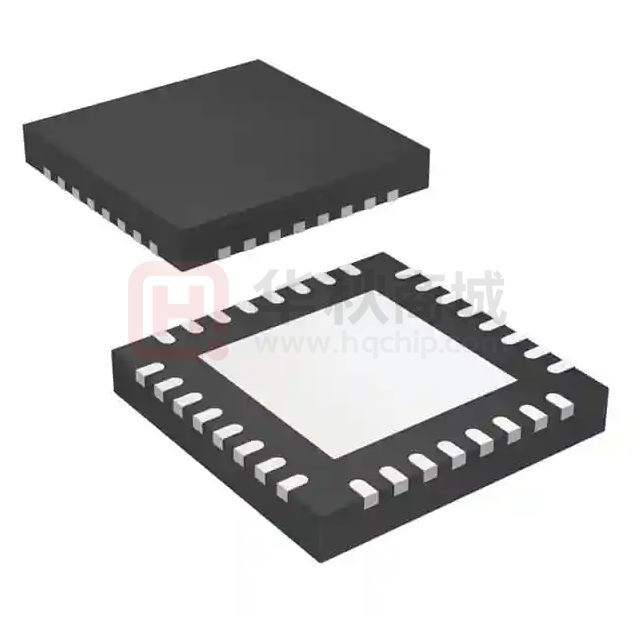


 工商网监
湘ICP备2023018690号
工商网监
湘ICP备2023018690号
