SIG5530
24-bit Sigma-Delta ADC with Gain=64 Ultra-Low-Noise Amplifier
FEATURES
DESCRIPTION
Amplifier Gain: 64
Selectable Data Rates: 1.875 to 3840SPS
RMS Noise: 16nV at 7.5SPS
20.4 Noise-Free Bits at 1.875SPS
Offset Drift: 5nV/°C
Gain Drift: 1ppm/°C
Integral Non-Linearity: 3ppm
Internal or External Clock
Burnout Current Sources
Parity Check
Power Supply
AVDD: 4.75V to 5.25V or ±2.5V
DVDD: 2.7V to 5.25V
Current: 4.0mA
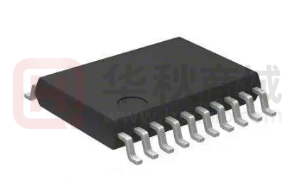
Package: 20-lead TSSOP
The SIG5530 is a low noise, low drift, and high-resolution 24-bit
analog-to-digital converter (ADC) with integrated gain amplifier
that offers high-accuracy measurement solutions for bridge
sensors.
The device contains an ultra-low-noise amplifier with fixed gain
64, a delta-sigma (Δ-Σ) modulator, and a programmable
SINC3/SINC1 digital filter. The output data rate from the device
can be configured to 1.875, 3.75, 7.5, 15, 30, 60, 120, 240, 480,
960, 1920, and 3840SPS. Burnout current sources are provided
at the analog inputs for sensor connection diagnosis.
Offset and gain calibration registers are provided with calibration
command or direct register write to calibrate the ADC errors or
overall system errors. SPI-compatible interface is used for
device configuration and parity check is provided for data
integrity.
The on-chip oscillator, an external clock, or an external crystal
can be used as the clock source to the device.
The device can operate with bipolar ±2.375V to ±2.625V analog
power supplies, or with a single 4.75V to 5.25V analog power
supply.
APPLICATIONS
Weigh Scales
Strain Gauges
Pressure Sensors
Industrial Process Control
The SIG5530 is available in 20-lead TSSOP package. These
devices are fully specified over the -40°C to +125°C temperature
range.
Function Block Diagram
AVDD
TSSOP-20
DVDD
VREF+ VREF-
AIN1+
1
20
AIN2+
AIN1-
2
19
AIN2-
C1
3
18
VREF+
C2
4
17
VREF-
VA+
5
16
DGND
VA-
6
15
VD+
A0/PDSW
7
14
CSn
A1
8
13
SDI
OSC2
9
12
SDO
OSC1
10
11
SCLK
REFERENCE
DETECT
BUF
AIN1+
MUX
AIN1AIN2+
AIN2-
PGA
Digital
Filter
Internal
Oscillator
A0/PDSW
AVSS
C1 C2
CSn
DIN
DOUT/DRDYn
SCLK
A1
Gain=64
TEMP
Sensor
May 2022
ΔΣ ADC
Serial
Interface
And
Control
Logic
Clock
Circuitry
OSC2
OSC1
DGND
Signal Micro Incorporated
http://www.signal-micro.cn
SIG5530
TSSOP-20
�SIG5530
PIN CONFIGURATION and DESCRIPTIONS
TOP VIEW (Not To Scale)
PIN
AIN1+
1
20
AIN2+
AIN1-
2
19
AIN2-
C1
3
18
VREF+
C2
4
17
VREF-
AVDD
5
16
DGND
AVSS
6
15
DVDD
A0/PDSW
7
14
CSn
DIN
SIG5530
TSSOP-20
A1
8
13
OSC2
9
12
DOUT/DRDYn
OSC1
10
11
SCLK
No.
1
2
NAME
AIN1+
AIN1-
FUNCTION
DESCRIPTION
Analog Input
Analog Input
3
C1
Analog Output
4
C2
Analog Output
5
AVDD
Analog
Positive analog input channel 1.
Negative analog input channel 1.
Amplifier analog output. Connect a COG cap with size 4.7~22nF between
C1 and C2.
Amplifier analog output. Connect a COG cap with size 4.7~22nF between
C1 and C2.
Positive analog power supply. 4.75V to 5.25V relative to AVSS.
6
7
8
AVSS
A0/PDSW
A1
Negative analog power supply.
Analog logic output or bridge power down switch.
Analog logic output.
9
OSC2
10
OSC1
Analog
Analog Output
Analog Output
Digital
Input/Output
Digital Input
11
12
SCLK
DOUT/DRDYn
Digital Input
Digital Output
Serial data clock.
Serial data output and data ready indicator.
13
14
DIN
CSn
Digital Input
Digital Input
15
16
DVDD
DGND
Digital
Digital
17
18
REFREF+
Analog Input
Analog Input
Negative reference input.
Positive reference input.
19
20
AIN2AIN2+
Analog Input
Analog Input
Negative analog input channel 2.
Positive analog input channel 2.
May 2022
Master clock input or Crystal Connection.
Crystal Connection.
Serial data input.
Serial chip select. Active low.
Digital power supply, 2.7V to 5.25V. DVDD is independent of AVDD.
Digital ground reference point.
Signal Micro Incorporated
http://www.signal-micro.cn
2
�SIG5530
PACKAGE/ORDERING INFORMATION
MODEL
PACKAGE DESCRIPTION
SPECIFIED TEMPERATURE
RANGE
ORDERING NUMBER
PACKING OPTION
SIG5530
TSSOP-20
-40°C to +125°C
SIG5530-ITSP20-RL
Reel, 4500
SPECIFICATIONS
Absolute Maximum Ratings
Over operating free-air temperature range, unless otherwise noted.(1)
Voltage
Current
Temperature
MIN
MAX
UNIT
AVDD to AVSS
–0.3
6.5
V
AVSS to DGND
–3
0.3
V
DVDD to DGND
–0.3
6.5
V
V
Analog input
VAVSS – 0.3
VAVDD + 0.3
Digital input
VDGND – 0.3
VDVDD + 0.3
V
Input current
–10
10
mA
Junction (TJ)
–50
150
°C
Storage (Tstg)
-60
150
°C
(1) Stresses beyond those listed under Absolute Maximum Ratings may cause permanent damage to the device. These is a stress rating only;
functional operation of the device at these or any other conditions above those indicated in the operational section of this specification is not
implied. Exposure to absolute maximum rating conditions for extended periods may affect device reliability.
ESD Ratings
SYMBOL
PARAMTER
CONDITION
VALUE
UNIT
HBM
Human-body Model
CDM
Charged-device model
ANSI/ESDA/JEDEC JS-001
±4000
V
JEDEC EIA/JS-002-2022
±2000
V
This integrated circuit can be damaged by ESD. Signal Micro recommends that all integrated circuits be handled with appropriate
precautions. Failure to observe proper handling and installation procedures can cause damage. ESD damage can range from
subtle performance degradation to complete device failure. Precision integrated circuits may be more susceptible to damage
because very small parametric changes could cause the device not to meet its published specifications.
May 2022
Signal Micro Incorporated
http://www.signal-micro.cn
3
�SIG5530
Electrical Characteristics
Minimum/Maximum specifications apply from -40˚C to +125˚C. Typical specifications are at +25˚C. All specification are at
VAVDD=5V, VAVSS=0V, VDVDD=3.3V, VREF=2.5V, fCLK=4.9152MHz, data rate=60SPS, unless otherwise noted.
TEST CONDITION
OR NOTES
PARAMETER
MIN(1)
TYP
MAX(1)
UNITS
+VREF/(2xGain)
VAVDD – 0.5
VAVDD – 0.5 –
|VINMAX|·32
V
V
ANALOG INPUTS
Differential Input Voltage
Absolute Input Voltage
VIN = VINP – VINN
Common Mode Input Range
GAIN=64
–VREF/(2xGain)
VAVSS + 0.5
VAVSS + 0.5 +
|VINMAX|·32
Absolute Input Current
±2
V
nA
SYSTEM PERFORMANCE
Amplifier Gain
64
V/V
Resolution
24
Bits
Data Rate
1.875
Noise
3840
SPS
See Noise Table
Integral Nonlinearity (INL)
±3
ppm
Offset Error
±3
μV
Offset Drift vs. Temperature
±5
nV/°C
±0.01
%
Gain Error
Gain Drift vs. Temperature
Common Mode Rejection
(CMRR)
(2)
Power Supply Rejection
(PSRR)
REFERENCE INPUT
Differential Reference Voltage
(VREF)
Absolute Negative Reference
Voltage (VREFN)
Absolute Positive Reference
Voltage (VREFP)
Average Voltage Input Current
fIN=50/60Hz, data
rate=960SPS
AVDD, AVSS
-5
±1
100
120
5
ppm/°C
dB
75
90
dB
DVDD
80
120
dB
VREF = VREFP – VREFN
0.5
VAVDD – VAVSS + 0.1
V
VAVSS – 0.05
VREFP – 0.5
V
VREFN + 0.5
VAVDD + 0.05
V
300
nA
1
μA
Burnout Current Sources
Current Setting
ADC CLOCK
External Clock
Internal Oscillator
Frequency Range
Duty Cycle
1
4.9152
40%
Nominal Frequency
5
4.9152
Accuracy
–3%
High-level Output Voltage (VOH)
IOH = 4mA
0.8·VDVDD
Low-level Output Voltage (VOL)
IOL = –4mA
MHz
60%
±0.5%
MHz
3%
DIGITAL INPUT/OUTPUT
V
0.2·VDVDD
V
High-level Input Voltage (VIH)
0.7·VDVDD
VDVDD
V
Low-level Input Voltage (VIL)
VDGND
0.3·VDVDD
V
Input Hysteresis
0.5
Input Leakage
V
±10
μA
POWER SUPPLY
AVSS Voltage (VAVSS)
–2.625
0
V
AVDD Voltage (VAVDD)
VAVSS + 4.75
VAVSS + 5.25
V
DVDD Voltage (VDVDD)
2.7
5.25
V
4.5
mA
AVDD, AVSS Current (IAVDD)
May 2022
Active Mode
3.6
Sleep Mode
1
Signal Micro Incorporated
http://www.signal-micro.cn
μA
4
�SIG5530
DVDD Current (IDVDD)
Total Power Dissipation
Active Mode
0.4
Sleep Mode
40
0.6
mA
μA
Active Mode
20
mW
Sleep Mode
0.15
mW
TEMPERATURE RANGE
Specified temperature range
–40
125
°C
Operating temperature range
–50
125
°C
Storage temperature range
–60
150
°C
(1) Compliance to datasheet limits is assured by one or more methods: production test, characterization and/or design.
(2) Power supply rejection is specified DC change in voltage.
May 2022
Signal Micro Incorporated
http://www.signal-micro.cn
5
�SIG5530
Timing Requirements: Serial Interface
Over the operating ambient temperature range and DVDD = 2.7V to 5.25V, unless otherwise noted.
t7
CSn
t1
t5
B7
DOUT
B6
B5
B4
B3
B2
B1
B0
t2
t8
t6
t3
SCLK
t4
t9
t10
DIN
B7
B6
B5
B4
B3
B2
B1
B0
Figure 1. Serial Interface Timing Requirements
SYMBOL
t1
t2
t3
t4
DESCRIPTION
CSn falling edge to valid DOUT/DRDYn: propagation delay(1)
SCLK falling edge to valid DOUT/DRDYn: propagation delay(1)
SCLK high pulse width
MIN
MAX
20
20
50
UNIT
ns
ns
ns
SCLK low pulse width
50
ns
SCLK period
100
106
ns
20
ns
t5
CSn rising edge to DOUT high impedance: propagation delay
t6
Last SCLK falling edge to CSn rising edge: delay time
20
ns
t7
CSn high pulse width
50
ns
50
ns
time(2)
t8
CSn falling edge to first SCLK rising edge: setup
t9
Valid DIN to SCLK rising edge: setup time
20
ns
t10
Valid DIN to SCLK rising edge: hold time
20
ns
(1) DOUT load = 20pF || 100k Ω to DGND.
(2) CSn can be tied low.
May 2022
Signal Micro Incorporated
http://www.signal-micro.cn
6
�SIG5530
NOISE PERFORMANCE
The noise performance of the ADC is affected by amplifier gain, data rate, and digital filter setting. The following tables
show the rms noise and peak-to-peak noise for SINC3 and SINC1 filters. The effective number of bits (ENOB) and
noise-free bits are also listed according to Equation (1) and Equation (2):
ENOB= log 2 (2×VREF ⁄Gain⁄VRMS )
Noise Free Bits= log 2 �2×VREF ⁄Gain⁄Vp-p �
(1)
(2)
The noise data listed in the table are typical and are generated from continuous ADC readings with differential input
voltage of 0 V.
Table 1. ADC Noise in µVRMS (µVPP) at TA = 25°C, VAVDD = 5 V, VAVSS = 0 V, VREF = 2.5 V, SINC3 Filter
Data Rate(SPS)
1.875
3.75
7.5
15
30
60
120
240
480
960
1920
3840
GAIN=64
0.008(0.050)
0.011(0.070)
0.016(0.099)
0.023(0.140)
0.032(0.198)
0.045(0.280)
0.064(0.396)
0.091(0.561)
0.128(0.793)
0.182(1.12)
0.255(1.55)
0.357(2.47)
Table 2. ADC ENOB (Noise Free Bits) at TA = 25°C, VAVDD = 5 V, VAVSS = 0 V, VREF = 5 V, SINC3 Filter
Data Rate(SPS)
1.875
3.75
7.5
15
30
60
120
240
480
960
1920
3840
May 2022
GAIN=64
23.2(20.4)
22.7(19.9)
22.2(19.4)
21.7(18.9)
21.2(18.4)
20.7(17.9)
20.2(17.4)
19.7(16.9)
19.2(16.4)
18.7(15.9)
18.2(15.3)
17.7(14.9)
Signal Micro Incorporated
http://www.signal-micro.cn
7
�SIG5530
Table 3. ADC Noise in µVRMS (µVPP) at TA = 25°C, VAVDD = 5 V, VAVSS = 0 V, VREF = 2.5 V, SINC1 Filter
Data Rate(SPS)
1.875
3.75
7.5
15
30
60
120
240
480
960
1920
3840
GAIN=64
0.010(0.062)
0.014(0.088)
0.020(0.125)
0.029(0.176)
0.041(0.249)
0.057(0.352)
0.081(0.498)
0.115(0.705)
0.163(0.996)
0.230(1.41)
0.317(2.20)
0.397(3.00)
Table 4. ADC ENOB (Noise Free Bits) at TA = 25°C, VAVDD = 5 V, VAVSS = 0 V, VREF = 5 V, SINC1 Filter
Data Rate(SPS)
1.875
3.75
7.5
15
30
60
120
240
480
960
1920
3840
May 2022
GAIN=64
22.8(20.1)
22.3(19.6)
21.8(19.1)
21.3(18.6)
20.8(18.1)
20.3(17.6)
19.8(17.1)
19.3(16.6)
18.8(16.1)
18.3(15.6)
17.9(15.0)
17.5(14.9)
Signal Micro Incorporated
http://www.signal-micro.cn
8
�SIG5530
REGISTER MAPS
There are total three 24-bit registers inside the device. These registers are used to configure and control the ADC to
the desired mode of operation. These registers can be accessed through the SPI-compatible serial interface by using
register read and write commands. At power-on or reset, the registers default to their initial settings, as shown in the
Reset Value column of Table 5.
Table 5. Register map
ADDR.
RS[2:0]
NAME
RESET
VALUE
3’b001
OFFSET
0x00000000
3’b010
GAIN
0x01000000
3’b011
CONF
0x00000000
BIT 31
BIT 23
BIT 15
BIT 7
BIT 30
BIT 22
BIT 14
BIT 6
BIT 29
BIT 21
BIT 13
BIT 5
BIT 28
BIT 27
BIT 20
BIT 19
BIT 12
BIT 11
BIT 4
BIT 3
OFFSET[31:24]
OFFSET[23:16]
OFFSET[15:8]
OFFSET[7:0]
GAIN[23:16]
GAIN[23:16]
GAIN[15:8]
GAIN[7:0]
BIT26
BIT18
BIT10
BIT 2
BIT 25
BIT 17
BIT 9
BIT 1
BIT 24
BIT 16
BIT 8
BIT 0
PSS
PDW
RS
RV
SHORT
A0_PSW
VRS
A0
0
0
0
FRS
FILTER
TPS
0
0
CHKSUM
DR[3]
LATENCY
DR[2]
CLK1
DR[1]
CLK0
DR[0]
CS1]
FORMAT
CS[0]
BCS
0
DT
0
A1
OFFSET Register
Table 6. OFFSET Register (Address = 3’b001)
BIT 31
BIT 30
BIT 29
BIT 28
BIT 27
BIT26
BIT 25
BIT 24
BIT 23
BIT 22
BIT 21
BIT 20
BIT 19
BIT18
BIT 17
BIT 16
BIT 15
BIT 14
BIT 13
BIT 12
BIT 11
BIT10
BIT 9
BIT 8
BIT 7
BIT 6
BIT 5
BIT 4
BIT 3
BIT 2
BIT 1
BIT 0
OFFSET[31]
OFFSET[30]
OFFSET[29]
OFFSET[28]
OFFSET[27]
OFFSET[26]
OFFSET[25]
OFFSET[24]
OFFSET[23]
OFFSET[22]
OFFSET[21]
OFFSET[20]
OFFSET[19]
OFFSET[18]
OFFSET[17]
OFFSET[16]
OFFSET[15]
OFFSET[14]
OFFSET[13]
OFFSET[12]
OFFSET[11]
OFFSET[10]
OFFSET[9]
OFFSET[8]
OFFSET[7]
OFFSET[6]
OFFSET[5]
OFFSET[4]
OFFSET[3]
OFFSET[2]
OFFSET[1]
OFFSET[0]
Power-On/Reset value = 0x00000000
Bits
Bit Name
Access
Reset
Description
31:0
OFFSET[31:0]
R/W
0x00000000
Offset Calibration Bits: The 32-bit word is signed number in 2’s
complement format. See Calibration section for more information.
GAIN Register
Table 7. GAIN Register (Address = 3’b010)
BIT 31
BIT 30
BIT 29
BIT 28
BIT 27
BIT26
BIT 25
BIT 24
BIT 23
BIT 22
BIT 21
BIT 20
BIT 19
BIT18
BIT 17
BIT 16
BIT 15
BIT 14
BIT 13
BIT 12
BIT 11
BIT10
BIT 9
BIT 8
BIT 7
BIT 6
BIT 5
BIT 4
BIT 3
BIT 2
BIT 1
BIT 0
GAIN[31]
GAIN[30]
GAIN[29]
GAIN[28]
GAIN[27]
GAIN[26]
GAIN[25]
GAIN[24]
GAIN[23]
GAIN[22]
GAIN[21]
GAIN[20]
GAIN[19]
GAIN[18]
GAIN[17]
GAIN[16]
GAIN[15]
GAIN[14]
GAIN[13]
GAIN[12]
GAIN[11]
GAIN[10]
GAIN[9]
GAIN[8]
GAIN[7]
GAIN[6]
GAIN[5]
GAIN[4]
GAIN[3]
GAIN[2]
GAIN[1]
GAIN[0]
Power-On/Reset value = 0x01000000
May 2022
Signal Micro Incorporated
http://www.signal-micro.cn
9
�SIG5530
Bits
Bit Name
Access
Reset
Description
31:0
GAIN[31:0]
R/W
0x01000000
Gain Calibration Bits: The 32-bit word is unsigned positive number
in binary format. See Calibration section for more information.
Configuration Register (CONF)
Table 8. CONF Register (Address = 3’b011)
BIT 31
BIT 30
BIT 29
BIT 28
BIT 27
BIT26
BIT 25
BIT 24
BIT 23
BIT 22
BIT 21
BIT 20
BIT 19
BIT18
BIT 17
BIT 16
BIT 15
BIT 14
BIT 13
BIT 12
BIT 11
BIT10
BIT 9
BIT 8
BIT 7
BIT 6
BIT 5
BIT 4
BIT 3
BIT 2
BIT 1
BIT 0
PSS
PDW
RS
RV
SHORT
A0_PSW
VRS
A1
A0
0
0
0
FRS
FILTER
TPS
0
0
DR[3]
DR[2]
DR[1]
DR[0]
FORMAT
BCS
DT
CHKSUM
LATENCY
CLK1
CLK0
CS1]
CS[0]
0
0
Power-On/Reset value = 0x00000000
Bits
Bit Name
Access
Reset
Description
31
PSS
R/W
1’b0
Power Save Select:
0: Standby Mode (default)
1: Sleep Mode
30
PDW
R/W
1’b0
Power Down Mode:
0: Normal Mode (default)
1: Power Down Mode
29
RS
R/W
1’b0
Reset System:
0: Normal Operation (default)
1: Activate a Reset cycle.
28
RV
R
1’bx
Reset Indicator: Read only. Bit is cleared to logic zero after the
CONF register is read.
0: Normal Operation (default)
1: System was reset.
27
SHORT
R/W
1’b0
Input Short:
0: Normal Input (default)
1: Analog Inputs are disconnected from the pins and shorted
internally to mid-supply (VAVDD+VAVSS)/2.
26
A0_PSW
R/W
1’b0
Bridge Power-down Switch Function: When this bit is set to 1,
the output latch bit A0 is served as the switch control bit. The switch
is closed to short pin A0 to DVSS with low on-resistor of typical 3
Ohms if the output latch bit is set to 1. The switch is open if the
output latch bit is cleared. The switch remains active in standby
mode and is forced to open in sleep mode.
0: Disabled (default)
1: Enabled.
25
VRS
R/W
1’b0
Voltage Reference Select: The input full-scale range is
[-VREF/(2xgain), VREF/(2xgain)] with VRS=0, and is
[-VREF/gain, VREF/gain] with VRS=1.
0: 2.5V


 工商网监
湘ICP备2023018690号
工商网监
湘ICP备2023018690号
