LM331
General-Purpose High-Voltage Open-Drain
Output Single Comparator
1 FEATURES
•
Supply Range: +3V to +32V
•
Low Supply Current
65μA (TYP) per channel at VS = 5V
•
Low Output Saturation Voltage
•
Open-Drain Output for Maximum Flexibility
•
SPECIFIED UP TO +125°C
•
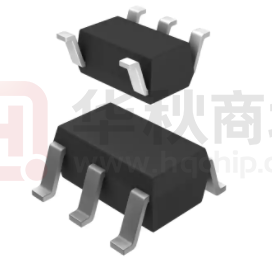
Micro SIZE PACKAGES: SOT23-5
2 APPLICATIONS
•
Hysteresis Comparators
•
Factory Automation & Control
•
Industrial Equipment
•
Test and Measurement
•
Cordless Power Tool
•
Vacuum Robot
•
Wireless Infrastructure
3 DESCRIPTIONS
The LM331 is the single comparator version, and the
outputs can be connected to other open-collector
outputs to achieve wired-AND relationships. It can
operate from 3V to 32V, and have low power consuming
65uA (TYP) per channel.
The LM331 consist one voltage comparators that are
designed to operate from a single power supply over a
wide range of voltages. Quiescent current is
independent of the supply voltage. The device is the
most cost-effective solutions for applications where low
offset voltage, high supply voltage capability, low supply
current, and space saving are the primary specifications
in circuit design for portable consumer products.
The LM331 is available in Green SOT23-5 packages. It
operates over an ambient temperature range of -40°C
to +125°C.
Device Information (1)
PART
NUMBER
LM331
(1)
REV A.2
PACKAGE
BODY SIZE (NOM)
SOT23-5
2.90mm×1.60mm
For all available packages, see the orderable addendum at the
end of the data sheet.
1 / 14
www.run-ic.com
�LM331
Table of Contents
1 FEATURES .......................................................................................................................................................1
2 APPLICATIONS ................................................................................................................................................1
3 DESCRIPTIONS ................................................................................................................................................1
4 Revision History ..............................................................................................................................................3
5 PACKAGE/ORDERING INFORMATION (1) ......................................................................................................4
6 Pin Configuration and Functions (Top View) ...............................................................................................5
7 SPECIFICATIONS ............................................................................................................................................6
7.1 Absolute Maximum Ratings ........................................................................................................................6
7.2 ESD Ratings................................................................................................................................................6
7.3 Recommended Operating Conditions .........................................................................................................6
7.4 Thermal Information: LM331 .......................................................................................................................7
7.5 ELECTRICAL CHARACTERISTICS ...........................................................................................................8
7.6 TYPICAL CHARACTERISTICS ..................................................................................................................9
8 Detailed Description ..................................................................................................................................... 10
8.1 Overview .................................................................................................................................................. 10
9 Application and Implementation ................................................................................................................. 11
9.1 Application Information ............................................................................................................................ 11
9.2 Typical Application ................................................................................................................................... 11
9.3 Detailed Design Procedure ...................................................................................................................... 11
9.4 Input Voltage Range ................................................................................................................................ 11
10 PACKAGE OUTLINE DIMENSIONS ........................................................................................................... 12
11 TAPE AND REEL INFORMATION .............................................................................................................. 13
2 / 14
www.run-ic.com
�LM331
4 Revision History
Note: Page numbers for previous revisions may different from page numbers in the current version.
VERSION
Change Date
A.0
2020/02/11
A.1
2022/02/23
A.2
2022/07/15
Change Item
Pre version completed
1.Modify ELECTRICAL CHARACTERISTICS and TYPICAL CHARACTERISTICS
2.Add TAPE AND REEL INFORMATION
Change Supply Range: +3V to +32V
3 / 14
www.run-ic.com
�LM331
5 PACKAGE/ORDERING INFORMATION (1)
Orderable
Device
LM331BXF
LM331CXF
-40°C ~+125°C
Device
Marking (2)
331B
Tape and Reel,3000
-40°C ~+125°C
331C
Tape and Reel,3000
Package Type
Pin
Channel
Op Temp(°C)
SOT23-5
5
1
SOT23-5
5
1
Package Qty
NOTE:
(1) This information is the most current data available for the designated devices. This data is subject to change without notice and revision
of this document. For browser-based versions of this data sheet, refer to the right-hand navigation.
(2) There may be additional marking, which relates to the lot trace code information(data code and vendor code),the logo or the
environmental category on the device.
4 / 14
www.run-ic.com
�LM331
6 Pin Configuration and Functions (Top View)
LM331C
LM331B
V-
2
-IN
3
5
V+
-IN
1
-
V-
2
4
OUT
+IN
3
SOT23-5
5
V+
4
OUT
-
+
1
+
+IN
SOT23-5
Pin Description
PIN SOT23-5
I/O (1)
NAME
(1)
DESCRIPTION
LM331B
LM331C
+IN
1
3
I
Noninverting input
V-
2
2
P
Negative (lowest) power supply
-IN
3
1
I
Inverting input
OUT
4
4
O
Output
V+
5
5
P
Positive (highest) power supply
I=Input, O=Output, P=Power
5 / 14
www.run-ic.com
�LM331
7 SPECIFICATIONS
7.1 Absolute Maximum Ratings
Over operating free-air temperature range (unless otherwise noted) (1)
MIN
MAX
Supply, VS=(V+) - (V-)
Voltage
Input pin (IN+, IN-)
36
(2)
Signal output pin (3)
(V-)-0.3
(V+) +0.3
(V-)-0.3
(V+) +0.3
-10
10
mA
55
mA
Signal input pin (IN+, IN-) (2)
Current
Signal output pin
(3)
-55
Output short-circuit (4)
Junction, TJ
V
Continuous
Operating range, TA
Temperature
UNIT
(5)
Storage, Tstg
-40
125
-40
150
-65
150
°C
(1) Stresses above these ratings may cause permanent damage. Exposure to absolute maximum conditions for extended periods may
degrade device reliability. These are stress ratings only, and functional operation of the device at these or any other conditions beyond
those specified is not implied.
(2) Input terminals are diode-clamped to the power-supply rails. Input signals that can swing more than 0.3V beyond the supply rails should
be current-limited to 10mA or less.
(3) Output terminals are diode-clamped to the power-supply rails. Output signals that can swing more than 0.3V beyond the supply rails
should be current-limited to ±55mA or less.
(4) Short-circuit from output to VS can cause excessive heating and eventual destruction.
(5) The maximum power dissipation is a function of TJ(MAX), RθJA, and TA. The maximum allowable power dissipation at any ambient
temperature is PD = (T J(MAX) - TA) / RθJA. All numbers apply for packages soldered directly onto a PCB.
7.2 ESD Ratings
The following ESD information is provided for handling of ESD-sensitive devices in an ESD protected area only.
VALUE
V(ESD)
Electrostatic discharge
Human-Body Model (HBM), per ANSI/ESDA/JEDEC JS001, all pins (1)
Charged Device Model (CDM), per JEDEC specification
JESD22-C101, all pins (2)
UNIT
±2000
V
±1000
(1) JEDEC document JEP155 states that 500V HBM allows safe manufacturing with a standard ESD control process.
(2) JEDEC document JEP157 states that 250V CDM allows safe manufacturing with a standard ESD control process.
ESD SENSITIVITY CAUTION
ESD damage can range from subtle performance degradation to complete device failure. Precision integrated circuits may
be more susceptible to damage because very small parametric changes could cause the device not to meet its published
specifications.
7.3 Recommended Operating Conditions
Over operating free-air temperature range (unless otherwise noted)
MIN
Supply voltage,VS= (V+) - (V-)
Single-supply
Dual-supply
6 / 14
NOM
MAX
3
32
±1.5
±16
UNIT
V
www.run-ic.com
�LM331
7.4 Thermal Information: LM331
LM331
THERMAL METRIC (1)
5PINS
UNIT
SOT23-5
RϴJA
Junction-to-ambient thermal resistance
273.8
°C/W
RϴJC(top)
Junction-to-case(top) thermal resistance
126.8
°C/W
RϴJB
Junction-to-board thermal resistance
85.9
°C/W
ѰJT
Junction-to-top characterization parameter
10.9
°C/W
ѰJB
Junction-to-board characterization parameter
84.9
°C/W
RϴJC(bot)
Junction-to-case(bottom) thermal resistance
N/A
°C/W
(1) Thermal resistance varies with operating conditions.
7 / 14
www.run-ic.com
�LM331
7.5 ELECTRICAL CHARACTERISTICS
(At TA = +25ºC, VCM=(VS/2), VS=5V, unless otherwise noted.)
LM331
PARAMETER
CONDITIONS
UINTS
MIN
VS
Operating Voltage Range
IQ
Quiescent Current
VOS
Input offset voltage
IB
Input Bias Current
3
VS=5V, no load
VS=32V, no load,
TA=-40C to +125C
VS=5V to 32V
VS=5V to 32V
TA=-40C to +125C
TA=25C
65
-7.5
±5
-10
VCM
Common-Mode Voltage Range
10
AVD
Large signal differential voltage
amplification
VOL
Low-Level output voltage
IOL
Output Current(sinking)
TA=-40C to +125C
High-Level Output Leakage Current
VS=3V to 32V
VS=3V to 32V
TA=-40C to +125C
VS=15V, Vo=1.4V to
11.4V
RL≥15k to (V+)
Isink≤4mA, VID=-1V
VO=1.5V; VID=-1V;
VS=5V
(V+) =Vo=5V; VID=1V
(V+) =Vo=32V; VID=1V
uA
7.5
10
10
pA
100
nA
50
pA
100
nA
(V+)-1.5
(V-)+0.5
(V+)-2.0
200
300
mV
50
(V-)+0.5
50
V
100
100
TA=25C
Input Offset Current
MAX
32
TA=-40C to +125C
IOS
ILEAK
TYP
V
V/mV
360
15
mV
mA
2
20
nA
4
50
nA
Switching Characteristics
VS=5V
TPHL
Propagation Delay H To L
VS=32V
VS=5V
TPLH
Propagation Delay L To H
VS=32V
RPU=5.1KΩ, Overdrive
=10mV
RPU=5.1KΩ, Overdrive
=100mV
RPU=5.1KΩ, Overdrive
=10mV
RPU=5.1KΩ, Overdrive
=100mV
RPU=5.1KΩ, Overdrive
=10mV
RPU=5.1KΩ, Overdrive
=100mV
RPU=5.1KΩ, Overdrive
=10mV
RPU=5.1KΩ, Overdrive
=100mV
8 / 14
0.5
0.3
0.64
0.5
us
1.5
0.3
1.5
0.25
www.run-ic.com
�LM331
7.6 TYPICAL CHARACTERISTICS
Input Bias Current(pA)
Total Supply Current(uA)
NOTE: The graphs and tables provided following this note are a statistical summary based on a limited number of samples
and are provided for informational purposes only.
At TA = +25C, VS=5V, RPULLUP=5.1K VCM = Vs/2, CL=15pF, VOVERDRIVE=100mV, unless otherwise noted.
100K
90
No Load,Output High
80
10K
70
60
50
40
30
20
-40°C
25°C
125°C
10
0
2
5
8
10
1
0.1
-40 -20
Supply Voltage(V)
0
20 40 60 80 100 120 140
Temperature(℃)
Figure 2. INPUT BIAS CURRENT vs
TEMPERATURE
0.6
3.5
VS=5V
VS=5V
3
0.5
2.5
Time(us)
0.4
Time(us)
100
11 14 17 20 23 26 29 32
Figure 1. Total Supply Current vs Supply
Voltage
0.3
0.2
2
1.5
1
0.1
0.5
0
0
0
0
50 100 150 200 250 300 350 400
Overdrive(mV)
Figure 3. Response Time vs Input Overdrives
Negative Transition
50
100 150 200 250 300 350 400
Overdrive(mV)
Figure 4. Response Time vs Input Overdrives
Positive Transition
3.5
0.8
VS=32V
0.7
VS=32V
3
0.6
2.5
0.5
Time(us)
Time(us)
1K
0.4
0.3
2
1.5
1
0.2
0.5
0.1
0
0
0
0
50 100 150 200 250 300 350 400
Overdrive(mV)
Figure 5. Response Time vs Input Overdrives
Negative Transition
50 100 150 200 250 300 350 400
Overdrive(mV)
Figure 6. Response Time vs Input Overdrives
Positive Transition
9 / 14
www.run-ic.com
�LM331
8 Detailed Description
8.1 Overview
The LM331 family of comparators can operate up to 32V on the supply pin. This standard device has proven
ubiquity and versatility across a wide range of applications. This is due to its low power and high speed. The
open-drain output allows the user to configure the output's logic low voltage (VOL) and can be utilized to enable
the comparator to be used in AND functionality.
V+
IN+
IN-
+
OUT
VFigure 7. Functional Block Diagram
10 / 14
www.run-ic.com
�LM331
9 Application and Implementation
Information in the following applications sections is not part of the RUNIC component specification, and RUNIC
does not warrant its accuracy or completeness. RUNIC’s customers are responsible for determining suitability
of components for their purposes. Customers should validate and test their design implementation to confirm
system functionality.
9.1 Application Information
LM331 is typically used to compare a single signal to a reference or two signals against each other. Many users
take advantage of the open drain output (logic high with pull-up) to drive the comparison logic output to a logic
voltage level to an MCU or logic device. The wide supply range and high voltage capability makes this
comparator optimal for level shifting to a higher or lower voltage.
9.2 Typical Application
VLOGIC
VLOGIC
VSUP
VIN
+
VSUP
RPULLUP
VIN+
LM331
Vref
RPULLUP
+
LM331
CL
VIN-
CL
Figure 8. Single-Ended and Differential Comparator Configurations
9.3 Detailed Design Procedure
When using the device in a general comparator application, determine the following:
• Input Voltage Range
• Minimum Overdrive Voltage
• Output and Drive Current
• Response Time
9.4 Input Voltage Range
When choosing the input voltage range, the input common mode voltage range (VICR) must be taken in to
account. If temperature operation is below 25°C the VICR can range from 0 V to V S– 2.0 V. This limits the input
voltage range to as high as VS– 2.0 V and as low as 0 V. Operation outside of this range can yield incorrect
comparisons.
11 / 14
www.run-ic.com
�LM331
10 PACKAGE OUTLINE DIMENSIONS
SOT23-5
D
1.90
b
2.59
E1
E
0.99
0.95
0.69
e
e1
RECOMMENDED LAND PATTERN (Unit: mm)
0.2
A A2
c
θ
L
A1
Dimensions In Millimeters
Dimensions In Inches
Symbol
Min
Max
Min
Max
A
1.050
1.250
0.041
0.049
A1
0.000
0.100
0.000
0.004
A2
1.050
1.150
0.041
0.045
b
0.300
0.500
0.012
0.020
c
0.100
0.200
0.004
0.008
D
2.820
3.020
0.111
0.119
E
1.500
1.700
0.059
0.067
E1
2.650
2.950
0.104
0.116
e
0.950(BSC)
0.037(BSC)
e1
1.800
2.000
0.071
0.079
L
0.300
0.600
0.012
0.024
θ
0°
8°
0°
8°
NOTE:
A. All linear dimension is in millimeters.
B. This drawing is subject to change without notice.
C. Body dimensions do not include mold flash or protrusion. Mold flash and protrusion shall not exceed 0.15 per side.
D. BSC: Basic Dimension. Theoretically exact value shown without tolerances.
12 / 14
www.run-ic.com
�LM331
11 TAPE AND REEL INFORMATION
REEL DIMENSIONS
TAPE DIMENSION
Reel
Diameter
Reel Width(W1)
DIRECTION OF FEED
NOTE: The picture is only for reference. Please make the object as the standard.
KEY PARAMETER LIST OF TAPE AND REEL
Package
Type
Reel
Diameter
SOT23-5
7’’
Reel
Width
(mm)
9.5
A0
(mm)
B0
(mm)
K0
(mm)
P0
(mm)
P1
(mm)
P2
(mm)
W
(mm)
Pin1
Quadrant
3.20
3.20
1.40
4.0
4.0
2.0
8.0
Q3
NOTE:
1. All dimensions are nominal.
2. Plastic or metal protrusions of 0.15mm maximum per side are not included.
13 / 14
www.run-ic.com
�LM331
IMPORTANT NOTICE AND DISCLAIMER
Jiangsu RUNIC Technology Co., Ltd. will accurately and reliably provide technical and reliability data (including
data sheets), design resources (including reference designs), application or other design advice, WEB tools,
safety information and other resources, without warranty of any defect, and will not make any express or implied
warranty, including but not limited to the warranty of merchantability Implied warranty that it is suitable for a
specific purpose or does not infringe the intellectual property rights of any third party.
These resources are intended for skilled developers designing with RUNIC products You will be solely
responsible for: (1) Selecting the appropriate products for your application; (2) Designing, validating and testing
your application; (3) Ensuring your application meets applicable standards and any other safety, security or
other requirements; (4) RUNIC and the RUNIC logo are registered trademarks of RUNIC INCORPORATED. All
trademarks are the property of their respective owners; (5) For change details, review the revision history
included in any revised document. The resources are subject to change without notice. Our company will not
be liable for the use of this product and the infringement of patents or third-party intellectual property rights due
to its use.
14 / 14
www.run-ic.com
�


 工商网监
湘ICP备2023018690号
工商网监
湘ICP备2023018690号
