SIG2012
SIG2012: 10SPS, 20-bit Sigma-Delta ADC with PGA
FEATURES
DESCRIPTION
PGA Gain: 128 or 256
Data Rates: 10SPS
RMS Noise: 44nV at 10SPS
Offset Drift: 10nV/°C
Gain Drift: 2ppm/°C
Internal or External Clock
Parity Check
Power Supply
AVDD: 2.7V to 5.25V
DVDD: 2.7V to 5.25V
Current: 0.8mA
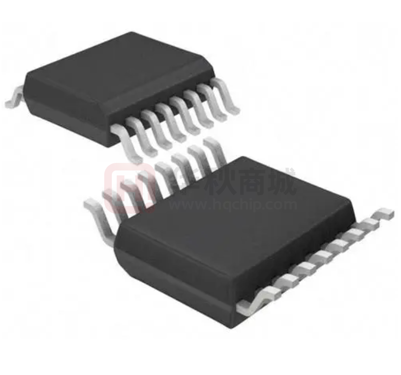
Package: 16-lead TSSOP
The SIG2012 is a low noise, low drift, and high-resolution 20-bit
analog-to-digital converter (ADC) with integrated programmable
gain amplifier (PGA) that offers high-accuracy measurement
solutions for bridge sensors.
The device contains a low noise PGA with gains selected from
128 or 256, a delta-sigma (Δ-Σ) modulator, and a SINC4 digital
filter. The output data rate from the device is fixed to 10SPS.
SPI-compatible interface is used for device configuration and
parity check is provided for data integrity.
The on-chip oscillator or an external clock can be used as the
clock source to the device.
The SIG2012 is available in 16-lead TSSOP package and is fully
specified over the -40°C to +125°C temperature range.
APPLICATIONS
Weigh Scales
Strain Gauges
Pressure Sensors
Industrial Process Control
Function Block Diagram
AVDD
TSSOP-16
DVDD
REFP REFN
BUF
Gain=128 or 256
AINP
AINN
PGA
ΔΣ ADC
Digital
Filter
Serial
Interface
Internal
Oscillator
AVSS GAIN
Sept. 2019
DVDD
1
16
DOUT/DRDYn
DGND
2
15
SCLK
CLKIN
3
14
DIN
NC
4
13
CSn
NC
5
12
AVDD
NC
6
11
AVSS
AINP
7
10
REFP
AINN
8
9
REFN
DOUT/DRDYn
SCLK
CLKIN
DGND
Signal Micro Incorporated
http://www.signal-micro.cn
SIG2012
TSSOP-16
�SIG2012
PIN CONFIGURATION and DESCRIPTIONS
TOP VIEW (Not To Scale)
PIN
DVDD
1
16
DOUT/DRDYn
DGND
2
15
SCLK
CLKIN
3
14
DIN
NC
4
13
CSn
NC
5
12
AVDD
NC
6
11
AVSS
AINP
7
10
REFP
AINN
8
9
REFN
FUNCTION
NO.
1
2
NAME
DVDD
DGND
3
CLKIN
Digital Input
4
GAIN
Digital Input
5
6
7
8
9
10
11
12
13
14
15
16
NC
NC
AINP
AINN
REFN
REFP
AVSS
AVDD
DGND
DVDD
SCLK
DOUT/DRDYn
Digital
Digital
Analog Input
Analog Input
Analog Input
Analog Input
Analog
Analog
Digital Input
Digital Input
Digital Input
Digital Output
Sept. 2019
Digital
Digital
SIG2012
TSSOP-16
DESCRIPTION
Digital power supply, 2.7V to 5.25V.
Digital ground reference point.
1) Internal oscillator: Connect to DGND.
2) External clock: Connect to external clock input.
PGA gain control:
DGND for gain=128 and DVDD for gain=256. Gain=128 if float.
No connection (float) or connect to DVDD/DGND.
No connection (float) or connect to DVDD/DGND.
Positive analog input.
Negative analog input.
Negative reference input.
Positive reference input.
Negative analog power supply.
Positive analog power supply. 2.7V to 5.25V relative to AVSS.
Connect to DGND or no connection (float).
Connect to DVDD or DGND.
Serial data clock.
Serial data output and data ready indicator.
Signal Micro Incorporated
http://www.signal-micro.cn
2
�SIG2012
PACKAGE/ORDERING INFORMATION
MODEL
PACKAGE DESCRIPTION
SPECIFIED TEMPERATURE
RANGE
ORDERING NUMBER
PACKING OPTION
SIG2012
TSSOP-16
-40°C to +125°C
SIG2012-ITSP16-RL
Reel, 5000
SPECIFICATIONS
Absolute Maximum Ratings
Over operating free-air temperature range, unless otherwise noted.(1)
Voltage
Current
Temperature
MIN
MAX
UNIT
AVDD to AVSS
–0.3
6.5
V
AVSS to DGND
–0.3
0.3
V
DVDD to DGND
–0.3
6.5
V
V
Analog input
VAVSS – 0.3
VAVDD + 0.3
Digital input
VDGND – 0.3
VDVDD + 0.3
V
Input current
–10
10
mA
Junction (TJ)
–50
150
°C
Storage (Tstg)
-60
150
°C
(1) Stresses beyond those listed under Absolute Maximum Ratings may cause permanent damage to the device. These is a stress rating only;
functional operation of the device at these or any other conditions above those indicated in the operational section of this specification is not
implied. Exposure to absolute maximum rating conditions for extended periods may affect device reliability.
ESD Ratings
SYMBOL
PARAMTER
CONDITION
VALUE
UNIT
HBM
Human-body model
ANSI/ESDA/JEDEC JS-001
±8000
V
MM
Machine model
JEDEC EIA/JESD22-A115C
±400
V
This integrated circuit can be damaged by ESD. Signal Micro recommends that all integrated circuits be handled with appropriate
precautions. Failure to observe proper handling and installation procedures can cause damage. ESD damage can range from
subtle performance degradation to complete device failure. Precision integrated circuits may be more susceptible to damage
because very small parametric changes could cause the device not to meet its published specifications.
Sept. 2019
Signal Micro Incorporated
http://www.signal-micro.cn
3
�SIG2012
Electrical Characteristics
Minimum/Maximum specifications apply from -40˚C to +125˚C. Typical specifications are at +25˚C. All specification are at
VAVDD=5V, VAVSS=0V, VDVDD=3.3V, VREF=5V, fCLK=1.2288MHz, data rate=10SPS, unless otherwise noted.
TEST CONDITION
OR NOTES
PARAMETER
MIN(1)
TYP
MAX(1)
UNITS
+VREF/Gain
VAVDD – 0.5
VAVDD – 0.5 –
|VINMAX|·Gain/2
V
V
ANALOG INPUTS
Differential Input Voltage
Absolute Input Voltage
VIN = VINP – VINN
–VREF/Gain
VAVSS + 0.5
VAVSS + 0.5 +
|VINMAX|·Gain/2
Common Mode Input Range
Absolute Input Current
V
1
nA
PGA Gain
128/256
V/V
Resolution
20
Bits
Data Rate
10
SPS
SYSTEM PERFORMANCE
Noise
See Noise Table 1
Integral Nonlinearity (INL)
±15
Offset Error
±2
μV
Offset Drift vs. Temperature
±10
nV/°C
Gain Error
±0.3
Gain Drift vs. Temperature
Normal Mode Rejection
(NMRR)
Common Mode Rejection
(CMRR)
(2)
Power Supply Rejection
(PSRR)
REFERENCE INPUT
Differential Reference Voltage
(VREF)
Absolute Negative Reference
Voltage (VREFN)
Absolute Positive Reference
Voltage (VREFP)
Average Voltage Input Current
2
ppm
%
5
ppm/°C
fIN=50/60Hz, ±2%,
100
110
dB
fIN=50/60Hz
100
120
dB
AVDD
75
90
dB
DVDD
80
120
dB
VREF = VREFP – VREFN
0.5
VAVDD – VAVSS + 0.1
V
VAVSS – 0.05
VREFP – 0.5
V
VREFN + 0.5
VAVDD + 0.05
V
20
nA
ADC CLOCK
External Clock
Internal Oscillator
Frequency Range
1
Duty Cycle
1.2288
40%
Nominal Frequency
1.25
1.2288
Accuracy
–3%
High-level Output Voltage (VOH)
IOH = 1mA
0.8·VDVDD
Low-level Output Voltage (VOL)
IOL = –1mA
MHz
60%
±0.5%
MHz
3%
DIGITAL INPUT/OUTPUT
V
0.2·VDVDD
V
High-level Input Voltage (VIH)
0.7·VDVDD
VDVDD
V
Low-level Input Voltage (VIL)
VDGND
0.3·VDVDD
V
Input Hysteresis
0.5
Input Leakage
V
±10
μA
POWER SUPPLY
AVSS Voltage (VAVSS)
0
V
AVDD Voltage (VAVDD)
2.7
5.25
V
DVDD Voltage (VDVDD)
2.7
5.25
V
0.65
0.9
mA
DVDD Current (IDVDD)
150
225
Total Power Dissipation
3.75
AVDD, AVSS Current (IAVDD)
Sept. 2019
Signal Micro Incorporated
http://www.signal-micro.cn
μA
mW
4
�SIG2012
TEMPERATURE RANGE
Specified temperature range
–40
125
°C
Operating temperature range
–50
125
°C
Storage temperature range
–60
150
°C
(1) Compliance to datasheet limits is assured by one or more methods: production test, characterization and/or design.
(2) Power supply rejection is specified DC change in voltage.
Sept. 2019
Signal Micro Incorporated
http://www.signal-micro.cn
5
�SIG2012
Timing Requirements: Serial Interface
Over the operating ambient temperature range and DVDD = 2.7V to 5.25V, unless otherwise noted.
B7
DOUT
B6
B5
B4
B3
B2
B1
B0
t2
t3
SCLK
t4
Figure 1. Serial Interface Timing Requirements
SYMBOL
t2
t3
t4
DESCRIPTION
SCLK rising edge to valid DOUT/DRDYn: propagation delay(1)
SCLK high pulse width
SCLK low pulse width
MIN
SCLK period
400
MAX
50
UNIT
ns
ns
ns
106
ns
200
200
(1) DOUT load = 20pF || 100k Ω to DGND.
Sept. 2019
Signal Micro Incorporated
http://www.signal-micro.cn
6
�SIG2012
NOISE PERFORMANCE
Table 1 and Table 2 show ADC noise performance in root mean square (RMS) value, peak-to-peak values, effective
number of bits (ENOB), and noise-free bits. The ENOB and noise-free bits listed in the tables are calculated using
Equation (1) and Equation (2):
ENOB= log 2 (2×VREF ⁄Gain⁄VRMS )
(1)
Noise Free Bits= log 2 �2×VREF ⁄Gain⁄Vp-p �
(2)
The noise data listed in the table are typical and are generated from continuous ADC readings with differential input
voltage of 0 V.
Table 1. ADC Noise in µVRMS (µVPP) at TA = 25°C, VAVDD = 5 V, VREF = 5 V
Gain
Data Rate
RMS Noise(nV)
Peak-to-Peak
Noise(nV)
ENOB(RMS)
Noise-Free Bits
128
10SPS
44
250
20.8
18.3
256
10SPS
44
250
19.8
17.3
Table 2. ADC Noise in µVRMS (µVPP) at TA = 25°C, VAVDD = 3 V, VREF = 3 V
Gain
Data Rate
RMS Noise(nV)
Peak-to-Peak
Noise(nV)
ENOB(RMS)
Noise-Free Bits
128
10SPS
44
250
20.1
17.6
256
10SPS
44
250
19.1
16.6
Sept. 2019
Signal Micro Incorporated
http://www.signal-micro.cn
7
�SIG2012
CIRCUIT DESCRIPTION
AVDD
DVDD
REFP REFN
BUF
Gain=128 or 256
AINP
AINN
PGA
ΔΣ ADC
Digital
Filter
Serial
Interface
SCLK
Internal
Oscillator
DGND
AVSS GAIN
Figure 2. SIG2012 Block Diagram
OVERVIEW
The SIG2012 is low noise, low drift, and high-resolution 20-bit analog-to-digital converter (ADC) with integrated
programmable gain amplifier (PGA). The ADC provides high-accuracy measurement solutions for bridge sensors.
Figure 2 shows the device block diagram.
The ADC features a high input-impedance, low-noise, programmable gain amplifier (PGA). The PGA gain is selectable
with 128 or 256 by GAIN input pin.
A delta-sigma modulator measures the PGA output voltage according to the buffered reference voltage to provide
high speed bitstream to the digital filter. Unlike SAR ADCs, this ADC is much easier to drive due to very high
impedance at both analog and reference inputs.
The digital filter provides SINC4 filter mode, allowing good line-cycle rejection. The date rate is fixed to 10SPS.
The SP-compatible serial interface is used to read the conversion data. The serial interface consists of two signals:
SCLK and DOUT/DRDYn. The DOUT/DRDYn pin serves as dual function of register and ADC data output and also
the indicator for data ready after the conversion is done. Parity check is provided for data integrity.
The ADC has two clock options: internal oscillator and external clock. The nominal clock frequency is 1.2288MHz.
The ADC operates with a single analog power supply with range from 2.7V to 5.25V. The digital power supply range
is 2.7 V to 5.25 V.
Sept. 2019
Signal Micro Incorporated
http://www.signal-micro.cn
8
�SIG2012
Programmable Gain Amplifier (PGA)
The ADC features a low-drift, low-noise, high input impedance programmable gain amplifier (PGA). The PGA input
is equipped with an electromagnetic-interference (EMI) filter consisting of two 350-Ω input resistors, and two 8pF
filter capacitors, as shown in the Figure 3.
350Ω
A1
8pF
ADC
A2
350Ω
8pF
Figure 3. Simplified PGA Block Diagram
The ADC full-scale voltage range is determined by the reference voltage and the PGA gain. Table 3 shows the fullscale voltage range verses gain for 5V reference voltage.
Table 3. ADC Full-Scale Voltage Range with VREF = 5V
FULL SCALE RANGE (V)(1)
±39 mV
±19.5 mV
GAIN
128
256
(1) The full scale input range is proportional to VREF.
Just like most amplifiers, there should be some headroom for the output of PGA to be away from the power supply
(VAVDD) and ground (VAVSS) due to the limitation of voltage driving capability of PGA output device as shown in Figure
4. For correct linear operation, the absolute PGA output voltage must locate within the range [VAVSS + 0.5, VAVDD –
0.5]. The analog input common voltage must meet Equation (3):
(VAVSS + 0.5 + VIN · Gain / 2) ≤ VCM ≤ (VAVDD – 0.5 – VIN · Gain / 2)
(3)
Where
VIN = differential input voltage = VINP – VINN
VCM = input common mode voltage = (VINP + VINN)/2
Sept. 2019
Signal Micro Incorporated
http://www.signal-micro.cn
9
�SIG2012
PGA Input
PGA Output
VAV DD
VAV DD – 0.5V
VOUTP = VCM+VIN ×Gain/2
VINP
VCM
VINN
VOUTN = VCM–VIN ×Gain/2
VAV SS + 0.5V
VAV SS
Figure 4. PGA Input and Output Range
Digital Filter and Conversion Time
A delta-sigma (Ʃ–Δ) ADC consists of a modulator followed by a programmable digital decimation filter to produce the
final high-resolution data output. Caution must be taken to choose the type of filtering based on the consideration of
tradeoffs between resolution, data rate, line cycle rejection, and conversion latency.
This ADC only provides sinc4 filter. Figure 5 shows the frequency response of the SINC4 and SINC1 filters normalized
to output data rate.
0
SINC1
SINC4
Amplitude (dB)
-20
-40
-60
-80
-100
-120
-140
-160
0
1
2
3
4
5
6
7
Normalized Frequency
8
9
10
Figure 5. Frequency Response of SINC1/SINC4 Filter
While the order of the SINC filter doesn’t affect the notch positions, the higher order SINC4 filter has wider notches
resulting in better rejection in the band (±1 Hz) around the notches. The higher order SINC4 filter also gives better
stop-band rejection with the tradeoff of longer settling time for the same output data rate. The SINC4 filter normally
takes four conversion cycles to settle, while SINC1 filter settles in one conversion cycle.
Clock Mode
The system clock of this ADC can be either from the internal oscillator or provided by external clock source to the
CLKIN pin. Figure 6 illustrates the configuration for each clock mode. If the CLKIN pin is shorted to analog ground
(AVSS), the internal oscillator is enabled. If an external clock is detected at the CLKIN pin, the ADC automatically
selects the external clock.
Sept. 2019
Signal Micro Incorporated
http://www.signal-micro.cn
10
�SIG2012
2.4576MHz
Clock
CLKIN
CLKIN
Option (a) : Internal Oscillator
Option (b): External Clock
Figure 6. Clock Mode Configurations
Power-On Reset (POR)
The ADC has two power supplies, analog and digital. The analog power supply (AVDD) range is 2.7V to 5V. The
digital supply (DVDD) range is 2.7V to 5V.
Figure 7 shows the POR sequence. The internal POR circuitry forces the ADC in reset state if the digital supply voltage
(VDVDD) is below POR voltage threshold which is about 1.3V. After the digital supply voltage (VDVDD) exceeds POR
voltage threshold, additional 54 ms of waiting time is needed for power supply to be fully settled before sending any
command, otherwise the command is ignored.
VDVDD
POR level: 1.3V typical
fCLK
Internal Reset
ADC Reset
ADC Normal Operation
54ms
Figure 7. Power-On Reset Sequence
SPI Interface
The ADC provides a 2-wire SPI-compatible interface with SPI Mode 1 supported. Please see Timing Requirements:
Serial Interface section for the timing information related to serial interface.
SERIAL CLOCK (SCLK)
The serial clock is a Schmitt-triggered input to make it noise immune. This pin is used to clock data into and out of the
device. Output data on DOUT pin are updated on the rising edge of SCLK.
DATA OUTPUT (DOUT/DRDYn)
The DOUT/DRDYn pin is a dual-function output. This pin serves as the serial interface data output and also as an
indicator for new data ready for retrieval. First, conversion or register data are shifted out on DOUT/DRDYn pin on the
rising edge of SCLK. Second, while the SPI interface is at idle state, the DOUT/DRDYn pin goes low to indicate that
new conversion data are ready for retrieval.
Data Format
The device provides 20 bits of conversion data output in binary 2’s complement format, left justified, MSB first. The
ADC input is bipolar-differential and is scaled such that zero differential input results in an ideal code of 20’h00000,
positive full scale input results in an ideal code of 20’h7FFFF, and negative full scale input results in an ideal code of
20’h80000. The output clips if the signal exceeds full-scale. Table 4 lists the ideal output codes for different input
signals.
Sept. 2019
Signal Micro Incorporated
http://www.signal-micro.cn
11
�SIG2012
Table 4. Ideal Output Code vs. Input Signal
INPUT SIGNAL
VIN = VINP – VINN
≥ FS (219 – 1) / 219
FS / 219
0
-FS / 219
≤ –FS
IDEAL OUTPUT
CODE
20’h7FFFF
20’h00001
20’h00000
20’hFFFFF
20’h80000
Reading ADC Data
As shown in Figure 8, the ADC data is 3 bytes long with 4-bit of LSB fixed to 4’b1111 after 20-bit conversion data,
DATA [19:0]. Parity byte is appended to the conversion data bytes after more than 24 SCLKs is applied. Part of parity
byte is formed by the checksum byte, which is the 8-bit sum of data conversion bytes plus an offset value, 8’h5B. The
first and last bit of parity byte are forced with 1’b1.
CHECKSUM [7:0] = DATA [19:12] + DATA [11:4] + {DATA [3:0], 4’b1111} + 8’h5B
PARITY [7:0] = {1’b1, CHECKSUM [6:1], 1’b1}
After four bytes are read, the data byte sequence is repeated when more SCLKs are sent. The repeating byte
sequence starts with the first byte DATA [19:12].
The read operation needs to complete 2 system clock cycles before the next new data is ready, otherwise the retrieved
data is corrupted by the updating of new data on DOUT/DRDYn pin.
1
9
21
17
25
8*n
33
SCLK
Data Ready
DOUT
New Data Ready
DATA[19:12]
DATA[11:4]
DATA[3:0]
4'b1111
PARITY[7:0]
DATA REPEAT
Optional
Figure 8. Reading Data Sequence
Sept. 2019
Signal Micro Incorporated
http://www.signal-micro.cn
12
�SIG2012
REVISION HISTORY
The revision history provided is for informational purposes only and is believed to be accurate, but not warranted.
Please go to web to make sure you have the latest revision.
DATE
REVISION
Jan. 20, 2019
May 15, 2019
Sept. 8, 2019
CHANGE
Initial release.
Add ordering information.
Add pin 4 GAIN description for float condition.
DISCLAIMER
Signal Micro reserves the right to make any change in circuit design, specification or other related things if necessary
without notice at any time.
All trademarks and registered trademarks are the property of their respective owners.
Sept. 2019
Signal Micro Incorporated
http://www.signal-micro.cn
13
�SIG2012
PACKAGE OUTLINE DIMENSIONS
0.30
0.19
0.65
16
0.10
M
9
0.15 NOM
4.50
4.30
6.60
6.20
0.25
0o-8o
0.75
0.50
8
1
5.10
4.90
1.10 MAX
0.15
0.05
0.10
Seating Plane
A. Compliant to JEDEC STARDARDS MO-153-AD.
B. All linear dimensions are in millimeters.
C. This drawing is subject to change without notice.
Sept. 2019
Signal Micro Incorporated
http://www.signal-micro.cn
14
�


 工商网监
湘ICP备2023018690号
工商网监
湘ICP备2023018690号
