SIG7190
SIG7190: 4.8kSPS, 24-bit Sigma-Delta ADC with PGA
FEATURES
DESCRIPTION
Programmable Gain: 1/2/4/8/16/32/64/128
Data Rates: 4.7SPS to 4.8kSPS
RMS Noise: 15nV at 10SPS (Gain=128)
22.4 noise-free bits at 10SPS (Gain=1)
Offset Drift: 3nV/°C (Gain=128)
Gain Drift: 0.5ppm/°C
Integral Non-Linearity: 2ppm
Internal or External Clock
Simultaneous 50Hz/60Hz Rejection
2 Differential/4 Pseudo Differential Inputs
Automatic Channel Sequencer
Burnout Current Sources
4 General Purpose Digital Outputs
Parity Check
Power Supply
AVDD: 2.7V to 5.25V or ±2.5V
DVDD: 2.7V to 5.25V
Current: 2.7mA
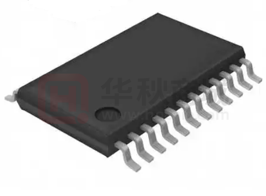
Package: 24-lead TSSOP
The SIG7190 is a low noise, low drift, and high-resolution 24-bit
analog-to-digital converter (ADC) with integrated programmable
gain amplifier (PGA) that offers high-accuracy measurement
solutions for bridge sensors, thermocouples, and resistance
temperature devices (RTD).
The device contains a low noise PGA with gains selected from
1, 2, 4, 8 16, 32, 64, and 128, a delta-sigma (Δ-Σ) modulator,
and a programmable digital SINC4/SINC3/fast settling filter.
50Hz/60Hz simultaneous rejection option is also provided. The
output data rate from the device can be configured from 4.7SPS
up to 4800SPS. This device provides channel sequencer feature
to measure two differential inputs or four pseudo differential
inputs automatically. Burnout current sources are provided at the
analog inputs for sensor connection diagnosis.
Offset and gain calibration registers are provided with calibration
command or direct register write to calibrate the ADC errors or
overall system errors. SPI-compatible interface is used for
device configuration and parity check is provided for data
integrity.
The on-chip oscillator, an external clock, or an external crystal
can be used as the clock source to the device.
The device can operate with bipolar ±1.35V to ±2.625V analog
power supplies, or with a single 2.7V to 5.25V analog power
supply.
APPLICATIONS
The SIG7190 is available in 24-lead TSSOP package and is fully
specified over the -40°C to +125°C temperature range.
Weigh Scales
Strain Gauges
Temperature Measurement
Industrial Process Control
Pressure Sensors
TSSOP-24
Function Block Diagram
AVDD
DVDD
REFIN1+ REFIN1-
MCLK1
1
24
MCLK2
2
23
DOUT/DRDYn
SCLK
3
22
SYNCn_PDn
CS
4
21
DVDD
P3
5
20
AVDD
P2
6
19
DGND
P1/REFIN2+
7
18
AGND
P0/REFIN2-
8
17
BPDSW
NC
9
16
REFIN1-
AINCOM 10
15
REFIN1+
AIN1 11
14
AIN4
AIN2 12
13
AIN3
REFERENCE
DETECT
Gain=1,2,4,8,
16,32,64.128
BUF
AIN4
MUX
AIN1
AIN2
AIN3
PGA
SYNCn_PDn
CSn
ΔΣ ADC
Digital
Filter
Serial
Interface
And
Control
Logic
AINCOM
DOUT/DRDYn
SCLK
P3
P2
TEMP
Sensor
BPDSW
AGND
Sept. 2021
DIN
Internal
Oscillator
P0/REFIN2- P1/REFIN2+
Clock
Circuitry
MCLK2
SIG7190
TSSOP-24
DIN
MCLK1
DGND
Signal Micro Incorporated
http://www.signal-micro.cn
�SIG7190
PIN CONFIGURATION and DESCRIPTIONS
TOP VIEW (Not To Scale)
PIN
MCLK1
1
24
MCLK2
2
23
DOUT/DRDYn
SCLK
3
22
SYNCn_PDn
CS
4
21
DVDD
P3
5
20
AVDD
P2
6
19
DGND
P1/REFIN2+
7
18
AGND
P0/REFIN2-
8
17
BPDSW
NC
SIG7190
TSSOP-24
DIN
9
16
REFIN1-
AINCOM 10
15
REFIN1+
AIN1 11
14
AIN4
AIN2 12
13
AIN3
FUNCTION
DESCRIPTION
SCLK
Digital Input
Digital
Input/Output
Digital Input
Crystal Connection.
Master clock input or internal clock output depending on MODE Register
bits CLK[1:0].
Serial data clock.
4
5
CSn
P3
Digital Input
Analog Output
Serial chip select. Active low.
General purpose output bit between AVDD and AGND.
6
P2
7
P1/REFIN2+
8
P0/REFIN2-
9
10
NC
AINCOM
Analog Output
Analog
Input/Output
Analog
Input/Output
Analog
Analog Input
General purpose output bit between AVDD and AGND.
General purpose output bit between AVDD and AGND or second
positive reference input.
General purpose output bit between AVDD and AGND or second
negative reference input.
No connection (float) or connect to AVDD/AGND.
Negative analog input for pseudo differential operation.
11
12
AIN1
AIN2
Analog Input
Analog Input
Analog input channel 1.
Analog input channel 2.
13
14
AIN3
AIN4
Analog Input
Analog Input
Analog input channel 3.
Analog input channel 4.
15
16
REFIN1+
REFIN1-
Analog Input
Analog Input
Positive reference input.
Negative reference input.
17
BPDSW
Analog Input
18
AGND
Analog
19
DGND
Digital
20
AVDD
Analog
21
DVDD
Digital
22
SYNCn_PDn
Digital Input
23
24
DOUT/DRDYn
DIN
Digital Output
Digital Input
Bridge Power-down switch to AGND.
Negative analog power supply. AGND can be taken below DVSS to
provide bipolar power supplies. For example, AGND can be tied to –
2.5V and AVDD can be tied to +2.5V, providing a ±2.5V dual supplies
to the ADC.
Digital ground reference point.
Positive analog power supply. 2.7V to 5.25V relative to AGND. AVDD
is independent of DVDD.
Digital power supply, 2.7V to 5.25V. DVDD is independent of AVDD.
Synchronization control signal. While this pin is low, the digital filter is
reset and DOUT pin is forced to high. The device starts a new
conversion after this pin goes back to high. The device enters powerdown if holding this pin low for longer than 0.83ms.
Serial data output and data ready indicator.
Serial data input.
NO.
NAME
1
MCLK1
2
MCLK2
3
Sept. 2021
Signal Micro Incorporated
http://www.signal-micro.cn
2
�SIG7190
PACKAGE/ORDERING INFORMATION
MODEL
PACKAGE DESCRIPTION
SPECIFIED TEMPERATURE
RANGE
ORDERING NUMBER
PACKING OPTION
SIG7190
TSSOP-24
-40°C to +125°C
SIG7190-ITSP24-RL
Reel, 3000
SPECIFICATIONS
Absolute Maximum Ratings
Over operating free-air temperature range, unless otherwise noted.(1)
Voltage
Current
Temperature
MIN
MAX
UNIT
AVDD to AGND
–0.3
6.5
V
AGND to DGND
–3
0.3
V
DVDD to DGND
–0.3
6.5
V
V
Analog input
VAGND – 0.3
VAVDD + 0.3
Digital input
VDGND – 0.3
VDVDD + 0.3
V
Input current
–10
10
mA
Junction (TJ)
–50
150
°C
Storage (Tstg)
-60
150
°C
(1) Stresses beyond those listed under Absolute Maximum Ratings may cause permanent damage to the device. These is a stress rating only;
functional operation of the device at these or any other conditions above those indicated in the operational section of this specification is not
implied. Exposure to absolute maximum rating conditions for extended periods may affect device reliability.
ESD Ratings
SYMBOL
PARAMTER
CONDITION
VALUE
UNIT
HBM
Human-body model
ANSI/ESDA/JEDEC JS-001
±8000
V
CDM
Charged-device model
JEDEC EIA/JESD22-C101F
±2000
V
MM
Machine model
JEDEC EIA/JESD22-A115C
±600
V
This integrated circuit can be damaged by ESD. Signal Micro recommends that all integrated circuits be handled with appropriate
precautions. Failure to observe proper handling and installation procedures can cause damage. ESD damage can range from
subtle performance degradation to complete device failure. Precision integrated circuits may be more susceptible to damage
because very small parametric changes could cause the device not to meet its published specifications.
Sept. 2021
Signal Micro Incorporated
http://www.signal-micro.cn
3
�SIG7190
Electrical Characteristics
Minimum/Maximum specifications apply from -40˚C to +125˚C. Typical specifications are at +25˚C. All specification are at
VAVDD=5V, VAGND=0V, VDVDD=3.3V, VREF=2.5V, fCLK=4.9152MHz, data rate=10SPS, and PGA Gain=1, unless otherwise noted.
PARAMETER
TEST CONDITION
OR NOTES
MIN(1)
MAX(1)
UNITS
–VREF/Gain
+VREF/Gain
V
VAGND – 0.05
VAGND + 0.5
VAGND + 0.5 +
|VINMAX|·Gain/2
VAVDD + 0.05
VAVDD – 0.5
VAVDD – 0.5 –
|VINMAX|·Gain/2
TYP
ANALOG INPUTS
Differential Input Voltage
VIN = VINP – VINN
Absolute Input Voltage
Buffer Off, Gain=1
Buffer On
Common Mode Input Range
Buffer On
Absolute Input Current
Buffer off, Gain=1
Buffer On
±100
±2
V
V
nA
nA
SYSTEM PERFORMANCE
PGA Gain
1/2/4/8/16/32/64/128
V/V
Resolution
24
Bits
Data Rate
4.7
Noise
Integral Nonlinearity (INL)
4800
SPS
See Noise Table
Buffer Off, Gain=1
Buffer On
±10
ppm
±2
ppm
Offset Error
All PGA gains
±150/Gain
μV
Offset Drift vs. Temperature
All PGA gains
±150/Gain ± 2
nV/°C
-0.0025
±0.001
Gain Error(2)
Gain = 8, 16, and 32
-0.01
±0.004
-0.01
Gain = 64 and 128
-0.025
±0.01
-0.025
-3
±0.5
+3
Gain = 1, 2, and 4
Gain Drift vs. Temperature
Normal Mode Rejection
(NMRR)
Common Mode Rejection
(CMRR)
Power Supply Rejection(2)
(PSRR)
REFERENCE INPUT
Differential Reference Voltage
(VREF)
Absolute Negative Reference
Voltage (VREFN)
Absolute Positive Reference
Voltage (VREFP)
Average Voltage Input Current
All PGA gains
fIN = 50/60Hz, ±2%,
data rate=10SPS
fIN = 50Hz,
data rate = 1200SPS
AVDD, AGND
-0.0025
%
ppm/°C
See Table 20
dB
100
120
dB
85
105
dB
DVDD
90
110
dB
VREF = VREFP – VREFN
0.5
VAVDD – VAGND + 0.1
V
VAGND – 0.05
VREFP – 0.5
V
VREFN + 0.5
VAVDD + 0.05
V
±500
nA
500
nA
Burnout Current Sources
Current Setting
ADC CLOCK
External Clock
Internal Oscillator
Crystal Oscillation
Frequency Range
Duty Cycle
1
40%
Nominal Frequency
Accuracy
Frequency Range
4.9152
5.0
60%
4.9152
MHz
–3%
±0.5%
3%
1
4.9152
2.5
Start-up time
MHz
20
MHz
ms
DIGITAL INPUT/OUTPUT
High-level Output Voltage (VOH)
IOH = 4mA
Low-level Output Voltage (VOL)
IOL = –4mA
0.8·VDVDD
V
0.2·VDVDD
V
High-level Input Voltage (VIH)
0.7·VDVDD
VDVDD
V
Low-level Input Voltage (VIL)
VDGND
0.3·VDVDD
V
Sept. 2021
Signal Micro Incorporated
http://www.signal-micro.cn
4
�SIG7190
Input Hysteresis
0.5
V
Input Leakage
±10
μA
POWER SUPPLY
AGND Voltage (VAGND)
–2.625
0
V
AVDD Voltage (VAVDD)
VAGND + 2.7
VAGND + 5.25
V
DVDD Voltage (VDVDD)
2.7
5.25
V
AVDD, AGND Current (IAVDD)
DVDD Current (IDVDD)
Total Power Dissipation
Buffer Off
0.9
1.3
mA
Buffer On
2.5
3.2
mA
Sleep Mode
1
μA
Power-down Mode
1
μA
360
μA
Active Mode
260
Sleep Mode
50
μA
Power-down Mode
1
μA
Buffer Off
5.5
mW
Buffer On
13.5
mW
Sleep Mode
0.16
mW
Power-down Mode
0.01
mW
TEMPERATURE RANGE
Specified temperature range
–40
125
°C
Operating temperature range
–50
125
°C
Storage temperature range
–60
150
°C
(1) Compliance to datasheet limits is assured by one or more methods: production test, characterization and/or design.
(2) MIN and MAX values listed for gain error are for +25˚C room temperature only.
Sept. 2021
Signal Micro Incorporated
http://www.signal-micro.cn
5
�SIG7190
Timing Requirements: Serial Interface
Over the operating ambient temperature range and DVDD = 2.7V to 5.25V, unless otherwise noted.
t7
CSn
t6
t1
t5
B7
DOUT
B6
B5
B4
B3
B2
B1
B0
t2
t8
t3
SCLK
t4
t9
t10
DIN
B7
B6
B5
B4
B3
B2
B1
B0
Figure 1. Serial Interface Timing Requirements
SYMBOL
t1
t2
t3
t4
DESCRIPTION
CSn falling edge to DOUT/DRDYn driven: propagation delay(1)
SCLK falling edge to valid DOUT/DRDYn: propagation delay(1)
SCLK low pulse width
MIN
SCLK high pulse width
100
SCLK period
MAX
50
50
100
200
UNIT
ns
ns
ns
ns
106
ns
40
ns
t5
CSn rising edge to DOUT high impedance: propagation delay
t6
Last SCLK rising edge to CSn rising edge: delay time
50
ns
t7
CSn high pulse width
50
ns
50
ns
time(2)
t8
CSn falling edge to first SCLK falling edge: setup
t9
Valid DIN to SCLK rising edge: setup time
50
ns
t10
Valid DIN to SCLK rising edge: hold time
25
ns
(1) DOUT load = 20pF || 100k Ω to DGND.
(2) CSn can be tied low.
Sept. 2021
Signal Micro Incorporated
http://www.signal-micro.cn
6
�SIG7190
NOISE PERFORMANCE
The noise performance of the ADC is affected by PGA gain, data rate, and digital filter setting. The following tables
show the rms noise and peak-to-peak noise for SINC4 and SINC3 filters and fast settling mode with chop disabled.
The effective number of bits (ENOB) and noise-free bits are also listed according to Equation (1) and Equation (2):
ENOB= log 2 (2×VREF ⁄Gain⁄VRMS )
(1)
Noise Free Bits= log 2 �2×VREF ⁄Gain⁄Vp-p �
(2)
The noise data listed in the table are typical and are generated from continuous ADC readings with differential input
voltage of 0 V. With chop enabled, the resolution improves by 0.5 bits.
SINC4 and Chop Disabled
Table 1. ADC Noise in µVRMS (µVPP) at TA = 25°C, VAVDD = 5 V, VREF = 5 V, SINC4 Filter, Chop Disabled
Filter
Word
Data
Rate
(SPS)
1023
640
480
96
80
32
16
5
2
1
4.7
7.5
10
50
60
150
300
960
2400
4800
PGA GAIN
1
2
4
8
16
32
64
128
0.211(1.27)
0.267(1.60)
0.308(1.85)
0.689(4.13)
0.755(4.52)
1.19(7.15)
1.64(8.94)
2.69(17.9)
6.91(55.4)
57.8(427)
0.126(0.686)
0.159(0.866)
0.183(1.00)
0.410(2.24)
0.449(2.45)
0.710(3.87)
0.940(5.36)
1.80(11.9)
3.89(30.7)
29.1(229)
0.069(0.368)
0.087(0.465)
0.101(0.537)
0.225(1.20)
0.247(1.32)
0.390(2.08)
0.574(3.13)
1.10(6.86)
2.17(15.6)
14.4(153)
0.044(0.264)
0.055(0.333)
0.064(0.385)
0.143(0.860)
0.157(0.942)
0.248(1.49)
0.353(1.79)
0.652(4.02)
1.20(9.16)
7.36(61.5)
0.028(0.138)
0.035(0.175)
0.041(0.202)
0.091(0.451)
0.099(0.495)
0.157(0.782)
0.213(1.19)
0.391(2.31)
0.691(4.99)
3.60(30.6)
0.018(0.099)
0.023(0.125)
0.027(0.144)
0.059(0.323)
0.065(0.354)
0.103(0.559)
0.143(0.708)
0.269(1.68)
0.434(3.07)
1.86(15.4)
0.013(0.073)
0.017(0.092)
0.019(0.106)
0.043(0.237)
0.047(0.259)
0.075(0.410)
0.109(0.671)
0.191(1.24)
0.310(2.30)
0.969(7.14)
0.010(0.054)
0.013(0.069)
0.015(0.079)
0.033(0.177)
0.036(0.194)
0.057(0.307)
0.086(0.494)
0.148(0.955)
0.242(1.63)
0.557(4.00)
Table 2. ADC ENOB (Noise Free Bits) at TA = 25°C, VAVDD = 5 V, VREF = 5 V, SINC4 Filter, Chop Disabled
Filter
Word
Data
Rate
(SPS)
1023
640
480
96
80
32
16
5
2
1
4.7
7.5
10
50
60
150
300
960
2400
4800
Sept. 2021
PGA GAIN
1
2
4
8
16
32
64
128
25.5(22.9)
25.2(22.6)
25.0(22.4)
23.8(21.2)
23.7(21.1)
23.0(20.4)
22.5(20.1)
21.8(19.1)
20.5(17.5)
17.4(14.5)
25.2(22.8)
24.9(22.5)
24.7(22.3)
23.5(21.1)
23.4(21.0)
22.7(20.3)
22.3(19.8)
21.4(18.7)
20.3(17.3)
17.4(14.4)
25.1(22.7)
24.8(22.4)
24.6(22.1)
23.4(21.0)
23.3(20.9)
22.6(20.2)
22.1(19.6)
21.1(18.5)
20.1(17.3)
17.4(14.0)
24.8(22.2)
24.4(21.8)
24.2(21.6)
23.1(20.5)
22.9(20.3)
22.3(19.7)
21.8(19.4)
20.9(18.2)
20.0(17.1)
17.4(14.3)
24.4(22.1)
24.1(21.8)
23.9(21.6)
22.7(20.4)
22.6(20.3)
21.9(19.6)
21.5(19.0)
20.6(18.0)
19.8(16.9)
17.4(14.3)
24.0(21.6)
23.7(21.3)
23.5(21.0)
22.3(19.9)
22.2(19.8)
21.5(19.1)
21.1(18.8)
20.1(17.5)
19.5(16.6)
17.4(14.3)
23.5(21.0)
23.2(20.7)
22.9(20.5)
21.8(19.3)
21.7(19.2)
21.0(18.5)
20.5(17.8)
19.6(16.9)
18.9(16.1)
17.3(14.4)
22.9(20.5)
22.5(20.1)
22.3(19.9)
21.2(18.7)
21.0(18.6)
20.4(18.0)
19.8(17.3)
19.0(16.3)
18.3(15.6)
17.1(14.3)
Signal Micro Incorporated
http://www.signal-micro.cn
7
�SIG7190
SINC3 and Chop Disabled
Table 3. ADC Noise in µVRMS (µVPP) at TA = 25°C, VAVDD = 5 V, VREF = 5 V, SINC3 Filter, Chop Disabled
Filter
Word
Data
Rate
(SPS)
1023
640
480
96
80
32
16
5
2
1
4.7
7.5
10
50
60
150
300
960
2400
4800
PGA GAIN
1
2
4
8
16
32
64
128
0.229(1.37)
0.289(1.73)
0.334(2.00)
0.747(4.46)
0.818(4.89)
1.29(7.73)
1.70(10.1)
5.26(32.8)
67.0(351)
558(3050)
0.139(0.844)
0.175(1.07)
0.202(1.23)
0.453(2.75)
0.496(3.02)
0.784(4.77)
1.08(6.56)
3.01(19.1)
35.5(184)
277(1530)
0.080(0.447)
0.101(0.565)
0.117(0.652)
0.262(1.46)
0.287(1.60)
0.453(2.53)
0.666(3.87)
1.67(10.6)
17.3(96.7)
138(787)
0.047(0.303)
0.060(0.382)
0.069(0.441)
0.154(0.987)
0.169(1.08)
0.267(1.71)
0.372(2.38)
0.889(5.51)
8.81(51.3)
68.8(393)
0.032(0.158)
0.041(0.200)
0.047(0.231)
0.105(0.516)
0.115(0.565)
0.182(0.894)
0.226(1.34)
0.516(3.95)
4.30(24.2)
34.7(185)
0.019(0.122)
0.023(0.154)
0.027(0.178)
0.061(0.398)
0.066(0.436)
0.105(0.689)
0.153(0.931)
0.310(1.86)
2.18(13.6)
17.8(98.3)
0.014(0.087)
0.018(0.110)
0.021(0.127)
0.047(0.284)
0.051(0.311)
0.081(0.492)
0.117(0.687)
0.207(1.44)
1.10(6.42)
8.65(48.4)
0.011(0.064)
0.014(0.081)
0.017(0.093)
0.037(0.209)
0.040(0.229)
0.064(0.362)
0.097(0.540)
0.165(1.03)
0.592(3.72)
4.37(25.0)
Table 4. ADC ENOB (Noise Free Bits) at TA = 25°C, VAVDD = 5 V, VREF = 5 V, SINC3 Filter, Chop Disabled
Filter
Word
Data
Rate
(SPS)
1023
640
480
96
80
32
16
5
2
1
4.7
7.5
10
50
60
150
300
960
2400
4800
PGA GAIN
1
2
4
8
16
32
64
128
25.4(22.8)
25.0(22.5)
24.8(22.3)
23.7(21.1)
23.5(21.0)
22.9(20.3)
22.5(19.9)
20.9(18.2)
17.2(14.8)
14.1(11.7)
25.1(22.5)
24.8(22.2)
24.6(22.0)
23.4(20.8)
23.3(20.7)
22.6(20.0)
22.1(19.5)
20.7(18.0)
17.1(14.7)
14.1(11.7)
24.9(22.4)
24.6(22.1)
24.3(21.9)
23.2(20.7)
23.1(20.6)
22.4(19.9)
21.8(19.3)
20.5(17.9)
17.1(14.7)
14.1(11.6)
24.7(22.0)
24.3(21.6)
24.1(21.4)
23.0(20.3)
22.8(20.1)
22.2(19.5)
21.7(19.0)
20.4(17.8)
17.1(14.6)
14.1(11.6)
24.2(21.9)
23.9(21.6)
23.7(21.4)
22.5(20.2)
22.4(20.1)
21.7(19.4)
21.4(18.8)
20.2(17.3)
17.1(14.7)
14.1(11.7)
24.0(21.3)
23.7(21.0)
23.5(20.7)
22.3(19.6)
22.2(19.5)
21.5(18.8)
21.0(18.4)
19.9(17.4)
17.1(14.5)
14.1(11.6)
23.4(20.8)
23.0(20.4)
22.8(20.2)
21.7(19.1)
21.5(18.9)
20.9(18.3)
20.3(17.8)
19.5(16.7)
17.1(14.6)
14.1(11.7)
22.7(20.2)
22.4(19.9)
22.2(19.7)
21.0(18.5)
20.9(18.4)
20.2(17.7)
19.6(17.1)
18.9(16.2)
17.0(14.4)
14.1(11.6)
Fast Settling, Average=16, SINC4 and Chop Disabled
Table 5. ADC Noise in µVRMS (µVPP) at TA = 25°C, VAVDD = 5 V, VREF = 5 V, SINC4 Filter, Chop Disabled
Filter
Word
Data
Rate
(SPS)
96
30
6
5
2
1
3.125
10
50
60
150
300
PGA GAIN
1
2
4
8
16
32
64
128
0.286(1.36)
0.511(2.43)
1.14(5.44)
1.25(5.96)
1.61(7.75)
3.73(22.7)
0.144(0.816)
0.258(1.46)
0.578(3.26)
0.633(3.58)
0.927(5.36)
2.05(11.6)
0.080(0.442)
0.143(0.791)
0.320(1.77)
0.351(1.94)
0.595(3.73)
1.18(7.60)
0.042(0.221)
0.076(0.396)
0.170(0.885)
0.186(0.969)
0.359(1.86)
0.587(3.28)
0.030(0.144)
0.053(0.258)
0.120(0.578)
0.131(0.633)
0.218(1.04)
0.340(1.94)
0.020(0.098)
0.036(0.175)
0.081(0.391)
0.089(0.428)
0.135(0.689)
0.228(1.34)
0.015(0.076)
0.027(0.137)
0.061(0.306)
0.067(0.335)
0.107(0.596)
0.155(0.903)
0.012(0.062)
0.021(0.110)
0.047(0.246)
0.051(0.270)
0.089(0.442)
0.113(0.666)
Table 6. ADC ENOB (Noise Free Bits) at TA = 25°C, VAVDD = 5 V, VREF = 5 V, SINC4 Filter, Chop Disabled
Filter
Word
Data
Rate
(SPS)
96
30
6
5
2
1
3.125
10
50
60
150
300
Sept. 2021
PGA GAIN
1
2
4
8
16
32
64
128
25.1(22.8)
24.2(22.0)
23.1(20.8)
22.9(20.7)
22.6(20.3)
21.4(18.8)
25.0(22.5)
24.2(21.7)
23.0(20.5)
22.9(20.4)
22.4(19.8)
21.2(18.7)
24.9(22.4)
24.1(21.6)
22.9(20.4)
22.8(20.3)
22.0(19.4)
21.0(18.3)
24.8(22.4)
24.0(21.6)
22.8(20.4)
22.7(20.3)
21.7(19.4)
21.0(18.5)
24.3(22.0)
23.5(21.2)
22.3(20.0)
22.2(19.9)
21.5(19.2)
20.8(18.3)
23.9(21.6)
23.0(20.8)
21.9(19.6)
21.7(19.5)
21.1(18.8)
20.4(17.8)
23.3(21.0)
22.4(20.1)
21.3(19.0)
21.2(18.8)
20.5(18.0)
19.9(17.4)
22.7(20.3)
21.8(19.4)
20.7(18.3)
20.5(18.1)
19.7(17.4)
19.4(16.8)
Signal Micro Incorporated
http://www.signal-micro.cn
8
�SIG7190
ON-CHIP REGISTER MAPS
There are total eight registers inside the device which is 8-bit or 24-bit wide. These registers are used to configure and
control the ADC to the desired mode of operation. These registers can be accessed through the SPI-compatible serial
interface by using register read and write commands. At power-on or reset, the registers default to their initial settings,
as shown in the Reset Value column of Table 7.
Table 7. Register map
BIT 7
BIT 6
BIT 5
R
RESET
VALUE
80
DRDYn
NOREF
MODE
R/W
080060
SINC3
ERR
MD[2:0]
0
CHOP
0
0
CONFIG
R/W
000117
BCS
REFDET
0
x
0
x
BPDSW
x
GP32EN
ADDR.
NAME
DIR.
3’b000
STATUS
3’b001
3’b010
3’b011
DATA
R
000000
3’b100
3’b101
ID
GPOCON
R
R/W
X0
00
3’b110
OFFSET
R/W
800000
3’b111
GAIN
R/W
555555
ENPAR
BIT 4
BIT 3
BIT 2
BIT 1
BIT 0
PARITY
CHD[3:0]
DATUS
CLK[1:0]
AVG[1:0]
0
SINGLE
REJ60
FS[9:8]
FS[7:0]
REFSEL
0
0
0
0
CH[7:0]
BUF
FORMAT
PGA[2:0]
DATA[23:16]
DATA[15:8]
DATA[7:0]
x
0
0
0
0
GP10EN
P3DAT
P2DAT
P1DAT
P0DAT
OFFSET[23:16]
OFFSET[15:8]
OFFSET[7:0]
GAIN[23:16]
GAIN[15:8]
GAIN[7:0]
STATUS Register
Table 8. STATUS Register (Address = 3’b000)
BIT 7
BIT 6
BIT 5
BIT 4
DRDYn
ERR
NOREF
PARITY
BIT 3
BIT 2
BIT 1
BIT 0
CHD[3:0]
Power-On/Reset Value = 0x80
Bits
Bit Name
Access
Reset
Description
7
DRDYn
R
1’b1
ADC Ready Bit: This bit is cleared when new data is written to the
ADC data register. It is set automatically after the ADC data register is
read. In addition to this bit, DOUT/DRDYn pin can also be used as an
alternative to monitor the update of new ADC data.
6
ERR
R
1’b0
ADC Error Bit. This bit is written at the same time as new data
update. Error sources include input overrange, input underrange, or
lower than expected reference voltage.
5
NOREF
R
1’b0
No External Reference Bit: The function of this bit is only enabled by
setting the REFDET bit in the CONFIG Register to 1. While the
REFDET bit is 1 and the selected reference voltage is below a
specified threshold, which is about 0.4V, this bit is set and conversion
results are clamped to all 1s.
4
PARITY
R
1’b0
Parity Check Bit: The function of this bit is only enabled by setting the
ENPAR bit in
MODE Register to 1. While the ENPAR bit is 1 and there is odd
number of 1s in the data register, this bit is set. Otherwise it is always
0.
3:0
CHD[3:0]
R
4’b0000
Data Channel Number: These bits indicate the corresponding
channel to the ADC data in data register (see Table 11).
Sept. 2021
Signal Micro Incorporated
http://www.signal-micro.cn
9
�SIG7190
MODE Register
Table 9. MODE Register (Address = 3’b001)
BIT 23
BIT 22
BIT 21
BIT 20
BIT 19
BIT18
BIT 17
BIT 16
BIT 15
BIT 14
BIT 13
BIT 12
BIT 11
BIT10
BIT 9
BIT 8
BIT 6
BIT 5
BIT 4
BIT 3
BIT 2
BIT 1
BIT 7
MD[2:0]
SINC3
DATUS
0
ENPAR
CLK[1:0]
0
SINGLE
BIT 0
AVG[1:0]
REJ60
FS[9:8]
FS[7:0]
Power-On/Reset Value = 0x080060
Bits
Bit Name
Access
Reset
Description
23:21
MD[2:0]
R/W
3’b000
Mode Select Bits: These bits select the operating mode of the device.
000: Continuous conversion mode. (default)
001: Single conversion mode. ADC first wakeup if in idle or sleep
mode; resets the filter to perform one conversion; and enters sleep
mode. The conversion result remains in the data register with
DOUT/DRDYn as low.
010: Idle mode. The digital filter is in reset state with ADC free running.
011: Sleep mode. Most of circuitry is turned off to save the power.
BPDSW remains active in sleep mode.
100: Internal zero-scale calibration.
101: Internal full-scale calibration.
110: System zero-scale calibration.
111: System full-scale calibration.
For each above calibration mode, DOUT/DRDYn goes high when the
calibration is initiated and returns low when the calibration is complete.
The ADC is automatically placed in idle mode after the calibration. The
measured offset/full-scale coefficient is placed in the offset/full-scale
register of the selected channel.
20
DATUS
R/W
1’b0
Status Enable Bit: When DATUS is set, the contents of the status
register are transmitted along with each data register read.
19:18
CLK[1:0]
R/W
2’b10
Clock Select Bits: This bits select the clock source for SYSCLK.
00: External crystal applied between MCLK1 and MCLK2.
01: External clock applied to the MCLK2 pin.
10: Internal 4.9152MHz clock with MCLK2 tristated. (default)
11: Internal 4.9152MHz clock with its output on MCLK2 pin.
17:16
AVG[1:0]
R/W
2’b00
Fast Settling Filter Setting: In fast settling mode, a first-order
average is added after the SINC filter to further improve the rms noise.
It can work for any data rate select bits FS[9:0].
00: Not averaging (default)
01: Average by 2
10: Average by 8
11: Average by 16
15
SINC3
R/W
1’b0
SINC3 Enable Bit:
0: SINC4 filter (default)
1: SINC3 filter
14
RESERVED
R/W
1’b0
Reserved
Always write 1’b0
13
ENPAR
R/W
1’b0
Enable Parity Bit: This bit enables the parity check on the data
register.
12
RESERVED
R/W
1’b0
Reserved
Always write 1’b0
Sept. 2021
Signal Micro Incorporated
http://www.signal-micro.cn
10
�SIG7190
11
SINGLE
R/W
1’b0
Single Cycle Conversion Bit: When this bit is set, the ADC settles in
one conversion cycle so that it functions as a zero latency ADC. When
chop is disabled, fast settling mode is disabled, continuous conversion
mode is selected, and SINGLE bit is set, the output data rate is
Output Data Rate=SYSCLK/1024/FS[9:0]/N
Where N is 3 for SINC3 filter and 4 for SINC4 filter. With a nominal
SYSCLK of 4.9152MHz, default Data Rate bits 0x060=96, and SINC3
bit set to 0, output data rate is 4915200/1024/96/4=12.5SPS.
10
REJ60
R/W
1’b0
50/60Hz Notch Bit: This bit can only be effective while FS[9:0]=0x060.
A filter notch is placed at 60Hz to allow simultaneous 50Hz/60Hz
rejection.
9:0
FS[9:0]
R/W
0x060
Data Rate Select Bits: The 10 bits are used to configure the ADC
data rate. When chop is disabled, fast settling mode is disabled, and
continuous conversion mode is selected, the output data rate is
Output Data Rate=SYSCLK/1024/FS[9:0]
With a nominal SYSCLK of 4.9152MHz and default Data Rate bits
0x060=96, output data rate is 4915200/1024/96=50SPS.
CONFIG Register
Table 10. CONFIG Register (Address = 3’b010)
BIT 23
BIT 22
BIT 21
BIT 20
BIT 19
BIT18
BIT 17
BIT 16
BIT 15
BIT 14
BIT 13
BIT 12
BIT 11
BIT10
BIT 9
BIT 8
BIT 7
BIT 6
BIT 5
BIT 4
BIT 3
BIT 2
BIT 1
BIT 0
CHOP
0
0
REFSEL
0
0
0
0
CH7
CH6
CH5
CH4
CH3
CH2
CH1
CH0
BURN
REFDET
0
BUF
FORMAT
PGA[2:0]
Power-On/Reset Value = 0x000117
Bits
Bit Name
Access
Reset
Description
CHOP
R/W
1’b0
Chop Enable Bit: When this bit is enabled, the offset and offset drift of
the ADC are dramatically improved with longer conversion time and
settling time. For default data rate settling of 50SPS with SINC4 filter,
the conversion time is 20ms and the settling time is 80ms with chop
disabled. If chop is enabled, the conversion time is 80ms and the
settling time is 160ms.
RESERVED
R/W
2’b00
Reserved
Always write 2’b00
REFSEL
R/W
1’b0
Reference Select Bit: Select the reference source for the ADC.
0: REFIN1+, REFIN1- (default)
1: REFIN2+, REFIN2-
19, 18,
17, 16
RESERVED
R/W
4’b0000
Reserved
Always write 4’b0000
15:8
CH7 to CH0
R/W
0x01
Channel Select Bits: This bits select which channels are enabled for
ADC conversion (see Table 11). When more than one channel are
enabled, ADC automatically sequences them and places the data into
data register with corresponding channel information in STATUS
register and append them during data register read if DAT_STA bit in
MODE RegisterMODE Register is enabled. For calibrations, only one
channel can be selected and the lowest bit channel is selected if more
than one channels are enabled.
7
BURN
R/W
1’b0
Burnout Enable Bit: When this bit is enabled, a pair of 500nA current
sources are applied to analog inputs to source positive input and sink
negative input.
6
REFDET
R/W
1’b0
Reference Detection Enable Bit: When this bit is enabled, the
23
22, 21
20
Sept. 2021
Signal Micro Incorporated
http://www.signal-micro.cn
11
�SIG7190
NOREF bit in the STATUS register indicates when the reference input
voltage is less than specified threshold, which is about 0.4V.
5
RESERVED
R/W
1’b0
Reserved
Always write 1’b0
4
BUF
R/W
1’b0
Buffer Enable Bit: When this bit is set, analog input is buffered.
Otherwise the input buffer is bypassed.
3
FORMAT
R/W
1’b0
Data Format Bit: This bit sets the ADC data format.
0: Bipolar mode (default)
1: Unipolar mode
2:0
PGA[2:0]
R/W
3’b111
PGA Gain Configuration: Selects the PGA gain. If PGA gain is set to
other than 1, the BUF bit setting is ignored with buffer always enabled.
000: Gain=1
001: Gain=2
010: Gain=4
011: Gain=8
100: Gain=16
101: Gain=32
110: Gain=64
111: Gain=128 (default)
Table 11. Channel Selection
Channel Enabled
Positive Input AIN+
Negative Input AIN-
Status Register Bits
CHD[3:0]
CH0=1
AIN1
AIN2
0000
0
CH1=1
AIN3
AIN4
0001
1
0010
None
Channel
CH2=1
Temperature Sensor
Calibration Register Pair
CH3=1
AIN2
AIN2
0011
0
CH4=1
AIN1
AINCOM
0100
0
CH5=1
AIN2
AINCOM
0101
1
CH6=1
AIN3
AINCOM
0110
2
CH7=1
AIN4
AINCOM
0111
3
DATA Register
Table 12. DATA Register (Address = 3’b011)
BIT 23
BIT 22
BIT 21
BIT 20
BIT 19
BIT18
BIT 17
BIT 16
BIT 15
BIT 14
BIT 13
BIT 12
BIT 11
BIT10
BIT 9
BIT 8
BIT 7
BIT 6
BIT 5
BIT 4
BIT 3
BIT 2
BIT 1
BIT 0
DATA{23]
DATA{22]
DATA{21]
DATA{20]
DATA{19]
DATA{18]
DATA{17]
DATA{16]
DATA{15]
DATA{14]
DATA{13]
DATA{12]
DATA{11]
DATA{10]
DATA{9]
DATA{8]
DATA{7]
DATA{6]
DATA{5]
DATA{4]
DATA{3]
DATA{2]
DATA{1]
DATA{0]
Power-On/Reset Value = 0x000000
Bits
Bit Name
Access
Reset
Description
23:0
DATA{23:0]
R
0x000000
Data Bits: The 24-bit word is signed number in 2’s complement
format. See Data Format section for more information.
Sept. 2021
Signal Micro Incorporated
http://www.signal-micro.cn
12
�SIG7190
ID Register
Table 13. ID Register (Address = 3’b100)
BIT 7
BIT 6
BIT 5
BIT 4
BIT 3
BIT 2
BIT 1
BIT 0
x
x
x
x
0
0
0
0
Power-On/Reset Value = 0xX0
Bits
Bit Name
Access
Reset
Description
7:0
ID
R
8’bxxxx0000
ID Bits: Read only.
GPOCON Register
Table 14. GPO Register (Address = 3’b101)
BIT 7
BIT 6
BIT 5
BIT 4
BIT 3
BIT 2
BIT 1
BIT 0
0
BPDSW
GP32EN
GP10EN
P3DAT
P2DAT
P1DAT
P1DAT
Power-On/Reset Value = 0x00
Bits
Bit Name
Access
Reset
Description
7
RESERVED
R/W
1’b0
Reserved
Always write 1’b0
6
BPDSW
R/W
1’b0
Bridge Power-down Switch Control Bit: When this bit is set to 1, the
switch is closed to short BPDSW to AGND with low on-resistor of
typical 3 Ohms. The switch is open if the bit is cleared. The switch
remains active in idle and sleep modes.
5
GP32EN
R/W
1’b0
P3 and P2 Output Enable Bit: When this bit is set to 1, the P3 and P2
pins are configured as outputs. When this bit is set to 0, the P3 and P2
pins are tri-state.
4
GP10EN
R/W
1’b0
P1 and P0 Output Enable Bit: When this bit is set to 1, the P1 and P0
pins are configured as outputs. When this bit is set to 0, the P1 and P0
pins are tri-state.
3
P3DAT
R/W
1’b0
Data Output P3 Bit: This bit sets the value of the P3 output pin if
GP32EN bit is set to 1. During GPO register read, the P3DAT reflects
the status of the P3 pin if GP32EN bit is set to 1.
2
P2DAT
R/W
1’b0
Data Output P2 Bit: This bit sets the value of the P2 output pin if
GP32EN bit is set to 1. During GPO register read, the P2DAT reflects
the status of the P2 pin if GP32EN bit is set to 1.
1
P1DAT
R/W
1’b0
Data Output P1 Bit: This bit sets the value of the P1 output pin if
GP10EN bit is set to 1. During GPO register read, the P1DAT reflects
the status of the P1 pin if GP10EN bit is set to 1.
0
P0DAT
R/W
1’b0
Data Output P0 Bit: This bit sets the value of the P0 output pin if
GP10EN bit is set to 1. During GPO register read, the P1DAT reflects
the status of the P0 pin if GP10EN bit is set to 1.
Sept. 2021
Signal Micro Incorporated
http://www.signal-micro.cn
13
�SIG7190
OFFSET Register
The device has four OFFSET registers, each channel has a dedicated OFFSET register (see Table 11). OFFSET
register read is allowed anytime, but writing to OFFSET register is only allowed while the device is in idle or sleep
mode.
Table 15. OFFSET Register (Address = 3’b110)
BIT 23
BIT 22
BIT 21
BIT 20
BIT 19
BIT18
BIT 17
BIT 16
BIT 15
BIT 14
BIT 13
BIT 12
BIT 11
BIT10
BIT 9
BIT 8
BIT 7
BIT 6
BIT 5
BIT 4
BIT 3
BIT 2
BIT 1
BIT 0
OFFSET[23]
OFFSET[22]
OFFSET[21]
OFFSET[20]
OFFSET[19]
OFFSET[18]
OFFSET[17]
OFFSET[16]
OFFSET[15]
OFFSET[14]
OFFSET[13]
OFFSET[12]
OFFSET[11]
OFFSET[10]
OFFSET[9]
OFFSET[8]
OFFSET[7]
OFFSET[6]
OFFSET[5]
OFFSET[4]
OFFSET[3]
OFFSET[2]
OFFSET[1]
OFFSET[0]
Power-On/Reset Value = 0x800000
Bits
Bit Name
Access
Reset
Description
23:0
OFFSET[23:0]
R/W
0x800000
Offset Calibration Bits: The 24-bit word is signed number in 2’s
complement format. See Calibration section for more information.
GAIN Register
The device has four GAIN registers, each channel has a dedicated GAIN register (see Table 11). GAIN register read
is allowed anytime, but writing to GAIN register is only allowed while the device is in idle or sleep mode.
Table 16. GAIN Register (Address = 3’b111)
BIT 23
BIT 22
BIT 21
BIT 20
BIT 19
BIT18
BIT 17
BIT 16
BIT 15
BIT 14
BIT 13
BIT 12
BIT 11
BIT10
BIT 9
BIT 8
BIT 7
BIT 6
BIT 5
BIT 4
BIT 3
BIT 2
BIT 1
BIT 0
GAIN[23]
GAIN[22]
GAIN[21]
GAIN[20]
GAIN[19]
GAIN[18]
GAIN[17]
GAIN[16]
GAIN[15]
GAIN[14]
GAIN[13]
GAIN[12]
GAIN[11]
GAIN[10]
GAIN[9]
GAIN[8]
GAIN[7]
GAIN[6]
GAIN[5]
GAIN[4]
GAIN[3]
GAIN[2]
GAIN[1]
GAIN[0]
Power-On/Reset Value = 0x555555
Bits
Bit Name
Access
Reset
Description
23:0
GAIN[23:0]
R/W
0x555555
Gain Calibration Bits: The 24-bit word is unsigned positive number
in binary format. See Calibration section for more information.
Sept. 2021
Signal Micro Incorporated
http://www.signal-micro.cn
14
�SIG7190
REVISION HISTORY
The revision history provided is for informational purposes only and is believed to be accurate, but not warranted.
Please go to web to make sure you have the latest revision.
DATE
REVISION
Sept. 20, 2021
CHANGE
Initial release.
DISCLAIMER
Signal Micro reserves the right to make any change in circuit design, specification or other related things if necessary
without notice at any time.
All trademarks and registered trademarks are the property of their respective owners.
Sept. 2021
Signal Micro Incorporated
http://www.signal-micro.cn
15
�SIG7190
PACKAGE OUTLINE DIMENSIONS
0.30
0.19
0.65
0.10
M
13
24
0.15 NOM
4.50
4.30
6.60
6.20
0.25
o
0 -8
o
0.75
0.50
12
1
7.90
7.70
1.10 MAX
0.15
0.05
0.10
Seating Plane
A. Compliant to JEDEC STARDARDS MO-153-AD.
B. All linear dimensions are in millimeters.
C. This drawing is subject to change without notice.
Sept. 2021
Signal Micro Incorporated
http://www.signal-micro.cn
16
�


 工商网监
湘ICP备2023018690号
工商网监
湘ICP备2023018690号
