WAS4735Q
WAS4735Q
4:1 High speed (-3dB bandwidth 1.2GHz) Switch
Http//:www.sh-willsemi.com
Descriptions
The WAS4735Q is a bi-directional, low power,
high-speed 4:1 switch that operates from a single
+2.3V to +5.5V power supply.
The
WAS4735Q
high-speed
is
designed
for
switching
(-3dB bandwidth 1.2GHz)
of
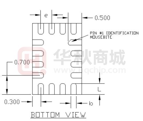
QFN1826-16L
signals in
D1- D1+ D2+ D2-
handset and consumer applications, such as cell
phones, digital cameras, and notebooks with hubs or
12
D0+ 13
controllers with limited USB I/Os.
The WAS4735Q has low bit-to-bit skew and high
channel-to-channel noise isolation, and is compatible
11
10
9
8
D3+
D0- 14
7 D3-
/OE 15
6
NC 16
2
1
with various standards, such as high-speed USB 2.0
3
SEL0
5 SEL1
4
GND D+ D- Vcc
(480Mbps), MHL video 720p/60fps and 1080i/30fps.
Each switch is bi-directional and offers little attenuation
Pin configuration (Top view)
of the high-speed signals at the outputs. Its bandwidth
is quite marginal to pass high-speed differential signals
(2.4Gbps) with good signal integrity.
DF*
The WAS4735Q is featured with special circuitry on
the D+/D-, which allows the device to withstand a
VBUS short to D+ or D- when the USB devices are
either powered off or on.
Marking
DF = Device code
The WAS4735Q is available in QFN1826-16L package.
*
= Month (A~Z)
Standard products are Pb-Free and halogen-Free.
Order information
Device
Package
Shipping
WAS4735Q-16/TR
QFN1826-16L
3000/Reel&Tape
Applications
Cell phones
MID
Router
Features
Other electronics equipments
Supply voltage
: 2.3 ~ 5.5V
-3dB Bandwidth
: 1.2GHz @ CL=0pF
Off isolation
: -50dB @ 250MHz
Crosstalk
: -30dB @ 250MHz
Low quiescent current : 60uA typical
Will Semiconductor Ltd.
1
Jun, 2014 - Rev. 1.1
�WAS4735Q
Pin descriptions
Pin Number
Symbol
Descriptions
1
GND
2
D+
D+ Common Port (HS or FS USB)
3
D-
D- Common Port (HS or FS USB)
4
Vcc
5
SEL1
Path Selection Control Input (See Table Below)
6
SEL0
Path Selection Control Input (See Table Below)
7
D3-
D- From Fourth Source Path (HS or FS USB)
8
D3+
D+ From Fourth Source Path (HS or FS USB)
9
D2-
D- From Third Source Path (HS or FS USB)
10
D2+
D+ From Third Source Path (HS or FS USB)
11
D1+
D+ From Second Source Path (HS or FS USB)
12
D1-
D- From Second Source Path (HS or FS USB)
13
D0+
D+ From First Source Path (HS or FS USB)
14
D0-
D- From First Source Path (HS or FS USB)
15
/OE
Enable Control Input (See Table Below)
16
NC
No Connect
Ground
Power Supply
Function descriptions
SEL0
/OE
SEL1
Function
1
X
X
D+,D- Switch Paths Open
0
0
0
D+ = D0+, D- = D0-
0
0
1
D+ = D1+, D- = D1-
0
1
0
D+ = D2+, D- = D2-
0
1
1
D+ = D3+, D- = D3-
Logic symbol and typical applications
4G
Processor
D0+
D1+
D2+
D3+
D0D1D2D3-
SEL1
SEL0
USB #0
USB Port
D+
2G
modem
USB #1
WAS4735Q
Application
Processor
USB #2
4:1
MUX
D-
Control
Logic Symbol
Will Semiconductor Ltd.
/OE
Vbus
D+
D-
GND
3G
Processor
USB #3
Typical Applications (Mobile Phone Example)
2
Jun, 2014 - Rev. 1.1
�WAS4735Q
Absolute maximum ratings
Parameter
Symbol
Value
Unit
Supply voltage range
VCC
-0.5 ~ 6.5
V
Data input/output voltage range
VDATA
-0.5 ~ 6.5
V
Select input voltage range
VSEL
-0.5 ~ 6.5
V
Continues output current
IOUT
± 50
mA
TJ
150
o
260
o
-65 ~ 150
o
Junction temperature range
Lead temperature range
Storage temperature range
Thermal resistance
TL
TSTG
C
C
C
o
RθJA
250
I/O to VCC, I/O to GND
± 6000
V
I/O to I/O
± 4000
V
Symbol
Value
Unit
Supply voltage range
VCC
2.3 ~ 5.5
V
Data input/output voltage range
VDATA
0.0 ~ VCC
V
Select input voltage range
VSEL
0.0 ~ VCC
V
Enable control input voltage range
VOE
0.0 ~ VCC
ESD protection (HBM)
C/W
Recommend operating ratings
Parameter
Operating temperature range
Will Semiconductor Ltd.
TA
-40 ~ 85
3
V
o
C
Jun, 2014 - Rev. 1.1
�WAS4735Q
o
Electronics Characteristics (Ta=25 C, VCC=4.5V, unless otherwise noted)
Parameter
Symbol
Select and OE logic high level
VIH
Select and OE logic low level
VIL
Supply quiescent current
ICC
Select input leakage current
ISEL
Off state switch leakage current
Conditions
Min.
Typ.
Max.
Unit
VCC=3.0~4.5
1.7
V
VCC=2.3~3.0
1.4
V
VCC=3.0~4.5
0.6
V
VCC=2.3~3.0
0.4
V
80
uA
±1.0
uA
IOFF
±1.0
uA
On state switch leakage current
ION
±1.0
uA
On-Resistance
RON
5.0
7.5
Ω
0.15
0.20
Ω
1.8
2.2
Ω
On-Resistance match
∆ RON
IOUT=0,
VSEL >1.5V or VSEL
很抱歉,暂时无法提供与“WAS4735Q-16/TR”相匹配的价格&库存,您可以联系我们找货
免费人工找货- 国内价格
- 1+1.16199
- 30+1.12049
- 100+1.07899
- 500+0.99600
- 1000+0.95450
- 2000+0.92960


 工商网监
湘ICP备2023018690号
工商网监
湘ICP备2023018690号
