KCT8539S-1
PRELIMINARY DATASHEET
5GHz WLAN 802.11ax Front-End Module
Description
GND
GND
ANT
GND
16
15
14
13
C1
1
12 VDET
C0
2
11
LNA
GND 3
KCT8539S-1 has simple and low-voltage control logic, and requires minimal
external components. A power detector is also integrated for accurately
monitoring of output power from the PA.
10 VCC
KCT8539S-1 is assembled in a compact, low-profile 3x3x0.57mm 16-lead MIS
package. KCT8539S-1 is the ideal RF front-end solution for implementing 5GHz
9 PA_EN high-power WLAN systems supporting multiple standards including
802.11a/n/ac/ax.
PA
VDD 4
5
RX
VCC
KCT8539S-1 is a highly integrated RF Front-End Integrated Circuit incorporates
key RF functionality needed for IEEE 802.11a/n/ac/ax WLAN systems operating
in the 5.15-5.85GHz range. KCT8539S-1 integrates a high-efficiency highlinearity power amplifier (PA), a low noise amplifier (LNA) with bypass, the
associated matching network, LO rejection, and harmonic filters all in one
device.
6
GND
7
GND
8
TX
Applications
802.11ax Wi-Fi Devices
Mini-cards & half mini-cards
Wi-Fi Media Gateways
Consumer Electronics
PC cards, PCMCIA,
Access Points / Routers
Set Top Boxes / Wireless IPTVs
Other 5GHz ISM Platforms
FEATURES
Integrated 802.11ax 5GHz PA, LNA with bypass and T/R switch
Fully-matched input and output
Integrated power detector
Transmit gain: 32dB at 5V
Receive gain: 17dB at 5V
Noise Figure: 1.7dB at 5V
Output power: +21.5dBm @-40dB DEVM, HE160//MCS11, 5V
+22.5dBm @-35dB DEVM, VHT80/MCS9, 5V
+23.5dBm @-30dB DEVM, HT20/MCS7, 5V
ESD protection circuitry on all PINs
Minimal external components required
Small package: MIS16-pin, 3mm x 3mm x0.57mm (MSL3, 260 oC per JEDEC J-STD-020)
ROHS and REACH Compliant
KANGXI Communication Technologies www.kxcomtech.com TEL (+86) 021 6168 1915
This product datasheet is subject to change without notice.
Rev 03
Jan.07,2021
�KCT8539S-1
PRELIMINARY DATASHEET
PIN ASSIGNMENTS
Pin Number
Pin Name
Description
1
C1
Switch Control pin 1
2
C0
Switch Control pin 0
3,6,7,13,15,16,17
GND
Ground – Must be connected to ground in the application circuit
4
VDD
Supply voltage
5
RX
RF output port from LNA or Bypass
8
TX
RF input port from the Transceiver
9
PA_EN
PA enable
10,11
VCC
Supply voltage
12
VDET
Detector output voltage
14
ANT
Antenna port – RF signal from the PA or RF signal applied to the LNA
PIN-OUT DIAGRAM (Top View)
C1
GND
GND
ANT
GND
16
15
14
13
1
12 VDET
17
GND
C0
2
11 VCC
GND
3
10 VCC
VDD
4
9
5
6
7
8
RX
GND
GND
TX
PA_EN
KANGXI Communication Technologies www.kxcomtech.com TEL (+86) 021 6168 1915
This product datasheet is subject to change without notice.
Rev 03
Jan.07,2021
�KCT8539S-1
PRELIMINARY DATASHEET
ABSOLUTE MAXIMUM RATINGS
Parameters
Units
Min
Max
Conditions
DC Supply Voltage
V
-0.5
+6.0
VDD and VCC Pins
DC Input on Control pins
V
-0.5
+3.6
All Control Pins
TX Maximum Input Power (50ohm load, NO Damage)
dBm
+17
LNA On Mode Maximum Input Power
dBm
+18
Bypass Mode Maximum Input Power
dBm
+26
Storage Temperature
oC
Junction Temperature
oC
+165
oC/W
+35
Thermal Resistance(θJC)
-40
+150
NOTE: Sustained operation at or above the Absolute Maximum Ratings for any one or combinations of the above
parameters may result in permanent damage to the device and is not recommended.
All Maximum RF Input Power Ratings assume 50-ohm terminal impedance.
NOMINAL OPERATING CONDITIONS
Parameters
Units
Min
Typical
Max
DC Supply Voltage
V
4.75
5
5.25
Control Pin Voltage- Logic High
V
1.6
3.6
Control Pin Voltage- Logic Low
V
0
0.4
Control Pin DC Current
PAEN
C1
C0
uA
Operating Temperature
oC
400
330
330
-40
+25
Conditions
VDD and VCC Pins
VCC=VDD=3.3V
+85
KCT8539S-1 ELECTRICAL SPECIFICATIONS
(VCC=VDD=5V, T = 25 oC, All Unused Ports Terminated with 50Ω, Unless Otherwise Noted)
Parameters
Frequency Range
Units
Min
GHz
5.15
Typ
Max
Conditions
5.85
Transmit Mode
Small Signal Gain
Output Power
dB
dBm
32
+21.5
HE160/MCS11, -40dB DEVM, Preamble only
+22.5
VHT80/MCS9, -35dB DEVM, Preamble only
+23.5
HT20/MCS7, -30dB DEVM, Preamble only
+26.5
HT20/MCS0, Mask Compliance
KANGXI Communication Technologies www.kxcomtech.com TEL (+86) 021 6168 1915
This product datasheet is subject to change without notice.
Rev 03
Jan.07,2021
�KCT8539S-1
PRELIMINARY DATASHEET
Parameters
Output Power of P1dB
Current
Units
dBm
mA
Min
Typ
Max
Conditions
29.5
160
280
300
325
435
100% duty modulated signal
@No RF
@+21.5dBm
@+22.5dBm
@+23.5dBm
@+26.5dBm
Harmonic
2nd Harmonics
3rd Harmonics
dBm/MHz
-35
-50
Input Return Loss
dB
10
Output Return Loss
dB
8
Isolation
dB
44
13
0.20
0.34
0.75
0.81
0.91
Power Detector Output
V
Power Detector Output
Impedance
ohm
3K
Gain
dB
17
Gain @2.4G band
dB
-21
dBm
-5
Noise Figure
dB
1.7
Input Return Loss
dB
8
Output Return Loss
dB
8
Isolation
dB
22
39
Switching Time
ns
200
200
RX Current
mA
30
dB
4
dBm
22
Input Return Loss
dB
13
Output Return Loss
dB
7
Isolation
dB
44
39
Bypass Current
mA
1
Pout=+26.5dBm,HT20-MCS0 Signal
From ANT to RX Pin
From TX to RX Pin
100% duty modulated signal
@No RF
@+10dBm
@+21.5dBm
@+23.5dBm
@+26.5dBm
Receive Mode – LNA On
Input Power of P1dB
From ANT to TX Pin
From RX to TX Pin
From 50% logic level change to 90%/10% power level
LNA Bypass
RX TX
Receive Bypass Mode
Insertion Loss
Input Power of P1dB
From ANT to TX Pin
From RX to TX Pin
KANGXI Communication Technologies www.kxcomtech.com TEL (+86) 021 6168 1915
This product datasheet is subject to change without notice.
Rev 03
Jan.07,2021
�KCT8539S-1
PRELIMINARY DATASHEET
PRODUCT QUALIFICATION
Parameters
Units
Min
Max
Conditions
ESD – Human Body Mode
V
1500
HBM
ESD – Charge Device Mode
V
2000
CDM
ESD HANDLING:
Although this device is designed to be as robust as possible, electrostatic discharge (ESD) can
damage this device. This device must be protected at all times from ESD when handling or
transporting. Static charges may easily produce potentials of several kilovolts on the human body or
equipment, which can discharge without detection.
Industry-standard ESD handling precautions should be used at all times.
CONTROL LOGIC TABLE
PA_EN
C1
C0
Mode of Operation
1
1
0
Transmit Mode
0
0
1
Receive LNA Mode
0
1
1
Bypass Mode
0
0
0
Shutdown Mode
Note: “1” denotes high voltage state (>1.6V)
“0” denotes low voltage state (
很抱歉,暂时无法提供与“KCT8539S-1”相匹配的价格&库存,您可以联系我们找货
免费人工找货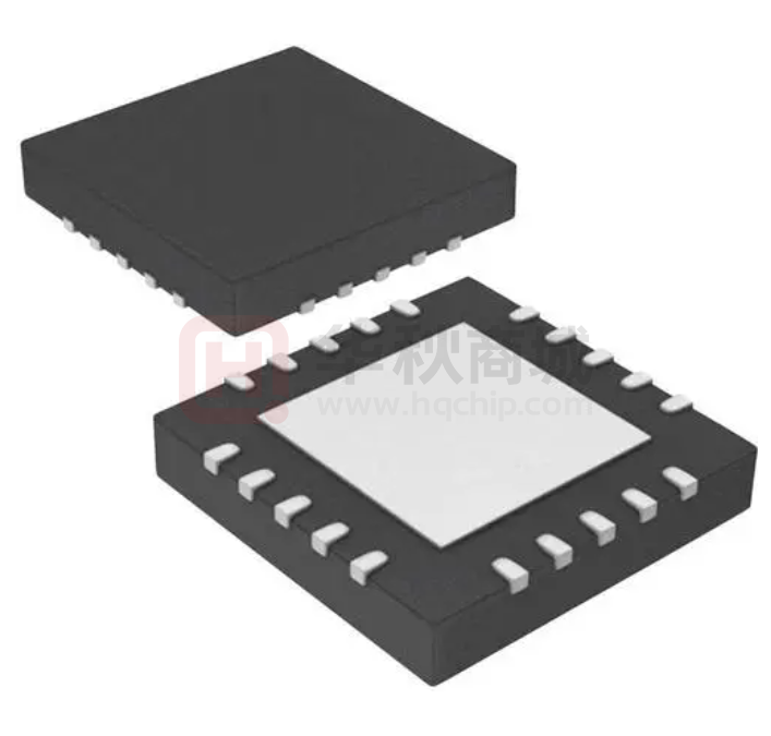


 工商网监
湘ICP备2023018690号
工商网监
湘ICP备2023018690号
