HE2280 series
80V 150mA Low Power LDO
Features
• Low Power Consumption: 2µA (Typ)
• Maximum Output Current: 150mA
• Small Dropout Voltage
•
•
•
•
•
•
700mV@100mA (Vout=3.3V)
• High Input Voltage: Up to 80V
• High Accurate:
Good Transient Response
Integrated Short-Circuit Protection
Over-Temperature Protection
Output Current Limit
Stable with Ceramic Capacitor
Support Fixed Output Voltage
3.3 and 5.0V
HE2280(A) ±1% Output Voltage
• Available Package
• RoHS Compliant and Lead (Pb) Free
SOT23-3 \ SOT89-3
Application
• Portable, Battery Powered Equipment
• Battery-powered equipment
• Weighting Scales
• Smoke detector and sensor
• Car Audio/Video Equipmen
• Home Automation
Description
The HE2280 series is a high voltage,ultralow-power,low dropout voltage
regulator. The device can deliver 150mA output current with a dropout voltage
of 700mV and allows an input voltage as high as 80V. The typical quiescent
current is only 2µA. The device is available in fixed output voltages of 3.3,and
5.0V.The device features integrated short-circuit and thermal shutdown
protection.Although designed primarily as fixed voltage regulators, the device
can be used with external components to obtain variable voltages.
Selection Table
Part No.
Output Voltage
HE2280A33PR
3.3V
SOT89-3
****
HE2280A50PR
5.0V
SOT89-3
****
HE2280A33MR
3.3V
SOT23-3
****
HE2280A50MR
5.0V
SOT23-3
****
Ver1.2
Package
1
Marking
Aug 3,2021
�HE2280 series
80V 150mA Low Power LDO
Application Circuits
VIN
VIN
VOUT
VOUT
GND
10uF
10uF
CIN
COUT
Note:External Component Recommendation:(VIN>45V)
1)
CIN=100uF/100V(Electrolysis)
2)
VIN/R1=50R(0805)
Pin Assignment
Function Block Diagram
Ver1.2
2
Aug 3,2021
�HE2280 series
80V 150mA Low Power LDO
Absolute Maximum Ratings
(1) (2)
Parameter
Symbol
Maximum Rating
Unit
VIN
VSS -0.3~VSS+80.0
V
VOUT
VSS -0.3~VSS+6.0
V
IOUT
400
mA
Input Voltage
Output Current
Power Dissipation
Thermal Resistance
SOT23-3
400
Pd
SOT89-3
SOT23-3
RθJA
SOT89-3
mW
500
(3)
250
℃/W
200
℃/W
Operating Temperature
Topr
-40~85
℃
Storage Temperature
Tstg
-40~125
℃
Soldering Temperature & Time
Tsolder
260℃, 10s
Note (1): Exceeding these ratings may damage the device.
Note (2): The device is not guaranteed to function outside of its operating conditions
Note (3): The package thermal impedance is calculated in accordance to JESD 51-7.
ESD Ratings
Item
Description
Value
Unit
V(ESD-HBM)
Human Body Model (HBM)
ANSI/ESDA/JEDEC JS-001-2014
Classification, Class: 2
±4000
V
V(ESD-CDM)
Charged Device Mode (CDM)
ANSI/ESDA/JEDEC JS-002-2014
Classification, Class: C0b
±200
V
JEDEC STANDARD NO.78E APRIL 2016
Temperature Classification, Class: I
±150
mA
ILATCH-UP
ESD testing is performed according to the respective JESD22 JEDEC standard.The human body model is a 100 pF capacitor discharged
through a 1.5kΩ resistor into each pin. The machine model is a 200pF capacitor discharged directly into each pin.
Recommended Operating Conditions
Parameter
MIN.
MAX.
Units
Supply voltage at VIN
---
60
V
Operating junction temperature range, Tj
-40
125
°C
Operating free air temperature range, TA
-40
85
°C
Note : All limits specified at room temperature (TA = 25°C) unless otherwise specified. All room temperature limits are 100% production
tested. All limits at temperature extremes are ensured through correlation using standard Statistical Quality Control (SQC) methods. All
limits are used to calculate Average Outgoing Quality Level (AOQL).
Ver1.2
3
Aug 3,2021
�HE2280 series
80V 150mA Low Power LDO
Electrical Characteristics
(Test Conditions:VIN= Vset+1V, VOUT=Vset,CIN=10uF, COUT=10uF,TA=25℃, unless otherwise specified.)
Parameter
Symbol
Input Voltage
VIN
Supply Current
IQ
VIN=12V
ILOAD=0mA
—
VOUT1
VIN=12V
IOUT=10mA
VOUT2
Maximum Output
Current
IOUT(Max)
Dropout Voltage
VDROP
VOUT=3.3V
Output Voltage
HE2280 (A)
Output Voltage
HE2280 (B)
(1)
Line Regulation
ΔVOUT/
ΔVIN•VOUT
Load Regulation
ΔVOUT
Short Current
Power Supply
Rejection Rate
Output Noise
Voltage
ISHORT
Output Voltage
Temperature
Coefficient
PSRR
eNO
ΔVOUT/
ΔT•VOUT
Conditions
Max
Units
80
V
2.0
3.0
uA
Vset*0.99
Vset
Vset*1.01
V
VIN=12V
IOUT=10mA
Vset*0.98
Vset
Vset*1.02
V
—
—
200
—
mA
VIN= Vset-0.1V
IOUT=10Ma
—
70
—
VIN= Vset-0.1V
IOUT=100mA
IOUT=1mA
(Vset+0.5v)≦VIN≦55V
VIN=12V
1mA≦IOUT≦100mA
Min
Typ
mV
—
700
—
—
0.01
—
%/V
—
0.02
—
%/ mA
RL=1Ω
VIN=12V VOUT=3.3V
f=1KHz,IOUT= 10mA
COUT=1uF
BW = 300Hz~50kHz
—
80
—
mA
—
70
—
dB
—
50
—
uVRMS
IOUT=10mA
—
100
—
ppm/℃
Note:
(1)Dropout Voltage is the voltage difference between the input and the output at which the output
voltage drops 2% below its nominal value.
Ver1.2
4
Aug 3,2021
�HE2280 series
80V 150mA Low Power LDO
Typical Performance Characteristics:
Test Condition: TA=25°C,IOUT=1mA, COUT=10uF, unless otherwise noted
Ver1.2
5
Aug 3,2021
�HE2280 series
80V 150mA Low Power LDO
H
E
2
0
2
1
A
x
x
Ver1.2
6
Aug 3,2021
�HE2280 series
80V 150mA Low Power LDO
Application Guideline
Input Capacitor
A 10μF ceramic capacitor is recommended to connect between VDD and GND pins to decouple input
power supply glitch and noise. The amount of the capacitance may be increased without limit. This
input capacitor must be located as close as possible to the device to assure input stability and less
noise. For PCB layout, a wide copper trace is required for both VIN and GND.
Output Capacitor
An output capacitor is required for the stability of the LDO. The recommended output capacitance is
10μF, ceramic capacitor is recommended, and temperature characteristics are X7R or X5R. Higher
capacitance values help to improve load/line transient response. The output capacitance may be
increased to keep low undershoot/overshoot. Place output capacitor as close as possible to VOUT
and GND pins.
Dropout Voltage
The dropout voltage refers to the voltage difference between the VIN and VOUT pins while operating
at specific output current. The dropout voltage VDROP also can be expressed as the voltage drop on
the pass-FET at specific output current (IRATED) while the pass-FET is fully operating at ohmic
region and the pass-FET can be characterized asan resistance RDS(ON). Thus the dropout voltage
can bedefined as (VDROP = VIN − VOUT = RDS(ON) x IRATED). Fornormal operation, the
suggested LDO operating range is (VIN > VOUT + VDROP) for good transient response and PSRR
ability. Vice versa, while operating at the ohmic region will degrade the performance severely.
Thermal Application
For continuous operation, do not exceed the absolute maximum junction temperature. The maximum
power dissipation depends on the thermal resistance of the IC package, PCB layout, rate of
surrounding airflow, and difference between junction and ambient temperature. The maximum power
dissipation can be calculated as below: TA=25°C, PCB,
The max PD= (125°C − 25°C) / (Thermal Resistance °C/W)
Power dissipation (PD) is equal to the product of the output current and the voltage drop across the
output pass element, as shown in the equation below:
PD = (VIN – VOUT) × IOUT
Ver1.2
7
Aug 3,2021
�HE2280 series
80V 150mA Low Power LDO
Packaging Information
SOT23-3L
Ver1.2
8
Aug 3,2021
�HE2280 series
80V 150mA Low Power LDO
3-pin SOT89 Outline Dimensions
Ver1.2
9
Aug 3,2021
�
很抱歉,暂时无法提供与“HE2280A33MR”相匹配的价格&库存,您可以联系我们找货
免费人工找货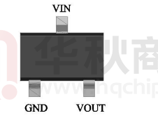


 工商网监
湘ICP备2023018690号
工商网监
湘ICP备2023018690号
