CMSA80P06
P-Channel Enhancement Mode Field Effect Transistor
General Description
Product Summary
The CMSA08P06 uses advanced
BVDSS
RDSON
ID
-60V
15mΩ
-80A
technology to provide excellent
RDS (ON) . This device is suitable
Applications
to be used as the low side FET
Load Switch
in SMPS,load switching and
Power Management in Notebook Computer,Portable
general purpose.
Equipment and Battery Powered Systems.
Features
DFN-8 5x6 Pin Configuration
Fast switching speed
D
D
D
D
D
Lower On-resistance
100% EAS Guaranteed
S
Simple Drive Requirement
Pin 1
Absolute Maximum Ratings
Symbol
Parameter
S
S
G
G
S
DFN-8 5x6
Type
Package
Marking
CMSA80P06
DFN-8 5*6
CMSA80P06
Rating
Units
VDS
Drain-Source Voltage
-60
V
VGS
Gate-Source Voltage
±20
V
ID@TC=25℃
Continuous Drain Current
-80
A
IDM
Pulsed Drain Current
-240
A
1
EAS
Single Pulse Avalanche Energy
480
mJ
PD@TC=25℃
Total Power Dissipation
95
W
TSTG
Storage Temperature Range
-55 to 150
℃
TJ
Operating Junction Temperature Range
-55 to 150
℃
Thermal Data
Symbol
Parameter
RθJA
Junction-to-Ambient
RθJC
Junction-to-Case
CA03R1
www.cmosfet.com
Typ.
Max.
Unit
---
62
℃/W
---
1.3
℃/W
Page 1 of 2
�CMSA80P06
P-Channel Enhancement Mode Field Effect Transistor
Electrical Characteristics (TJ=25℃ , unless otherwise noted)
Symbol
Parameter
BVDSS
Drain-Source Breakdown Voltage
RDS(ON)
Static Drain-Source On-Resistance
VGS(th)
Min.
Typ.
Max.
Unit
VGS=0V , ID=-250uA
Conditions
-60
---
---
V
VGS=-10V, ID=-28A
---
---
15
VGS=-4.5V, ID=-20A
---
---
19
Gate Threshold Voltage
VGS=VDS , ID =-250uA
-1
---
-3
V
IDSS
Drain-Source Leakage Current
VDS=-48V , VGS=0V , TJ=25℃
---
---
-1
uA
IGSS
Gate-Source Leakage Current
VGS = ±20V , VDS=0V
---
---
±100
nA
mΩ
gfs
Forward Transconductance
VDS=-10V , ID=-28A
---
40
---
S
Rg
Gate Resistance
VDS=0V , VGS=0V , f=1MHz
---
3.5
---
Ω
Qg
Total Gate Charge
---
88
---
Qgs
Gate-Source Charge
---
11
---
Qgd
Td(on)
Tr
Td(off)
Tf
Gate-Drain Charge
VDS=-30V , ID=-17A
VGS=-10V
Turn-On Delay Time
---
31
---
---
14
---
Rise Time
VDD=-30V, RG=6Ω
---
12
---
Turn-Off Delay Time
ID=-1A , RL =30Ω , VGEN =-10V
---
110
---
nC
ns
Fall Time
---
61
---
Ciss
Input Capacitance
---
7600
---
Coss
Output Capacitance
---
501
---
Crss
Reverse Transfer Capacitance
---
291
---
Min.
Typ.
Max.
Unit
---
---
-80
A
---
---
-240
A
---
---
-1.2
V
VDS=-30V, VGS=0V , f=1MHz
pF
Diode Characteristics
Symbol
Parameter
IS
Continuous Source Current
ISM
Pulsed Source Current
VSD
Diode Forward Voltage
Conditions
VG=VD=0V , Force Current
VGS=0V , IF =-28A
Note :
1.The test condition is VDD=30V , VGS=10V , L=0.5mH , IAS=44A
This product has been designed and qualified for the counsumer market.
Cmos assumes no liability for customers' product design or applications.
Cmos reserver the right to improve product design ,functions and reliability wihtout notice.
CA03R1
www.cmosfet.com
Page 2 of 2
�
很抱歉,暂时无法提供与“CMSA80P06”相匹配的价格&库存,您可以联系我们找货
免费人工找货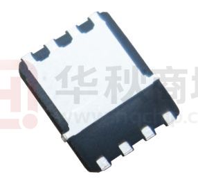


 工商网监
湘ICP备2023018690号
工商网监
湘ICP备2023018690号
