XBLW MC33063
1 .5A Step-Up/Down/Inverting Switching Regulator
General
Description
The MC33063 is a monolithic control circuit containing the primary
functions required for DC- to- DC converters. This device consists of an
internal temperature compensated reference ( 1.25V ) ,comparator,
controlled duty cycle oscillator with an active current limit circuit, driver
and high current output switch. The IC is specifically designed to be used
in Step- Down and Step- Up and Voltage- Inverting applications with a
minimum number of external components.
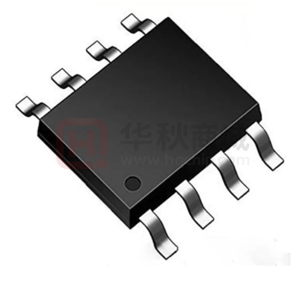
The MC33063 is available in DIP8 and SOP8 package.
F eatu res
FunctionalBlockDiagram
Operation from 3.0V to 40V Input
Low Standby Current
Current Limiting
Output Switch Current to 1.5A
Output Voltage Adjustable
Frequency Operation to 100kHz
Precision 2% Reference
Ordering
Information
DEVICE
XBLW MC33063ADTR
XBLWversion1 . 0
Package Type
MARKING
SOP-8
MC33063A
Packing
Tape
文档仅供参考,实际应用测试为准
www.xinboleic.com
技术支持热线:4009682003
Packing QTY
2500/Reel
第 1页 共 9页
�XBLW MC33063
1.5 A Step-Up/Down/Inverting Switching Regulator
Pin
Configuration
Pin
Description
Pin Number
Pin Name
Function Description
Pin Number
Pin Name
Function Description
1
SC
Switch collector
5
FB
Comparator inverting input
2
SE
Switch emitter
6
V CC
Input voltage
3
CT
Timing capacitor
7
Ipk
Ipk sense
4
GND
Ground
8
DC
Drive collector
Absolute Maximum Ratings ( Ta= 2 5 ° C)
Symbol
Value
Unit
Power Supply Voltage
Vcc
40
V
Comparator Input Voltage Range
V IR
-0.3~40
V
Switch Collector Voltage
Vc( switch)
40
V
Switch Emitter Voltage (VPin1=40 V)
VE (switch)
40
V
Switch Collector to Emitter Voltage
VCE( switch)
40
V
Driver Collector Voltage
Vc( drive)
40
V
Driver Collector Current
Ic(drive)
100
mA
ISW
1.5
A
Parameter Name
Switch Current
DIP8
Power Dissipation
1.25
W
625
mW
Ta
0~70
Tstg
-65~ 150
℃
PD
SOP8
Operating Ambient Temperature Range
Storage Temperature Range
℃
Electrical Characteristics ( Unless otherwise noted , Vcc= 5 . 0 V, Ta= 0 ~ 7 0 ° C)
Symbol
Min
Typ
Max
Unit
Frequency (Vpin5=0V,CT=1.0nF, Ta=25°C)
fosc
24
33
42
kHz
Charge Current (Vcc=5.0~40V, Ta=25°C)
Ichg
24
35
42
pA
Idischg
140
220
260
pA
Idischg/ Ichg
5.2
6.5
7.5
Vipk( sense)
250
300
350
Parameter Name
OSCILLATOR
Discharge Current (Vcc=5.0~40V, Ta=25°C)
Discharge to Charge Current Ratio
(Pin7 to Vcc, Ta=25°C)
Current limit Sense Voltage
(Ichg=Idischg, Ta=25°C)
XBLWversion1 . 0
文档仅供参考,实际应用测试为准
www.xinboleic.com
技术支持热线:4009682003
mA
第 2页 共 9页
�XBLW MC33063
1.5 A Step-Up/Down/Inverting Switching Regulator
OUTPUT SWITCH
Saturation Voltage, Darlington Connection
(ISW=1.0A, Pins 1,8 Connected)
Saturation Voltage, Darlington Connection
(ISW=1.0A, Rpin 8=82Ω to Vcc, Forced β ≈ 20)
DC Current Gain (ISW=1.0A,VCE=5.0V, Ta=25°C)
Collector Off- State Current (VCE=40 V)
VCE( sat)
1.0
1.3
V
VCE( sat)
0.45
0.7
V
0.01
100
pA
1.25
1.275
hFE
50
Ic(off)
75
COMPARATOR
Threshold Voltage (Ta=25 °C)
Vth
Threshold Voltage (Ta=0~70 °C)
Threshold Voltage Line Regulation
(Vcc=3.0~40V)
Input Bias Current(Vin=0 V)
1.225
1.21
1.29
V
Regline
1.4
5.0
mV
IIB
-20
-400
nA
4.0
mA
TOTAL DEVICE
Supply Current (Vcc=5.0~40V, CT=1.0nF,
Pin7= Vcc, Vpin5> Vth, pin2= Gnd, Remaining Pins Open)
Icc
Characteristics Curves
XBLWversion1 . 0
文档仅供参考,实际应用测试为准
www.xinboleic.com
技术支持热线:4009682003
第 3页 共 9页
�XBLW MC33063
1.5 A Step-Up/Down/Inverting Switching Regulator
Typical
1.
Application
Step- Up Converter
Test
Conditions
Results
Line Regulation
Vin=8.0V~ 16V, Io= 175mA
30mV=±0.05%
Load Regulation
Vin= 12V,Io=75mA~ 175mA
10mV=±0.017%
Output Ripple
Vin= 12V, Io= 175mA
400mVpp
Efficiency
Vin=12V, Io= 175mA
87.7%
Output Ripple With Optional Filter
Vin=12V, Io= 175mA
40mVpp
XBLWversion1 . 0
文档仅供参考,实际应用测试为准
www.xinboleic.com
技术支持热线:4009682003
第 4页 共 9页
�XBLW MC33063
1.5 A Step-Up/Down/Inverting Switching Regulator
2.
Step-Down Converter
Test
Conditions
Results
Line Regulation
Vin=15V~25V, Io=500mA
12mV=±0. 12%
Load Regulation
Vin=25V,Io=50mA~500mA
3.0mV=±0.03%
Output Ripple
Vin=25V, Io=500mA
120mVpp
Short Circuit Current
Vin=25V,RL=0. 1Ω
1. 1A
Efficiency
Vin=25V, Io=500mA
83.7%
Output Ripple With Optional Filter
Vin=25V, Io=500mA
40mVpp
3 . Voltage Inverting Converter
XBLWversion1 . 0
文档仅供参考,实际应用测试为准
www.xinboleic.com
技术支持热线:4009682003
第 5页 共 9页
�XBLW MC33063
1 .5A Step-Up/Down/Inverting Switching Regulator
Test
Conditions
Results
Line Regulation
Vin=4.5V~6.0V, Io= 100mA
3.0mV=±0.012 %
Load Regulation
Vin=5.0V,Io= 10mA~ 100mA
0.022V=±0.09%
Output Ripple
Vin=5.0V, Io= 100mA
500mVpp
Short Circuit Current
Vin=5.0V,RL=0. 1Ω
910mA
Efficiency
Vin=5.0V, Io= 100mA
62.2%
Output Ripple With Optional Filter
Vin=5.0V, Io= 100mA
70mVpp
Application Information
XBLWversion1 . 0
文档仅供参考,实际应用测试为准
www.xinboleic.com
技术支持热线:4009682003
第 6页 共 9页
�XBLW MC33063
1 .5A Step-Up/Down/Inverting Switching Regulator
Vsat = Saturation voltage of the output switch
VF = Forward voltage drop of the output rectifier
The following power supply characteristics must be chosen:
Vin — Nominal input voltage
Vout — Desired output voltage , | Vout |= 1.25 × ( 1 +R2 /R1)
Iout — Desired output current
fmin — Minimun desired output switching frequency at the selected values of Vin and Io
Vripple( pp) — Desired peak−to −peak output ripple voltage. In practice, the calculated capacitor value will need to be
increased due to its equivalent series resistance and board layout. The ripple voltage should be kept to a low value since
it will directly affect the line and load regulation.
Outline
Dimensions
Unit: mm
DIP8
33063
Un it: mm
SOP8
XBLWversion1 . 0
文档仅供参考,实际应用测试为准
www.xinboleic.com
技术支持热线:4009682003
第 7页 共 9页
�XBLW MC33063
1 .5A Step-Up/Down/Inverting Switching Regulator
33063
XBLWversion1 . 0
文档仅供参考,实际应用测试为准
www.xinboleic.com
技术支持热线:4009682003
第 8页 共 9页
�XBLW MC33063
1 .5A Step-Up/Down/Inverting Switching Regulator
Statement:
Shenzhen xinbole electronics co., ltd. reserves the right to change the product specifications, without notice!
Before placing an order, the customer needs to confirm whether the information obtained is the latest version,
and verify the integrity of the relevant information.
Any semiconductor product is liable to fail or malfunction under certain conditions, and the buyer shall be
responsible for complying with safety standards in the system design and whole machine manufacturing using
Shenzhen xinbole electronics co. , ltd products, and take appropriate security measures to avoid the potential risk
of failure may result in personal injury or property losses of the situation occurred!
Product performance is never ending, Shenzhen xinbole electronics co., ltd will be dedicated to provide
customers with better performance, better quality of integrated circuit products.
XBLWversion1 . 0
文档仅供参考,实际应用测试为准
www.xinboleic.com
技术支持热线:4009682003
第 9页 共 9页
�


 工商网监
湘ICP备2023018690号
工商网监
湘ICP备2023018690号
