650V, 20mΩ, TO-247-4L SiC MOSFET
H1M065Q020 Device Datasheet
Product Summary
H1M065Q020
VDS
ID(@25°C)
RDS(on)
Silicon Carbide MOSFET
N-CHANNEL ENHANCEMENT MODE
Features
◼
◼
◼
◼
◼
◼
Low On-Resistance and High Current Density
Low Capacitance for High Frequency Operation
Ultra-high Avalanche Ruggedness
Positive Temperature Coefficient Device
Low impedance Kelvin source pin-out
RoHS Compliant and Halogen Free
Circuit Diagram
D (1)
G (4)
(4)
(3)
(2)
(1)
Benefits
◼
◼
◼
◼
◼
Higher System Efficiency
Increase Parallel Device Convenience
Capable of 175°C High Tj Application
Allow High Frequency Operation
Realize Compact and Lightweight Systems
SS (3)
S (2)
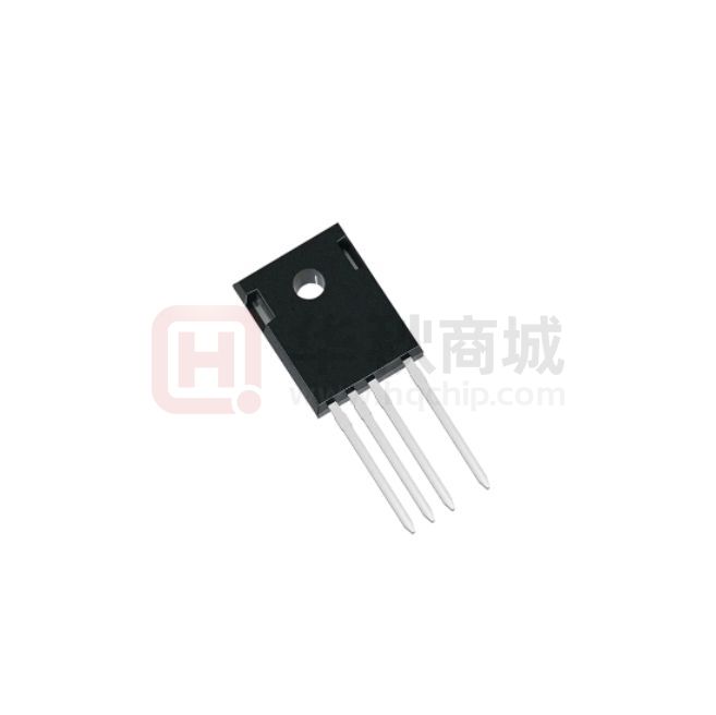
Part Number
Package
Marking
H1M065Q020
TO-247-4L
H1M065Q020
Description
The H1M065Q020 650V, 20mΩ silicon carbide power
MOSFET is an N-channel enhancement mode device.
Exploiting the outstanding wide bandgap material
properties, this device shows high current density and
great switching behavior. Thanks for the excellent
thermal conductivity and many advantages of SiC, this
device significantly improved in thermal capability and
temperature independent switching behavior.
Applications
◼
◼
◼
◼
◼
◼
650V
115A
20mΩ
Switching Mode Power Supply
DC/DC Converters, UPS, and PFC
EV Charging Station
Motor Drives
Power Inverters
Solar/Wind Renewable Energy
Absolute Maximum Ratings (T = 25°C unless otherwise specified)
c
Parameter
Symbol
Test Conditions
Value
Unit
Drain – Source Voltage
VDS, max
ID
Pulse Drain Current
Avalanche energy, Single Pulse
Power Dissipation
ID, pulse
EAS
PD
650
115
72
281
3.2
375
V
Continuous Drain Current
Recommend Gate Source Voltage
VGS, op
Maximum Gate Source Voltage
VGS, max
VGS=0V, IDS=100A
VGS=20V, TC=25°C
VGS=20V, TC=110°C
tPW limitation per Fig.15
VDD=100V, ID=14A
TC=25°C
Static, recommended DC operating
values
Transient operating limit
(AC f > 1Hz, duty cycle < 1%)
Junction & Storage Temperature
Soldering Temperature
Mounting Torque
Tj , Tstg
TL
MD
A
J
W
-5 to 20
V
-10 to 25
-55 to 175
260
1.0
M3 or 6-32 screw
°C
Nm
Thermal Resistance
Parameter
Symbol
Thermal Resistance, Junction to Case
Rθ,JC
H1M065Q020 Rev. Preliminary 0.6
Oct. 2023
1
Min.
Typ.
0.4
Max.
Unit
°C/W
www.hestiapower.cn
© Hestia Power
�650V, 20mΩ, TO-247-4L SiC MOSFET
H1M065Q020 Device Datasheet
Electrical Characteristics (T = 25°C unless otherwise specified)
c
Parameter
Symbol
Test Conditions
Drain-Source Breakdown Voltage
Gate Threshold Voltage
V(BR)DSS
VGS(th)
Zero Gate Voltage Drain Current
IDSS
Gate-Source Leakage Current
IGSS
VGS=0V, IDS=100A
VDS=10V, IDS=50mA
VDS=650V, VGS=0V
VDS=650V, VGS=0V
Tj=175°C
VGS=20V, VDS=0V
VGS=20V, IDS=50A
VGS=20V, IDS=50A,
Tj=175°C
VDS=10V, IDS=60A
Drain-Source On-State Resistance
RDS(on)
Transconductance
Input Capacitance
Output Capacitance
Reverse Transfer Capacitance
Effective Output Capacitance, Energy
Related
Effective Output Capacitance, Time
Related
gfs
Ciss
Coss
Crss
Short-Circuit Withstand Time
tSC
Turn On Delay Time
Rise Time
Turn Off Delay Time
Fall Time
td(on)
tr
td(off)
tf
Coss Stored Energy
Eoss
Turn-on Switching Energy
Eon
Turn-off Switching Energy
Internal Gate Resistance
Eoff
RG(int.)
VGS=0V, VDS=400V
f =1MHz, VAC=25mV
Co(er)
Co(tr)
VGS=0V,
VDS=0 to 400V
ID=const., VGS=0V,
VDS=0 to 400V
VGS=0/15V, VDS=400V
RG=100Ω
VDS=400V, VGS=-4/+20V,
ID=35A, RL=11.4Ω,
RG(ext)= 2.7 Ω
VGS=0V, VDS=400V
f =1MHz, VAC=25mV
VDS=400V, VGS=0/20V,
ID=50A,
RG(ext)= 2.7 Ω
f =1MHz, VAC=25mV
Min.
650
Typ.
Max.
2.2


 工商网监
湘ICP备2023018690号
工商网监
湘ICP备2023018690号
