RF-BM-2652P4(I)
www.szrfstar.com
V1.0 - May, 2023
RF-BM-2652P4 and RF-BM-2652P4I CC2652P7
SimpleLink™ Multiprotocol 2.4 GHz Wireless Module
with Integrated Power Amplifier
Version 1.0
Shenzhen RF-star Technology Co., Ltd.
May 25th, 2023
All rights reserved. Those responsible for unauthorized reproduction will be prosecuted.
Shenzhen RF-star Technology Co., Ltd.
Page 1 of 23
�RF-BM-2652P4(I)
www.szrfstar.com
V1.0 - May, 2023
1 Device Overview
1.1 Description
RF-BM-2652P4(I) is an RF module based on TI lower-power CC2652P7 SoC, which is a multiprotocol 2.4 GHz wireless
module supporting Matter, Thread, Zigbee®, Bluetooth® 5.3 Low Energy, IEEE 802.15.4, IPv6-enabled smart objects
(6LoWPAN), proprietary systems, including the TI 15.4-Stack (2.4 GHz), and concurrent multiprotocol through a
Dynamic Multiprotocol Manager (DMM) driver. It integrates a 48 MHz crystal and a 32.768 kHz crystal, 704 KB of
in-system Programmable Flash, 256 KB ROM, 8 KB of Cache SRAM, and 144 KB of ultra-low leakage SRAM. Its ARM®
Cortex®-M4F core application processor can operate at an extremely low current at flexible power modes. And the
module enables long-range and low-power applications using an integrated +20 dBm high-power amplifier with
best-in-class transmit current consumption at 101 mA. It features a small size, robust connection distance, and rigid
reliability. Optional antenna output modes (PCB, IPEX connector, and half-hole interface) make the module more
convenient for application and development.
1.2 Key Features
• RF Features
• Memory
- Bluetooth® 5.3 Low Energy
- Matter,
ZigBee®,
- 704 KB of in-system programmable flash
Thread
- 256 KB of ROM for protocols and library
- Proprietary systems
functions
- IEEE 802.15.4
- 8 KB of cache SRAM (Alternatively available as
- IPv6-enabled smart objects (6LoWPAN)
-
SimpleLinkTM
TI 15.4-Stack (2.4 GHz)
general-purpose RAM)
- 144 KB of ultra-low leakage SRAM. The SRAM
- Dynamic Multiprotocol Manager (DDM) driver
• TX power: up to +20 dBm with temperature
is protected by parity to ensure high reliability of
operation.
• Ultra-low power sensor controller with 4 KB of
compensation
• Excellent receiver sensitivity
SRAM
- -99 dBm for 802.15.4 (2.4 GHz)
- Sample, store, and process sensor data
- -104 dBm for Bluetooth 125 kbps (LE coded PHY)
- Operation independent from system CPU
• Wide Operation Range
- Fast wake-up for low-power operation
• Rich Peripherals
- 1.8 V to 3.8 V single power supply
- Operating temperature: -40 °C to +85 °C
- Storage temperature: -40 °C to +125 °C
• Microcontroller
- Powerful 48 MHz
- Digital peripheral pins can be routed to 23
GPIOs
- 4 × 32-bit or 8 × 16-bit general-purpose timers
ARM®
Cortex®-M4F
processor
- 12-bit ADC, 200 ksamples/s, 8 channels
- EEBMC CoreMark® score: 148
- 2 × comparators
- 2-pin cJTAG and JTAG debugging
- Programmable current source
- Support OTA upgrade
- 2 × UART
Shenzhen RF-star Technology Co., Ltd.
Page 2 of 23
�RF-BM-2652P4(I)
www.szrfstar.com
V1.0 - May, 2023
- 2 × SSI (SPI, Microwave, TI)
- ECC and RSA public key hardware accelerator
- I2C
- SHA2 accelerator (full suite up to SHA-512)
-
I2S
- Real-time clock (RTC)
- Integrated temperature and battery monitor
• Security Enablers
- True random number generator (TRNG)
• External system
- On-chip buck DC/DC converter
• Dimension: 30.0 mm × 16.4 mm × 2.2 mm
- AES 128-bit and 256- bit Crypto accelerator
1.3 Applications
• 2400 to 2480 MH ISM and SRD systems with
down to 4 kHz of receive bandwidth
• Wireless healthcare applications
• Energy harvesting applications
• Home and building automation
• Asset tracking and management
• Building security system
• Electronic Shelf Label (ESL)
• HVAC system
• Wired networking
• Gateway
• Small business router
• IP network camera
• Portable electronics
• Fire safety system
• Set-top box
• Smart grid
• Connected peripherals
• Automatic meter reading
• Keyboard and keypads
• Industrial transport
• Home theater & entertainment
• Wireless sensor networks
• Electronic and robotic toys
• Wearables
• Factory automation and control
Shenzhen RF-star Technology Co., Ltd.
Page 3 of 23
�RF-BM-2652P4(I)
www.szrfstar.com
V1.0 - May, 2023
1.4 Functional Block Diagram
48.0 MHz 32.768 kHz
2.4 GHz
Balun
GPIOs
Jtag
CC2652P7
2.4 GHz
PA Balun
EMI Filter
Control (GPIO)
Half Hole Interface
A
000
PCB Antenna
B
Antenna
Matching
Switch
IPEX Connector
Power Supply Reset
1.8 V ~ 3.8 V
Figure 1. Functional Block Diagram of RF-BM-2652P4(I)
1.5 Part Number Conventions
The part numbers are of the form of RF-BM-2652P4(I) where the fields are defined as follows:
RF - BM - 2652P 4
I
Antenna Type
Company Name
IPEX Connector
Module Version Number
RF-STAR
The Fourth PA Version
Wireless Type
Bluetooth Module
Chipset
CC2652P7
Figure 2. Part Number Conventions of RF-BM-2652P4(I)
Shenzhen RF-star Technology Co., Ltd.
Page 4 of 23
�RF-BM-2652P4(I)
www.szrfstar.com
V1.0 - May, 2023
Table of Contents
1 Device Overview ............................................................................................................................................................. 2
1.1 Description............................................................................................................................................................ 2
1.2 Key Features ....................................................................................................................................................... 2
1.3 Applications .......................................................................................................................................................... 3
1.4 Functional Block Diagram .............................................................................................................................. 4
1.5 Part Number Conventions .............................................................................................................................. 4
Table of Contents................................................................................................................................................................ 5
2 Module Configuration and Functions ...................................................................................................................... 7
2.1 Module Parameters ........................................................................................................................................... 7
2.2 Module Pin Diagram ......................................................................................................................................... 8
2.3 Pin Functions ....................................................................................................................................................... 8
3 Specifications ................................................................................................................................................................. 10
3.1 Recommended Operating Conditions ..................................................................................................... 10
3.2 Handling Ratings.............................................................................................................................................. 10
3.3 PA Output Control ............................................................................................................................................ 10
4 Application, Implementation, and Layout............................................................................................................. 11
4.1 Module Photos .................................................................................................................................................. 11
4.2 Recommended PCB Footprint.................................................................................................................... 11
4.3 Schematic Diagram......................................................................................................................................... 12
4.4 Reference Design ............................................................................................................................................ 13
4.5 Antenna................................................................................................................................................................ 13
4.5.1 Antenna Design Recommendation .............................................................................................. 13
4.5.2 Antenna Output Mode Modification .............................................................................................. 14
4.5.3 External Antenna Design Recommendation of the Half-Hole ANT Pin .......................... 15
4.5.4 IPEX Connector Specification ........................................................................................................ 16
4.6 Basic Operation of Hardware Design ...................................................................................................... 16
4.7 Trouble Shooting .............................................................................................................................................. 17
4.7.1 Unsatisfactory Transmission Distance........................................................................................ 17
4.7.2 Vulnerable Module .............................................................................................................................. 18
4.7.3 High Bit Error Rate ............................................................................................................................. 18
4.8 Electrostatics Discharge Warnings ........................................................................................................... 18
Shenzhen RF-star Technology Co., Ltd.
Page 5 of 23
�RF-BM-2652P4(I)
www.szrfstar.com
V1.0 - May, 2023
4.9 Soldering and Reflow Condition................................................................................................................. 18
5 Optional Package Specification .............................................................................................................................. 20
6 Revision History ............................................................................................................................................................ 22
7 Contact Us....................................................................................................................................................................... 23
Shenzhen RF-star Technology Co., Ltd.
Page 6 of 23
�RF-BM-2652P4(I)
www.szrfstar.com
V1.0 - May, 2023
2 Module Configuration and Functions
2.1 Module Parameters
Table 1. Parameters of RF-BM-2652P4(I)
Chipset
CC2652P7
Supply Power Voltage
1.8 V ~ 3.8 V, 3.3 V is recommended
Frequency
2402 MHz ~ 2480 MHz
Maximum Transmit Power
+20.0 dBm
Receiving Sensitivity
-99 dBm @ 802.15.4 (2.4 GHz)
-104 dBm @ Bluetooth 125 kbps (LE Coded PHY)
GPIO
23
Flash
704 KB
ROM
256 KB
SRAM
152 KB
RX current: 6.4 mA
TX current: 7.3 mA @ 0 dBm
9.7 mA @ 5 dBm
21 mA @ 10 dBm
101 mA @ 20 dBm
Power Consumption
MCU 48 MHz (CoreMark): 3.1 mA (65 μA/MHz)
Sensor Controller: 29.2 μA @ Low Power-Mode, 2 MHz
799 μA @ Active-Mode, 24 MHz
Standby: 0.9 µA
Shutdown: 0.1 µA
Support Protocol
Bluetooth 5.3 Low Energy, Matter, ZigBee, Thread, IEEE 802.15.4, 6LoWPAN,
SimpleLinkTM TI 15.4-stack, Proprietary systems
Crystal
48 MHz, 32.768 kHz
Package
SMT packaging (1.27-mm half-hole pitch stamp stick)
Dimension
30.0 mm × 16.4 mm × 2.2 mm
Type of Antenna
RF-BM-2652P4: PCB antenna
RF-BM-2652P4I: IPEX connector, ANT pin
Operating Temperature
-40 ℃ ~ +85 ℃
Storage Temperature
-40 ℃ ~ +125 ℃
Shenzhen RF-star Technology Co., Ltd.
Page 7 of 23
�RF-BM-2652P4(I)
www.szrfstar.com
V1.0 - May, 2023
2.2 Module Pin Diagram
Figure 3. Pin Diagram of RF-BM-2652P4(I)
2.3 Pin Functions
Table 2. Pin Diagram of RF-BM-2652P4(I)
Pin
Name
Chip Pin
Function
1
DIO5
DIO_5
Digital
GPIO, high-drive capability
2
DIO6
DIO_6
Digital
GPIO, high-drive capability
3
DIO7
DIO_7
Digital
GPIO, high-drive capability
4
DIO8
DIO_8
Digital
GPIO
5
DIO9
DIO_9
Digital
GPIO
6
DIO10
DIO_10
Digital
GPIO
7
DIO11
DIO_11
Digital
GPIO
8
DIO12
DIO_12
Digital
GPIO
9
DIO13
DIO_13
Digital
GPIO
10
RES
RESET_N
Digital
Reset, active low. Internal pullup.
11
JTAG_TMSC
JTAG_TMSC
Digital
JTAG TMSC, high-drive capability
12
JTAG_TCKC
JTAG_TCKC
Digital
JTAG TCKC
Shenzhen RF-star Technology Co., Ltd.
Description
Page 8 of 23
�RF-BM-2652P4(I)
www.szrfstar.com
V1.0 - May, 2023
13
VCC
VCC
-
14
GND
GND
Ground
Ground
15
DIO14
DIO_14
Digital
GPIO
16
DIO15
DIO_15
Digital
GPIO
17
DIO16
DIO_16
Digital
GPIO, JTAG_TDO, high-drive capability
18
DIO17
DIO_17
Digital
GPIO, JTAG_TDI, high-drive capability
19
DIO18
DIO_18
Digital
GPIO
20
DIO19
DIO_19
Digital
GPIO
21
DIO20
DIO_20
Digital
GPIO
22
DIO21
DIO_21
Digital
GPIO
23
DIO22
DIO_22
Digital
GPIO
24
DIO23
DIO_23
Digital or Analog
GPIO, analog capability
25
DIO24
DIO_24
Digital or Analog
GPIO, analog capability
26
DIO25
DIO_25
Digital or Analog
GPIO, analog capability
27
DIO26
DIO_26
Digital or Analog
GPIO, analog capability
28
DIO27
DIO_27
Digital or Analog
GPIO, analog capability
29
GND
GND
Ground
30
ANT
Shenzhen RF-star Technology Co., Ltd.
-
Power supply: 1.8 V ~ 3.8 V, recommended to 3.3 V
Ground
External antenna interface
Page 9 of 23
�RF-BM-2652P4(I)
www.szrfstar.com
V1.0 - May, 2023
3 Specifications
3.1 Recommended Operating Conditions
Functional operation does not guarantee performance beyond the limits of the conditional parameter values in the table
below. Long-term work beyond this limit will affect the reliability of the module more or less.
Table 3. Recommended Operating Conditions of RF-BM-2652P4(I)
Condition
Items
Min.
Typ.
Max.
Unit
Operating Supply Voltage
/
1.8
3.3
3.8
V
Operating Temperature
/
-40
+25
+85
℃
Min.
Typ.
Max.
Unit
-40
+25
+125
℃
3.2 Handling Ratings
Table 4. Handling Ratings of RF-BM-2652P4(I)
Condition
Items
Storage Temperature
Tstg
Human Body Model
HBM
±2000
Moisture Sensitivity Level
V
3
Charged Device Model
±500
V
3.3 PA Output Control
The PA of the CC2652P switches the RF switch by controlling the output of DIO28 and DIO29, and then switches the PA
and non-PA RF output to realize the control of the transmission power range.
Table 3. RF Control Truth Table
Power
DIO28 (Output)
DIO29 (Output)
+5 dBm ~ + 20 dBm (PA)
0
1
< 5 dBm
1
0
Shenzhen RF-star Technology Co., Ltd.
Page 10 of 23
�RF-BM-2652P4(I)
www.szrfstar.com
V1.0 - May, 2023
4 Application, Implementation, and Layout
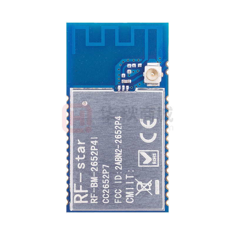
4.1 Module Photos
RF-BM-2652P4
RF-BM-2652P4I
Figure 3. Photos of RF-BM-2652P4(I)
4.2 Recommended PCB Footprint
Figure 4. Recommended PCB Footprint of RF-BM-2652P4(I)
Shenzhen RF-star Technology Co., Ltd.
Page 11 of 23
�RF-BM-2652P4(I)
www.szrfstar.com
V1.0 - May, 2023
4.3 Schematic Diagram
Figure 5. Schematic Diagram of RF-BM-2652P4(I)
Shenzhen RF-star Technology Co., Ltd.
Page 12 of 23
�RF-BM-2652P4(I)
www.szrfstar.com
V1.0 - May, 2023
4.4 Reference Design
Figure 5. Reference Design of RF-BM-2652P4(I)
4.5 Antenna
4.5.1 Antenna Design Recommendation
1. The antenna installation structure has a great influence on the module performance. It is necessary to ensure that
the antenna is exposed and preferably vertically upward. When the module is installed inside of the case, a
high-quality antenna extension wire can be used to extend the antenna to the outside of the case.
2. The antenna must not be installed inside the metal case, which will cause the transmission distance to be greatly
Shenzhen RF-star Technology Co., Ltd.
Page 13 of 23
�RF-BM-2652P4(I)
www.szrfstar.com
V1.0 - May, 2023
weakened.
3. The recommendation of antenna layout.
The inverted-F antenna position on PCB is free-space electromagnetic radiation. The location and layout of the
antenna are key factors to increase the data rate and transmission range.
Therefore, the layout of the module antenna location and routing is recommended as follows:
(1) Place the antenna on the edge (corner) of the PCB.
(2) Make sure that there is no signal line or copper foil in each layer below the antenna.
(3) It is best to hollow out the antenna position in the following figure to ensure that the S11 of the module is
minimally affected.
Figure 4. Recommendation of Antenna Layout
Note: The hollow-out position is based on the antenna used.
4.5.2 Antenna Output Mode Modification
1. The antenna output mode can be modified according to the following steps.
One 10 pF Capacitance and one 0 R resistor are mounted on the RF-BM-2652P4 as shown in the red circles. If the
user would like to change the antenna output mode to IPEX or ANT pin, the 10 pF Capacitance needs to be rotated
90 degrees clockwise as shown in the yellow circle, and the 0 R resistor is needed to be removed. If the IPEX or
ANT pin needs to be changed to the PCB antenna, vice versa.
Figure 5. Antenna Output Mode Modification of RF-BM-2652P4(I)
Shenzhen RF-star Technology Co., Ltd.
Page 14 of 23
�RF-BM-2652P4(I)
www.szrfstar.com
V1.0 - May, 2023
4.5.3 External Antenna Design Recommendation of the Half-Hole ANT Pin
1. A Π-type matching circuit is reserved for the antenna, and 50 Ω impedance control is performed on the RF traces.
The traces are as short as possible, and 135°or arc traces are used as much as possible. No vias are used to
change layers. More GND vias are placed around the RF traces.
Figure 6. Reference Design of the External Antenna
Figure 7. Reference Design of the External Antenna Traces
2. The RF trace width and copper-clad spacing can be calculated by SI9000 software, and the impedance is
controlled to 50 Ω according to the actual board thickness, number of layers, plate, dielectric thickness, dielectric
constant, copper thickness, line width, line spacing, and solder mask thickness.
Example: FR4 is a double-layer board with a thickness of 1.0 mm. Through calculation, the width of the trace is
0.8254 mm, and the spacing between traces and copper is 0.22 mm.
Figure 8. SI9000 Impedance Calculation Diagram
Shenzhen RF-star Technology Co., Ltd.
Page 15 of 23
�RF-BM-2652P4(I)
www.szrfstar.com
V1.0 - May, 2023
4.5.4 IPEX Connector Specification
RF-BM-2652P4I module is integrated the IPEX version 1 antenna seat, the specification of the antenna seat is as
follows:
Figure 9. Specification of Antenna Seat
The specification of the IPEX wire end is as follows:
Figure 10. Specification of IPEX Wire
4.6 Basic Operation of Hardware Design
1. It is recommended to offer the module a DC stabilized power supply, a tiny power supply ripple coefficient, and
Shenzhen RF-star Technology Co., Ltd.
Page 16 of 23
�RF-BM-2652P4(I)
www.szrfstar.com
V1.0 - May, 2023
reliable ground. Please pay attention to the correct connection between the positive and negative poles of the
power supply. Otherwise, the reverse connection may cause permanent damage to the module.
2. Please ensure the supply voltage is between the recommended values. The module will be permanently damaged
if the voltage exceeds the maximum value. Please ensure a stable power supply and no frequently fluctuating
voltage.
3. When designing the power supply circuit for the module, it is recommended to reserve more than 30% of the
margin, which is beneficial to the long-term stable operation of the whole machine. The module should be far away
from the power electromagnetic, transformer, high-frequency wiring, and other parts with large electromagnetic
interference.
4. The bottom of the module should avoid high-frequency digital routing, high-frequency analog routing, and power
routing. If it has to route the wire on the bottom of the module, for example, it is assumed that the module is
soldered to the Top Layer, the copper must be spread on the connection part of the top layer and the module, and
be close to the digital part of the module and routed in the Bottom Layer (all copper is well-grounded).
5. Assuming that the module is soldered or placed in the Top Layer, it is also wrong to randomly route the Bottom
Layer or other layers, which will affect the spurs and receiving sensitivity of the module to some degree.
6. Assuming that there are devices with large electromagnetic interference around the module, which will greatly
affect the module performance. It is recommended to stay away from the module according to the strength of the
interference. If circumstances permit, appropriate isolation and shielding can be done.
7. Assuming that there are routings of large electromagnetic interference around the module (high-frequency digital,
high-frequency analog, power routings), which will also greatly affect the module performance. It is recommended
to stay away from the module according to the strength of the interference. If circumstances permit, appropriate
isolation and shielding can be done.
8. It is recommended to stay away from the devices whose TTL protocol is the same 2.4 GHz physical layer, for
example, USB 3.0.
4.7 Trouble Shooting
4.7.1 Unsatisfactory Transmission Distance
1. When there is a linear communication obstacle, the communication distance will be correspondingly weakened.
Temperature, humidity, and co-channel interference will lead to an increase in the communication packet loss rate.
The performances of ground absorption and reflection of radio waves will be poor when the module is tested close
to the ground.
2. Seawater has a strong ability to absorb radio waves, so the test results by the seaside are poor.
3. The signal attenuation will be very obvious if there is metal near the antenna or if the module is placed inside the
metal shell.
Shenzhen RF-star Technology Co., Ltd.
Page 17 of 23
�RF-BM-2652P4(I)
www.szrfstar.com
V1.0 - May, 2023
4. The incorrect power register set or the high data rate in the open air may shorten the communication distance. The
higher the data rate, the closer the distance.
5. The low voltage of the power supply is lower than the recommended value at ambient temperature, and the lower
the voltage, the smaller the power is.
6. The unmatchable antennas and modules or the poor quality of antenna will affect the communication distance.
4.7.2 Vulnerable Module
1. Please ensure the supply voltage is between the recommended values. The module will be permanently damaged
if the voltage exceeds the maximum value. Please ensure a stable power supply and no frequently fluctuating
voltage.
2. Please ensure the anti-static installation and the electrostatic sensitivity of high-frequency devices.
3. Due to some humidity-sensitive components, please ensure the suitable humidity during installation and application.
If there is no special demand, it is not recommended to use at too high or too low temperature.
4.7.3 High Bit Error Rate
1. There are co-channel signal interferences nearby. It is recommended to be away from the interference sources or
modify the frequency and channel to avoid interferences.
2. The unsatisfactory power supply may also cause garbled. It is necessary to ensure the power supply's reliability.
3. If the extension wire or feeder wire is of poor quality or too long, the bit error rate will be high.
4.8 Electrostatics Discharge Warnings
The module will be damaged by the discharge of static. RF-star suggests that all modules should follow the 3
precautions below:
1. According to the anti-static measures, bare hands are not allowed to touch modules.
2. Modules must be placed in anti-static areas.
3. Take the anti-static circuitry (when inputting HV or VHF) into consideration in product design.
Static may result in the degradation in performance of the module, even causing failure.
4.9 Soldering and Reflow Condition
1. Heating method: Conventional Convection or IR/convection.
2. Solder paste composition: Sn96.5/Ag3.0/Cu0.5
3. Allowable reflow soldering times: 2 times based on the following reflow soldering profile.
4. Temperature profile: Reflow soldering shall be done according to the following temperature profile.
5. Peak temperature: 245 ℃.
Shenzhen RF-star Technology Co., Ltd.
Page 18 of 23
�RF-BM-2652P4(I)
www.szrfstar.com
V1.0 - May, 2023
Table 5. Temperature Table of Soldering and Reflow
Profile Feature
Sn-Pb Assembly
Pb-Free Assembly
Sn63 / Pb37
Sn96.5 / Ag3.0 / Cu0.5
Min. Preheating Temperature (Tmin)
100 ℃
150 ℃
Max. Preheating Temperature (Tmax)
150 ℃
200 ℃
Preheating Time (Tmin to Tmax) (t1)
60 s ~ 120 s
60 s ~ 120 s
Average Ascend Rate (Tmax to Tp)
Max. 3 ℃/s
Max. 3 ℃/s
Liquid Temperature (TL)
183 ℃
217 ℃
Time above Liquidus (tL)
60 s ~ 90 s
30 s ~ 90 s
220 ℃ ~ 235 ℃
230 ℃ ~ 250 ℃
Max. 6 ℃/s
Max. 6 ℃/s
Max. 6 minutes
Max. 8 minutes
20±10 s
20±10 s
Solder Paste
Peak Temperature (Tp)
Average Descend Rate (Tp to Tmax)
Time from 25 ℃ to Peak Temperature (t2)
Time of Soldering Zone (tP)
Figure 11. Recommended Reflow for Lead-Free Solder
Shenzhen RF-star Technology Co., Ltd.
Page 19 of 23
�RF-BM-2652P4(I)
www.szrfstar.com
V1.0 - May, 2023
5 Optional Package Specification
The default package method is
by tray. If you need the modules to be shipped by tape & reel, pls contact us in
advance.
Figure 12. Default Package by Tray
Shenzhen RF-star Technology Co., Ltd.
Page 20 of 23
�RF-BM-2652P4(I)
www.szrfstar.com
V1.0 - May, 2023
Figure 13. Package by Tape & Reel
Shenzhen RF-star Technology Co., Ltd.
Page 21 of 23
�RF-BM-2652P4(I)
www.szrfstar.com
V1.0 - May, 2023
6 Revision History
Date
Version No.
2022.12.12
V1.0
2023.05.25
V1.0
Description
The initial version is released.
Update MSL level.
Update the Shenzhen office address.
Note:
1. The document will be optimized and updated from time to time. Before using this document, please make sure it is
the latest version.
2. To obtain the latest document, please download it from the official website: www.rfstariot.com and
www.szrfstar.com.
Shenzhen RF-star Technology Co., Ltd.
Page 22 of 23
�RF-BM-2652P4(I)
www.szrfstar.com
V1.0 - May, 2023
7 Contact Us
SHENZHEN RF-STAR TECHNOLOGY CO., LTD.
Shenzhen HQ:
Add.: Room 502, Podium Building No. 12, Shenzhen Bay Science and Technology Ecological Park, Nanshan District,
Shenzhen, Guangdong, China, 518063
Tel.: 86-755-8632 9829
Chengdu Branch:
Add.: N2-1604, Global Center, North No. 1700, Tianfu Avenue, Hi-Tech District, Chengdu, Sichuan, China, 610095
Tel.: 86-28-8692 5399
Email: sunny@szrfstar.com, sales@szrfstar.com
Web.: www.rfstariot.com, www.szrfstar.com
Shenzhen RF-star Technology Co., Ltd.
Page 23 of 23
�


 工商网监
湘ICP备2023018690号
工商网监
湘ICP备2023018690号
