SPSEMI
PPTC/TSM(2018) Series
� � � �
Polyer Positive Temperature Coefficient
TSM(2018) Series
Features
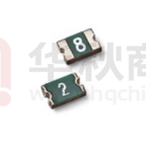
Surface Mount Devices
Lead free device
Size 5045mm/2018mils
Surface Mount packaging for automated assembly
Agency Approval:ROHS
Applications
Almost anywhere there is a low voltage power supply, up to DC60V and a load to be protected, including:
Computer mother board, Modem.
Telecommunication equipments
Dimensions(2018)
Recommended Mounting Pad Layout
C
A
1.5±0.1
1.5±0.1
4.6±0.1
ZZZ
B
E
D
3.4±0.1
Dimensions in millimerters
C
B
A
D
E
Part Number
Min.
Max.
Min.
Max.
Min.
Max.
Min.
Min.
TSM030
4.72
5.44
4.22
4.93
0.60
1.10
0.30
0.25
TSM050
4.72
5.44
4.22
4.93
0.60
1.10
0.30
0.25
TSM100
4.72
5.44
4.22
4.93
0.45
0.80
0.30
0.25
TSM100/33
4.72
5.44
4.22
4.93
0.45
0.80
0.30
0.25
TSM150
4.72
5.44
4.22
4.93
0.45
0.80
0.30
0.25
TSM200
4.72
5.44
4.22
4.93
0.45
0.80
0.30
0.25
REV . 2017 . 05 . 12
www.spsemi.cn
Page 1 of 4
�SPSEMI
PPTC/TSM(2018) Series
� � � �
Electrical Characteristics (25 ℃ )
Maximum Time To Trip
Resistance
R1max.
Rmin
(Ω)
(Ω)
I hold
I trip
V max.
I max.
P d max.
(A)
(A)
(Vdc)
(A)
(W)
Current
(A)
Time
(Sec.)
TSM030
0.30
0.6
60
100
0.9
1.5
3.0
0.50
2.30
TSM050
0.55
1.2
60
100
1.0
2.5
3.0
0.20
1.00
TSM100
1.10
2.2
15
100
1.1
8.0
0.4
0.06
0.36
TSM100/33
1.10
2.2
33
100
1.1
8.0
0.4
0.06
0.36
TSM150
1.50
3.0
15
100
1.1
8.0
0.8
0.05
0.17
TSM200
2.00
4.0
10
100
1.1
8.0
2.4
0.03
0.10
Part Number
Notes :
I hold = Hold Current. Maximum current device will not trip in 25°C still air.
I trip = Trip Current. Minimum current at which the device will always trip in 25°C still air.
V max = Maximum operating voltage device can withstand without damage at rated current (Imax).
I max = Maximum fault current device can withstand without damage at rated voltage (Vmax).
P d = Power dissipation when device is in the tripped state in 25°C still air environment at rated voltage.
R min = Minimum device resistance prior to tripping at 25°C.
R 1 max = Maximum device resistance is measured one hour post reflow.
CAUTION : Operation beyond the specified ratings may result in damage and possible arcing and flame.
Thermal Derating Chart-I hold (A)
Maximum ambient operating temperature (Tmao)vs.hold current (Ihold)
Part Number
-40 °C
-20 °C
0 °C
25 °C
40 °C
50 °C
60 °C
70 °C
85 °C
TSM030
0.48
0.42
0.35
0.30
0.24
0.21
0.17
0.15
0.10
TSM050
0.87
0.77
0.67
0.55
0.46
0.41
0.36
0.31
0.23
TSM100
1.71
1.52
1.32
1.10
0.94
0.84
0.74
0.64
0.50
TSM100/33
1.71
1.52
1.32
1.10
0.94
0.84
0.74
0.64
0.50
TSM150
2.38
2.10
1.82
1.50
1.27
1.13
0.99
0.85
0.64
TSM200
2.95
2.65
2.35
2.00
1.74
1.59
1.44
1.29
1.06
REV . 2017 . 05 . 12
www.spsemi.cn
Page 2 of 4
�SPSEMI
PPTC/TSM(2018) Series
� � � �
Characteristic Curve
Typical Time To Trip At 25 °C
Thermal Derating Curve
100
B C
A
E
D
A : 0.30A
B : 0.55A
C : 1.10A
D : 1.50A
E : 2.00A
140
10
120
Time In Seconds
Percent of Derated Current-%
160
100
80
60
40
1
0.1
0.01
20
0
-40
-20
0
20
40
60
0.001
0.1
80
1
10
100
Current In Amperes
Temerature-℃
Environmental Specifications
Test
Conditions
Resistance Change
Passive aging
+85°C, 1000 hrs.
±5% typical
Humidity aging
+85°C, 85% R.H. , 168 hours
±5% typical
Thermal shock
+85°C to -40°C, 20 times
±33% typical
Resistance to solvent
MIL-STD-202,Method 215
No change
Vibration
MIL-STD-202,Method 201
No change
Ambient operating conditions : - 40 °C to +85 °C
Maximum surface temperature of the device in the tripped state is 125 °C
Termination Pad Characteristics
Terminal pad materials
Tin-Plated Nickle-Copper or Gold-Plated Nickle-Copper
Terminal pad solderability
Meets EIA specification RS186-9E and ANSI/J-STD-002 Category 3.
REV . 2017 . 05 . 12
www.spsemi.cn
Page 3 of 4
�SPSEMI
PPTC/TSM(2018) Series
� � � �
Recommended Soldering Conditions
Recommended Conditions
Reflow Soldering
Pb-Free assembly
Profile Feature
tP
TP
+150℃
-Temperature Max(T s(max) )
+200℃
-Time(Min to Max)(t s )
60-180seconds
Average ramp up rate
(T s(max) to T p )
Time maintained
above:
Critical Zone
T L to T P
Ramp-up
TL
tL
Temperature
Pre Heat
-Temperature Min(T s(min) )
3℃/second Max.
-Temperature(T L )
+217℃
-Time(t L )
60-150seconds
Peak Temp(T P )
+260(+0/-5)℃
Time within 5℃ of actual Peak Temp(t p )
Ramp-down Rate
20-40seconds
Time 25℃ to Peak Temp(T P )
8 minutes Max.
T s (max)
Ramp-down
Preheat
T s (min)
ts
25
6℃/second Max.
time to peak temperature
(t 25℃ to peak)
Time
Recommended reflow methods: I R , vapor phase oven, hot air oven, N 2 environment for lead-free.
Devices are not designed to be wave soldered to the bottom side of the board.
Recommended maximum paste thickness is 0.25mm (0.010inch).
Devices can be cleaned using standard industry methods and solvents.
Notes:
If reflow temperatures exceed the recommended profile, devices may not meet the performance requirements.
Packageing Information
Part Number
Packaging Option
Quantity
TSM030-050
Reel
1500pcs/reel
TSM100-200
Reel
2500pcs/reel
REV . 2017 . 05 . 12
www.spsemi.cn
Page 4 of 4
�
很抱歉,暂时无法提供与“TSM050”相匹配的价格&库存,您可以联系我们找货
免费人工找货- 国内价格
- 1+0.85400
- 30+0.82350
- 100+0.79300
- 500+0.73200
- 1000+0.70150
- 2000+0.68320


 工商网监
湘ICP备2023018690号
工商网监
湘ICP备2023018690号
