Standard Pressure Ranges ................................ 2
Pressure Sensor Maximum Ratings................... 2
Environmental Specifications ........................... 2
Electrical Block Diagram ................................. 2
Performance Characteristics ............................ 3
I2C / SPI Electrical Parameters ......................... 4
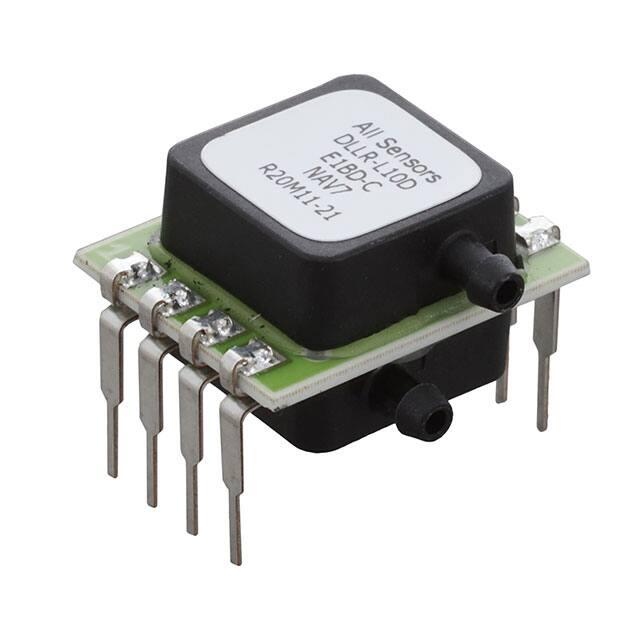
Device Ordering Options ................................ 5
Operation Overview ..................................... 6-7
Digital Interface Command Formats ................ 8
Digital Interface Data Format .......................... 9
The digital interface eases integration of the sensors into a
wide range of process control and measurement systems,
allowing direct connection to serial communications channels. For battery-powered systems, the sensors can enter very
low-power mode between readings to minimize load on the
power supply.
These calibrated and compensated sensors provide accurate,
stable output over a wide temperature range. This series
is intended for use with non-corrosive, non-ionic working
fluids such as air, dry gases.
https://www.allsensors.com/products/dllr-series
I2C Interface ............................................... 9-10
SPI Interface .................................................. 11
Interface Timing Diagrams ............................ 12
Extended Compensation Instructions ........ 13-15
How to Order Guide ..................................... 16
Dimensional Package Drawings
SIP ..................................................... 17-18
DIP .................................................... 19-20
SMT ........................................................ 21
Suggested Pad Layout .................................... 22
All Sensors
f 408 225 2079
Features & Applications ................................... 2
The DLLR Series Mini Digital Output Sensor is based on
All Sensors’ CoBeam2 TM Technology. This reduces package
stress susceptibility, resulting in improved overall long term
stability and vastly improves the position sensitivity.
a 16035 Vineyard Blvd. Morgan Hill, CA 95037
Table of Contents
p 408 225 4314
Introduction
e www.allsensors.com
all sensors
DLLR - High Accuracy Pressure Sensors Series
DS-0358 Rev A
Page 1
�Applications
• 10 & 30 inH2O Pressure Ranges
• 1.68V to 3.6V Supply Voltage Range
• I2C or SPI Interface (Automatically Selected)
• Better Than 0.10% Accuracy
• High Resolution 16/17/18 Bit Output
• Medical Breathing
• Environmental Controls
• HVAC
• Industrial Controls
• Portable/Hand-Held Equipment
Standard Pressure Ranges
Operating Range
Proof Pressure
A
Burst Pressure
Nominal Span
Pa
inH2O
kPa
inH2O
kPa
Counts
± 10
2488.4
100
25
300
75
±0.4 * 224
DLLR-L10G
0 to 10
2488.4
100
25
300
75
0.8 * 224
DLLR-L30D
± 30
7465.2
100
25
300
75
±0.4 * 224
DLLR-L30G
0 to 30
7465.2
100
25
300
75
0.8 * 224
f 408 225 2079
inH2O
DLLR-L10D
Note A: Operating range in Pa is expressed as an approximate value.
Supply Voltage (Vs)
3.63 Vdc
Common Mode Pressure
10 psig
Lead Temperature (soldering 2-4 sec.)
270 °C
p 408 225 4314
Electrical Block Diagram
Pressure Sensor Maximum Ratings
For SIP Packages
Vs
SCL
I2C
SDA
Gnd
Environmental Specifications
Temperature Ranges
Compensated:
Operating
Storage
Commercial
For DIP and J-Lead Packages
0°C to 70°C
-25°C to 85 °C
-40°C to 125 °C
Humidity Limits (non condensing)
0 to 95% RH
SPI
Vs
SCLK
MISO
MOSI
/SS
EOC
Gnd
All Sensors
Vs
SCL
- OR -
I2C
SDA
EOC
Gnd
DS-0358 Rev A
Page 2
Table of Contents
a 16035 Vineyard Blvd. Morgan Hill, CA 95037
Device
e www.allsensors.com
Features
all sensors
DLLR Series High Accuracy Pressure Sensors
�Performance Characteristics for DLLR Series High Accuracy Low Pressure Sensors
All parameters are measured at ±3.3V ±5% excitation and 25C unless otherwise specified (Note 9). Pressure measurements are
with positive pressure applied to PORT B.
Parameter
Specification
Minimum
Typical
Maximum
Units
LxxD
-
±0.4 * 224
-
Dec Count
1
LxxG
-
0.8 * 224
-
Dec Count
1
LxxD
-
0.5 * 224
-
Dec Count
-
LxxG
-
0.1 * 2
24
-
Dec Count
-
-
±0.10
±6
±9
±0.03
±0.25
±0.10
%FSS
ppmFSS/C
ppmFSS/C
%FSS
2, 6
4, 6
4, 6
3, 6
-
±0.06
±7
±3
±0.03
±0.20
±0.10
%FSS
ppmFSS/C
ppmFSS/C
%FSS
2, 6
4, 6
4, 6
3, 6
-
±0.10
±10
±4
±0.03
±0.35
±0.10
%FSS
ppmFSS/C
ppmFSS/C
%FSS
2, 6
4, 6
4, 6
3, 6
-
±0.05
±6
±3
±0.03
±0.15
±0.10
%FSS
ppmFSS/C
ppmFSS/C
%FSS
2, 6
4, 6
4, 6
3, 6
Offset Position Sensitivity (±1g)
-
±0.10
-
%FSS
-
Offset Long Term Drift (one year)
-
±0.25
-
%FSS
-
Notes
Output Span
Offset Output @ Zero Diff. Pressure (OSdig)
Error Summary
L10D
Total Error Band
Span Temperature Shift
Offset Temperature Shift
Accuracy
L10G
Total Error Band
Span Temperature Shift
Offset Temperature Shift
Accuracy
L30D
Total Error Band
Span Temperature Shift
Offset Temperature Shift
Accuracy
L30G
Total Error Band
Span Temperature Shift
Offset Temperature Shift
Accuracy
Pressure Digital Resolution - No Missing Codes
16-bit Option
15.7
-
-
bit
-
17-bit Option
16.7
-
-
bit
-
18-bit Option
17.7
-
-
bit
-
Resolution
-
16
-
bit
-
Overall Accuracy
-
2
-
°C
-
During Active State (ICCActive)
-
2
2.6
mA
-
During Idle State (ICCIdle)
-
100
250
nA
-
-
-
2.5
ms
5
30
-
-
ms
10
Temperature Output
5, 7, 8
Supply Current Requirement
Power On Delay
Memory Read Access Time
Data Update Time (tDU)
(see table below)
5, 7
DLLR Series High Accuracy Digital Pressure Sensors
Table of Contents
Page 3
�I2C / SPI Electrical Parameters for DLLR
Symbol Min Typ Max Units Notes
Input High Level
-
80.0
-
100
% of Vs
5
Input Low Level
-
0
-
20.0
% of Vs
5
Output Low Level
-
-
-
10.0
% of Vs
5
I2C Pull-up Resistor
-
1000
-
-
I2C Load Capacitance on SDA, @ 400 kHz CSDA
-
-
200
pF
5
I2C Input Capacitance (each pin)
-
-
10.0
pF
5
Pressure Output Transfer Function
𝑃𝑃𝑃𝑃𝑃𝑃𝑃𝑃𝑑𝑑𝑑𝑑𝑑𝑑 − 𝑂𝑂𝑂𝑂𝑑𝑑𝑑𝑑𝑑𝑑
� × 𝐹𝐹𝐹𝐹𝐹𝐹(𝑖𝑖𝑖𝑖𝐻𝐻2 𝑂𝑂)
224
𝑃𝑃𝑃𝑃𝑃𝑃𝑃𝑃𝑑𝑑𝑑𝑑𝑑𝑑
Is the sensor 24-bit digital output, following corrections applied by extended
compensation.
𝑂𝑂𝑂𝑂𝑑𝑑𝑑𝑑𝑑𝑑
Is the specified digital offset
𝐹𝐹𝐹𝐹𝐹𝐹(𝑖𝑖𝑖𝑖𝐻𝐻2 𝑂𝑂)
For Gage Operating Range sensors:
For Differential Operating Range sensors:
24
0.1 * 2
24
0.5 * 2
f 408 225 2079
Where:
e www.allsensors.com
𝑃𝑃𝑃𝑃𝑃𝑃𝑃𝑃𝑃𝑃𝑃𝑃𝑃𝑃𝑃𝑃(𝑖𝑖𝑖𝑖𝐻𝐻2 𝑂𝑂) = 1.25 × �
The sensor Full Scale Span in inches H2O
For Gage Operating Range sensors:
For Differential Operating Range sensors:
Full Scale Pressure
2 x Full Scale Pressure
p 408 225 4314
Temperature Output Transfer Function
����������� ��� � �
������� ∗ 125
� � ��
2��
Where:
�������
The sensor 24‐bit digital temperature output.
(Note that only the upper 16 bits are significant)
Specification Notes
note
1: THE SPAN IS THE ALGEBRAIC DIFFERENCE BETWEEN FULL SCALE DECIMAL COUNTS AND THE OFFSET DECIMAL COUNTS. THE FULL SCALE PRESSURE IS THE
note
2: TOTAL ERROR BAND CONSISTS OF OFFSET AND SPAN TEMPERATURE AND CALIBRATION ERRORS, LINEARITY AND PRESSURE HYSTERESIS ERRORS, OFFSET
note
3: ACCURACY INCLUDES PRESSURE HYSTERESIS, REPEATABILITY AND BEST-FIT STRAIGHT LINE LINEARITY, EVALUATED AT 25C.
note
4: PARTS PER MILLION OF FULL-SCALE SPAN PER DEGREE C.
note
5: PARAMETER IS CHARACTERIZED AND NOT 100% TESTED.
note
6: EVALUATED FOLLOWING CORRECTIONS DESCRIBED IN EXTENDED COMPENSATION SECTION.
note
7: DATA UPDATE TIME IS EXCLUSIVE OF COMMUNICATIONS, FROM COMMAND RECEIVED TO END OF BUSY STATUS. THIS CAN BE OBSERVED AS EOC PIN
note
8: AVERAGE CURRENT CAN BE ESTIMATED AS : ICCIdle + (tDU / Reading Interval) * ICCActive). REFER TO FIGURE 2 FOR ACTIVE AND IDLE CONDITIONS OF THE
note
9: THE SENSOR IS CALIBRATED WITH A 3.3V SUPPLY HOWEVER, AN INTERNAL REGULATOR ALLOWS A SUPPLY VOLTAGE OF 1.68V TO 3.6V TO BE USED
note
10: DELAY BETWEEN END OF MEMORY READ REQUEST COMMUNICATION AND START OF MEMORY DATA READ COMMUNICATION.
MAXIMUM POSITIVE CALIBRATED PRESSURE.
WARM-UP SHIFT, OFFSET POSITION SENSITIVITY AND LONG TERM OFFSET DRIFT ERRORS.
LOW- STATE DURATION.
SENSOR (THE ACTIVE STATE IS WHILE EOC PIN IS LOW).
WITHOUT AFFECTING THE OVERALL SPECIFICATIONS. THIS ALLOWS DIRECT OPERATION FROM A BATTERY SUPPLY.
All Sensors
Table of Contents
all sensors
CI2C_IN
Ω 5
DS-0358 Rev A
Page 4
a 16035 Vineyard Blvd. Morgan Hill, CA 95037
Parameter
�Device Ordering Options
Output Resolution
Calibrated output resolution can be ordered to be 16, 17, or 18 bits.
Higher resolution results in slower update times; see the Data Update Time in the Performance Characteristics table.
DLLR Series High Accuracy Digital Pressure Sensors
Table of Contents
Page 5
�Operation Overview
The DLLR is a digital sensor with a signal path that includes a sensing element, a variable- bit analog to digital
converter, a DSP and an IO block that supports either an I2C or SPI interface (see Figure 1 below). The sensor also
includes an internal temperature reference and associated control logic to support the configured operating mode.
Since there is a single ADC, there is also a multiplexer at the front end of the ADC that selects the signal source for the
ADC.
Sensor Commands: Five Measurement commands are supported, returning values of either a single pressure /
temperature reading or an average of 2, 4, 8, or 16 readings. Each of these commands wakes the sensor from Idle state
into Active state, and starts a measurement cycle. For the Start-Average commands, this cycle is repeated the
appropriate numper of times, while the Start-Single command performs a single iteration. When the DSP has
completed calculations and the new values have been made available to the I/O block, the sensor returns to Idle state.
The sensor remains in this low-power state until another Measurement command is received.
After completion of the measurement, the result may then be read using the Data Read command. The ADC and DSP
remain in Idle state, and the I/O block returns the 7 bytes of status and measurement data. See Figure 2, following. At
any time, the host may request current device status with the Status Read command.
See Table 1 for a summary of all commands.
For optimum sensor performance, All Sensors recommends that Measurement commands be issued at a fixed interval
by the host system. Irregular request intervals may increase overall noise on the output.
Furthermore, if reading intervals are much slower than the Device Update Time, using the Averaging commands is
suggested to reduce offset shift. This shift is constant with respect to time interval, and may be removed by the application. For longer fixed reading intervals, this shift may be removed by the factory on special request.
I/O Interface Configuration: The sensor automatically selects SPI or I2C serial interface, based on the following protocol: If the /SS input is set low by the host (as occurs during a SPI command transaction), the I/O interface will remain
configured for SPI communications until power is removed. Otherwise, once a valid device address and command
have been received over the I2C interface, the I/O interface will remain configured for I2C until power is removed.
NOTE: The four-pin (SIP) packages only support the I2C interface.
All Sensors
Table of Contents
DS-0358 Rev A
Page 6
f 408 225 2079
p 408 225 4314
The DSP receives the converted pressure and temperature information and applies a multi-order transfer function to
compensate the pressure output. This transfer function includes compensation for span, offset, temperature effects on
span, temperature effects on offset and second order temperature effects on offset. There is also linearity compensation
for gage devices and front to back linearity compensation for differential devices. This compensated output is further
improved by applying additional external correction, as described later in the Extended Compensation instructions
section.
a 16035 Vineyard Blvd. Morgan Hill, CA 95037
The ADC performs conversions on the raw sensor signal (P), the temperature reference (T) and a zero reference (Z)
during the ADC measurement cycle.
e www.allsensors.com
all sensors
Figure 1 - DLLR Block Diagram
�Operation Overview
Figure 2 - DLLR Communication
Start-Single Command
Command
Start-Single
Internal State
Idle
Interal Operation
Idle
Data Read
Active
Start-Single
Idle
ADC (Temp, Zero, Pressure)
Idle
DSP
Idle
Active
ADC (Temp, Zero, Pressure)
Idle
DSP
New Data Available
EOC
Start-Average2 / 4 / 8 / 16 Commands (Auto Averaging)
Command
Data Read
Start-Average2/ 4/ 8/ 16
Internal State
Idle
Interal Operation
Idle
Active
ADC (Temp, Zero, Pressure) 1
ADC (Temp, Zero, Pressure) n
DSP
Start-Average2/ 4/ 8/ 16
Idle
Active
Idle
ADC (T, Z, P)…
New Data Available
EOC
Digital Interface Command Formats
When requesting the start of a measurement, the command length for I2C is 1 byte, for SPI it is 3 bytes.
When requesting sensor status over I2C, the host simply performs a 1-byte read transfer.
When requesting sensor status over SPI, the host must send the Status Read command byte while reading 1 byte.
When reading sensor data over I2C, the host simply performs a 7-byte read transfer.
When reading sensor data over SPI, the host must send the 7-byte Data Read command while reading the data.
SENDING UNDOCUMENTED COMMANDS TO SENSOR WILL CORRUPT CALIBRATION AND IS NOT COVERED
BY WARRANTY.
Table 1 - DLLR Sensor Command Set
Measurement Commands
Description
SPI ( 3 bytes )
I2C ( 1 byte)
Start-Single
0xAA
0x00
0x00
0xAA
Start-Average2
0xAC
0x00
0x00
0xAC
Start-Average4
0xAD
0x00
0x00
0xAD
Start-Average8
0xAE
0x00
0x00
0xAE
Start-Average16
0xAF
0x00
0x00
0xAF
Read Sensor Data
I2C Read of 7 bytes from device
Read of 7 bytes from device
SPI Host must send [0xF0], then 6 bytes of [0x00] on MOSI
Sensor Returns 7 bytes on MISO
Read Sensor Status
I2C Read of 1 byte from device.
Read of 1 byte from device
SPI Host must send [0xF0] on MOSI
Sensor Returns 1 byte on MISO
DLLR Series High Accuracy Digital Pressure Sensors
Table of Contents
Page 7
�Digital Interface Command Formats
The Memory Read Command is used to retrieve the extended Compensation Coefficients from internal memory of the
sensor. Values (A, B, C, and D) are 32-bit signed integers, stored in eight 16-bit registers at addresses 47 through 54.
Values TC50H and TC50L are stored in high byte and low byte, respectively, of address 55, as signed 8-bit integers.
Value E is an 8-bit signed integer, stored at High Byte of address 56.
49 (0x31)
[BHW]
50 (0x32)
[BLW]
51 (0x33)
[CHW]
52 (0x34)
[CLW]
53 (0x35)
[DHW]
54 (0x36)
[DLW]
55 (0x37)
[TC50H]
[TC50L]
56 (0x38)
[E]
Each Word is stored in form ([High Byte]:[Low Byte]).
To form the complete integers A, B, C, and D, assemble the words in order ([xHW] : [xLW]). For E, the 8-bit high
byte represents the complete integer. For TC50H and TC50L, the high byte and low byte, respectively, represent the
complete integers.
The sequence of commands to retrieve these values is in the form of a Memory Read Request (See Table 3) followed
by a Memory Data Read ( See Table 4). Note that the Memory Read Access Time delay must be observed between the
request and the read operations.
Table 3 - Memory Read Request Command
Description
Read Request
Memory Commands: I2C Write or SPI MOSI:
SPI ( 3 bytes )
0x00 0x00
(Values 47 -56 only )
I2C (1 byte)
(Values 47 -56 only )
It must be emphasized that these commands be used accurately and carefully. Errors in forming or transmitting these
commands can result in degraded sensor operation.
Table 4 - Memory Data Read Operation
a 16035 Vineyard Blvd. Morgan Hill, CA 95037
Read Memory Data
I2C Read of 3 bytes from device.
Read of 3 bytes from device.
SPI Host must send [0xF0], then 2 bytes of [0x00] on MOSI.
Sensor returns 3 bytes on MISO.
Example : I2C Read of Coefficient B :
Write , and read back: .
Write , and read back: .
B = [BHW:BLW], assembling BHW and BLW into a signed 32-bit integer.
Example : SPI Read of Coefficient D :
Write ,
Set output buffer to , then perform 3-byte transfer.
Input buffer will then contain: < DHW(high byte)> < DHW(low byte)>.
Write ,
Set output buffer to , then perform 3-byte transfer.
Input buffer will then contain: < DLW(high byte)> < DLW(low byte)>.
D = [DHW:DLW], assembling DHW and DLW into a signed 32-bit integer.
All Sensors
Table of Contents
e www.allsensors.com
48 (0x30)
[ALW]
f 408 225 2079
47 (0x2F)
[AHW]
p 408 225 4314
Address
Coeff. Word
all sensors
Table 2 - Coefficient Memory Map
DS-0358 Rev A
Page 8
�Digital Interface Data Format
For either type of digital interface, the format of data returned from the sensor is the same. For measurement data, the
first byte consists of the Status Byte followed by a 24-bit unsigned pressure value and a 24-bit unsigned temperature
value. See the Pressure Output Transfer Function and Temperature Output Transfer Function definitions on page 3
for converting to pressure and temperature. Refer to ‘Extended Compensation Instructions Section’ for improving the
accuracy of output pressure values.
For memory data output, the status byte is followed by the high byte, then low byte of the memory word.
Refer to Table 5 for the overall data format of the sensor. Table 6 shows the Status Byte definition.
Note that a completed reading without error will return status 0x40.
Table 5 - Measurement Output Data Format
S[7:0]
Status
Byte
P[23:16]
Pressure
Byte 3
P[15:8]
Pressure
Byte 1
P[7:0]
Pressure
Byte 0
T[23:16]
Temperature
Byte 3
T[15:8]
Temperature
Byte 1
T[7:0]
Temperature
Byte 0
Table 6 - Memory Data Output Format
S[7:0]
Status
Byte
MEM [15:8]
MEM
High Byte
MEM[7:0]
MEM
Low Byte
Table 7- Status Byte Definition
Bit
Bit 7 [MSB]
6
5
4:3
2
1
Bit 0 [LSB]
Description
[Always = 0]
Power : [1 = Power On]
Busy: [ 1 = Processing Command, 0 = Ready]
Mode: [00 = Normal Operation ]
Memory Error [ 1 = EEPROM Checksum Fail]
Sensor Configuration [ always = 0]
ALU Error [1 = Error]
I2C Interface
I2C Command Sequence
The part enters Idle state after power-up, and waits for a command from the bus master. Any of the five
Measurement commands may be sent, as shown in Table 1. Following receipt of one of these command bytes,
the EOC pin is set to Low level, and the sensor Busy bit is set in the Status Byte. After completion of measurement
and calculation in the Active state, compensated data is written to the output registers, the EOC pin is set high,
and the processing core goes back to Idle state. The host processor can then perform the Data Read operation,
which for I2C is simply a 7-byte Device Read.
If the EOC pin is not monitored, the host can poll the Status Byte by repeating the Status Read command, which
for I2C is a one-byte Device Read. When the Busy bit in the Status byte is zero, this indicate that valid data is
ready, and a full Data Read of all 7 bytes may be performed.
DO NOT SEND COMMANDS TO SENSOR OTHER THAN THOSE DEFINED IN TABLES 1, 3 & 4.
DLLR Series High Accuracy Digital Pressure Sensors
Table of Contents
Page 9
�I2C Interface (Cont’d)
I2C Bus Communications Overview
The I2C interface uses a set of signal sequences for communication. The following is a description of the supported sequences and their associated mnemonics. Refer to Figure 3 for the associated usage of the following
signal sequences.
all sensors
Bus not Busy (I): During idle periods both data line (SDA) and clock line (SCL) remain HIGH.
START condition (ST): A HIGH to LOW transition of SDA line while the clock (SCL) is HIGH is interpreted as
START condition. START conditions are always set by the master. Each initial request for a pressure value has to
begin with a START condition.
Slave address (An): The I2C-bus requires a unique address for each device. The DLLR sensor has a preconfigured slave address (defined by device option, see Table 9). After setting a START condition the master sends
the address byte containing the 7 bit sensor address followed by a data direction bit (R/W). A “0” indicates a
transmission from master to slave (WRITE), a “1” indicates a device-to master request (READ).
e www.allsensors.com
Acknowledge (A or N): Data is transferred in units of 8 bits (1 byte) at a time, MSB first. Each data-receiving
device, whether master or slave, is required to pull the data line LOW to acknowledge receipt of the data. The
Master must generate an extra clock pulse for this purpose. If the receiver does not pull the data line down, a
NACK condition exists, and the slave transmitter becomes inactive. The master determines whether to send
the last command again or to set the STOP condition, ending the transfer.
f 408 225 2079
DATA valid (Dn): State of data line represents valid data when, after a START condition, data line is stable for
duration of HIGH period of clock signal. Data on line must be changed during LOW period of clock signal.
There is one clock pulse per data bit.
STOP condition (P): LOW to HIGH transition of the SDA line while clock (SCL) is HIGH indicates a STOP condition. STOP conditions are always generated by the master.
1. Measurement Commands: Start-Single ( to start reading of single sample):
Start-Single
C7…C0: 0xAA
Start-Average2
C7…C0: 0xAC
Start-Average4
C7…C0: 0xAD
Start-Average8
C7…C0: 0xAE
Start-Average16
C7…C0: 0xAF
Set by bus master:
Set by sensor:
I
ST A6 A5 A4 A3 A2 A1 A0 W
I
ST A6 A5 A4 A3 A2 A1 A0 R
I
ST A6 A5 A4 A3 A2 A1 A0 R
A
C7 …
C0
N
SP
I
SP
I
2. Status Read:
Set by bus master:
Set by sensor:
A S7 … S0
N
3. Data Read:
Set by bus master:
Set by sensor:
Bus states:
Idle:
Start:
Stop:
Ack:
Nack:
“Read” bit (1):
“Write” bit (0):
I
ST
SP
A
N
R
W
Sensor Address:
A6 … A0
A S7 … S0
A
A
P23 … P16
A
P15 … P8
A
P7 … P0
A
T23 … T16
A
T15 … T8
N SP
T7 … T0
Data bits:
Status:
Pressure data:
Temperature data:
S7 … S0
P23 … P0
T23 … T0
Command Bits:
C7 … C0
All Sensors
DS-0358 Rev A
Page 10
Table of Contents
I
a 16035 Vineyard Blvd. Morgan Hill, CA 95037
p 408 225 4314
Figure 3 - I2C Communication Diagram
�SPI Interface
SPI Command Sequence
As with the I2C interface configuration, the part enters Idle state after power-up, and waits for a command from the
SPI master. To start a measurement cycle, one of the 3- byte Measurement Commands (see Table 1) must be issued
by the master. To start a memory read operation, the memory read request (see Table 3) must be sent.
The data returned by the sensor during this command request consists of the Status Byte followed by two undefined
data bytes.
On successful decode of a measurement command, the EOC pin is set Low as the core goes into Active state for
measurement and calculation. When complete, updated sensor data is written to the output registers, and the core
goes back to the Idle state. The EOC pin is set to a High level at this point, and the Busy status bit is set to 0. At
any point during the Active or Idle periods, the SPI master can request the Status Byte by sending a Status Read command (a single byte with value 0xF0).
As with the I2C configuration, a Busy bit of value 0 in the Status Byte or a high level on the EOC pin indicates that
a valid data set may be read from the sensor. The Data Read command must be sent from the SPI master (The first
byte of value 0xF0 followed by 6 bytes of 0x00). For memory read operations, see Table 4 for reading back the
result.
NOTE: Sending commands that are not defined in Tables 1, 3, or 4 will corrupt sensor operation.
SPI Bus Communications Overview
The sequence of bits and bus signals are shown in the following illustration (Figure 4). Refer to Figure 5 in the Interface Timing Diagram section for detailed timing data.
Figure 4 - SPI Communications Diagram
Measurement or Memory Read Command
SCLK
--First Command Byte (0xAA / 0xAC / 0xAD / 0xAE / 0xAF)
MOSI
XXXX
C23
C22
C21
MISO HI-Z
S7
S6
S5
Lower Command Bytes (0x00 0x00)
C20
C19
C18
C17
C16
C 15
S4
S3
S2
S1
S0
XX
-----
S7 … S0 (Status)
C1
C0
XXXX
XX
XX
HI-Z
(Undefined Data)
SS
---
Read Status Command
SCLK
Command (0xF0)
MOSI Don't Care
1
1
1
MISO
S7
S6
S5
Hi-Z
1
0
0
0
0
S4
S3
S2
S1
S0
Don't care
Hi-Z
S7 … S0 (Status)
SS
Measurement Data Read Command
SCLK
---
---
Command (0xF0 then 6 bytes of 0x00)
MOSI
Don't Care
1
1
1
1
0
0
0
0
MISO
Hi-Z
S7
S6
S5
S4
S3
S2
S1
S0
S7 … S0 (Status)
SS
0
0
P23 P22
---
0
0
---
P1
P0
0
0
T23 T22
---
0
0
Don't Care
---
T1
T0
Hi-Z
P23…P0 (Pressure)
T23…T0 (Temperature)
---
---
DLLR Series High Accuracy Digital Pressure Sensors
Page 11
Table of Contents
�Interface Timing Diagrams
Figure 5 - SPI Timing Diagram
tSSCLK
tLOW
tCLKD
tHIGH
SCLK
MOSI
(HI•Z)
(HI•Z)
all sensors
MISO
don't care
(don't
care)
tSSSO
tDSU
tDH
SS
tSSZ
tCLKSS
MIN
0.05
120
-8
100
100
50
50
0
-250
TYP
-
MAX
5
20
32
20
-
UNITS
MHz
ns
ns
ns
ns
ns
ns
ns
ns
ns
ns
e www.allsensors.com
SYMBOL
fSCLK
tSSCLK
tSSSO
tCLKD
tLOW
tHIGH
tDSU
tDH
tCLKSS
tSSZ
tIDLE
f 408 225 2079
PARAMETER
SCLK frequency (1)
SS low to first clock edge
SS low to serial out
Clock to data out
SCLK low width
SCLK high width
Data setup to clock
Data hold after clock
Last clock to rising SS
SS high to output hi-Z
Bus idle time
tIDLE
(1) Maximum by design, tested to 1.0 MHz.
tH STA
tHIGH
p 408 225 4314
Figure 6 - I2C Timing Diagram
tLOW
SCL
tSUS TA
PARAMETER
SCL frequency
SCL low width
SCL high width
Start condition setup
Start condition hold
Data setup to clock
Data hold to clock
Stop condition setup
Bus idle time
All Sensors
tSUDAT
SYMBOL
fSCL
tLOW
tHIGH
tSUSTA
tHSTA
tSUDAT
tHDAT
tSUSTP
tIDLE
tH DAT
MIN
100
1.3
0.6
0.6
0.6
0.1
0
0.6
2.0
tSUS TP
TYP
-
a 16035 Vineyard Blvd. Morgan Hill, CA 95037
SDA
tIDLE
MAX
400
-
UNITS
KHz
us
us
us
us
us
us
us
us
DS-0358 Rev A
Page 12
Table of Contents
�Extended Compensation Instructions
DLLR Series sensors have internal memory locations containing extended compensation coefficients.
For optimal accuracy of pressure readings, system designers can use these values to apply an additional
3rd-order error-correction adjustment to data delivered from the sensor, as well as additional temperature
compensation.
The four linearity coefficients are obtained for each sensor at the factory by a 3rd order minimization solution
to
Error = Pref - ( POut + f(POut) ), where
Pref is the true pressure applied;
POut is the sensor output;
f(POut) is a cubic correction function, Ax3+Bx2+Cx+D.
For improved accuracy over temperature, residual temperature dependent errors are minimized by the term:
TCadj = (1 - (E * 1.25 * | 0.5 - P |)) * (T - Tref) * TC50
where:
TC50 = TC50H for T > Tref
TC50 = TC50L for T ≤ Tref
On system startup:
Read the seven coefficients (A, B, C, D, E, TC50H, & TC50L) from sensor EEPROM, using the command sequence described in the datasheet section ‘Digital Interface Command Formats’.
A, B, C & D are 32-bit signed integers, representing a scaled magnitude from -1.0 to +1.0.
E, TC50H, & TC50L are 8-bit signed integers, representing a scaled magnitude from -1.0 to +1.0.
Example:
// I2C Input, output buffers:
unsigned char inbuf[32] = {0}, outbuf[32] = {0};
// ----- DLLR Coefficients -----float DLLR_A = 0.0, DLLR_B = 0.0, DLLR_C = 0.0, DLLR_D = 0.0;
float DLLR_E = 0.0, TC50H = 0.0, TCH50L = 0.0;
int32_t i32A = 0, i32B =0, i32C =0, i32D=0,
int8_t i8E = 0, i8TC50H = 0, i8TC50L = 0;
After sensor power-on:
outbuf[0] = 47;
// Address of A high word
success = DUT_I2C_Write(ui8Address, outbuf, 1); // 1-byte request
Wait_ms(20); // EEPROM access time : returns [Status][MSB][LSB]
success = DUT_I2C_Read(ui8Address, inbuf, 3); // EEPROM result
i32A = (inbuf[1]


 工商网监
湘ICP备2023018690号
工商网监
湘ICP备2023018690号

