Important notice
Dear Customer,
On 7 February 2017 the former NXP Standard Product business became a new company with the
tradename Nexperia. Nexperia is an industry leading supplier of Discrete, Logic and PowerMOS
semiconductors with its focus on the automotive, industrial, computing, consumer and wearable
application markets
In data sheets and application notes which still contain NXP or Philips Semiconductors references, use
the references to Nexperia, as shown below.
Instead of http://www.nxp.com, http://www.philips.com/ or http://www.semiconductors.philips.com/,
use http://www.nexperia.com
Instead of sales.addresses@www.nxp.com or sales.addresses@www.semiconductors.philips.com, use
salesaddresses@nexperia.com (email)
Replace the copyright notice at the bottom of each page or elsewhere in the document, depending on
the version, as shown below:
- © NXP N.V. (year). All rights reserved or © Koninklijke Philips Electronics N.V. (year). All rights
reserved
Should be replaced with:
- © Nexperia B.V. (year). All rights reserved.
If you have any questions related to the data sheet, please contact our nearest sales office via e-mail
or telephone (details via salesaddresses@nexperia.com). Thank you for your cooperation and
understanding,
Kind regards,
Team Nexperia
�IP4302CX2/A
Low profile bidirectional low capacitance ESD protection
diode
Rev. 1 — 28 November 2011
Product data sheet
1. Product profile
1.1 General description
The IP4302CX2/A is a bidirectional diode which is designed to provide protection to
downstream components from ElectroStatic Discharge (ESD) voltages as high as 15 kV
contact discharge according to the IEC 61000-4-2 model, far exceeding standard level 4.
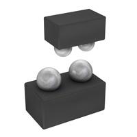
The device is fabricated using monolithic silicon technology and integrates one pair of
back-to-back diodes in a 0.4 mm pitch Wafer-Level Chip-Scale Package (WLCSP).
These features make the IP4302CX2/A ideal for use in applications requiring the utmost
in miniaturization such as mobile phone handsets, cordless telephones and other portable
electronic devices.
1.2 Features and benefits
Pb-free, RoHS compliant and free of halogen and antimony (Dark Green compliant)
Bidirectional ESD protection of one line
Integrated ESD protection withstanding 15 kV contact discharge, far exceeding
IEC 61000-4-2 level 4
Ultra low height of 0.40 mm only
0.52 mm 0.7 mm size package
1.3 Applications
Cellular handsets and accessories
Portable electronics
Subscriber Identity Module (SIM) card protection
Communication systems
Computers and peripherals
�IP4302CX2/A
NXP Semiconductors
Low profile bidirectional ESD protection diode
1.4 Quick reference data
Table 1.
Quick reference data
Tamb = 25 C; unless otherwise specified.
Symbol
Parameter
Conditions
Min
Typ
Max
Unit
VBR
breakdown voltage
IR = 1 mA
14.0
16.5
-
V
IR = 1 mA
-
16.5
14.0
V
Cd
diode capacitance
f = 1 MHz; VR = 0 V
-
-
10
pF
VESD
electrostatic discharge
voltage
contact discharge
15
-
+15
kV
[1][2]
[1]
Device is qualified with 1000 pulses of 15 kV contact discharges each, according to the IEC 61000-4-2
model and far exceeds the specified level 4 (8 kV contact discharge).
[2]
A special robust test is performed stressing the devices with 1000 contact discharges according to the
IEC 61000-4-2 model and far exceeds the specified level 4 (8 kV contact discharge).
2. Pinning information
Table 2.
Pin
Pinning
Description
Simplified outline
1
cathode (diode 1)
2
cathode (diode 2)
Graphic symbol
[1]
1
2
006aab041
A1
A1
(1)
(2)
001aao233
[1]
The device is electrically and mechanically symmetrical. Thus no marking is needed.
3. Ordering information
Table 3.
Ordering information
Type number Package
Name
Description
IP4302CX2/A WLCSP2 wafer level chip-size package; 2 bumps (A1-A1)
IP4302CX2_A
Product data sheet
All information provided in this document is subject to legal disclaimers.
Rev. 1 — 28 November 2011
Version
IP4302CX2/A
© NXP B.V. 2011. All rights reserved.
2 of 10
�IP4302CX2/A
NXP Semiconductors
Low profile bidirectional ESD protection diode
4. Limiting values
Table 4.
Limiting values
In accordance with the Absolute Maximum Rating System (IEC 60134).
Symbol Parameter
VESD
Conditions
electrostatic
discharge voltage
Min
Max
Unit
15
+15
kV
15
+15
kV
contact discharge
8
+8
kV
air discharge
15
+15
kV
[1][2]
contact discharge
air discharge
IEC 61000-4-2 level 4
4
+4
kV
Tj
junction temperature
-
150
C
Tamb
ambient temperature
35
+85
C
Tstg
storage temperature
65
+150
C
MIL-STD-883D (method 3015) HBM
[1]
Device is qualified with 1000 pulses of 15 kV contact discharges each, according to the IEC 61000-4-2
model and far exceeds the specified level 4 (8 kV contact discharge).
[2]
A special robust test is performed stressing the devices with 1000 contact discharges according to the
IEC 61000-4-2 model and far exceeds the specified level 4 (8 kV contact discharge).
5. Characteristics
Table 5.
Characteristics
Tamb = 25 C; unless otherwise specified.
Symbol Parameter
ILR
IP4302CX2_A
Product data sheet
reverse leakage current
Conditions
Min
Typ
Max
Unit
VRWM = 5 V
-
-
20
nA
VRWM = 5 V
20
-
-
nA
14.0
16.5
-
V
VBR
breakdown voltage
IR = 1 mA
IR = 1 mA
-
16.5 14.0 V
Cd
diode capacitance
f = 1 MHz; VR = 0 V
-
-
All information provided in this document is subject to legal disclaimers.
Rev. 1 — 28 November 2011
10
pF
© NXP B.V. 2011. All rights reserved.
3 of 10
�IP4302CX2/A
NXP Semiconductors
Low profile bidirectional ESD protection diode
IPP
−VCL −VBR −VRWM
IR
ILR
−ILR
−IR
VRWM VBR VCL
−
+
−IPP
008aaa270
Fig 1.
V-I characteristics for a bidirectional ESD protection diode
6. Application information
The IP4302CX2/A is designed for the protection of one bidirectional data or signal line
from the damage caused by ESD. The device may be used on lines where the signal
polarities are both, positive and negative with respect to ground.
line to be protected
DUT
GND
008aaa272
Fig 2.
Application diagram of IP4302CX2/A
6.1 Printed-Circuit Board (PCB) layout and protection device placement
PCB layout is critical for the suppression of ESD and Electric Fast Transient (EFT).
The following guidelines are recommended:
1. Place the device as close as possible to the input terminal or connector
2. The path length between the device and the protected line should be minimized
3. Keep parallel signal paths to a minimum
4. Avoid running protected conductors in parallel with unprotected conductors
5. Minimize all PCB conductive loops including power and ground loops
6. Minimize the length of the transient return path to ground
7. Avoid using shared transient return paths to a common ground point
IP4302CX2_A
Product data sheet
All information provided in this document is subject to legal disclaimers.
Rev. 1 — 28 November 2011
© NXP B.V. 2011. All rights reserved.
4 of 10
�IP4302CX2/A
NXP Semiconductors
Low profile bidirectional ESD protection diode
8. Ground planes should be used whenever possible; for multilayer PCBs use ground
vias
7. Package outline
WLCSP2: wafer level chip-size package; 2 bumps (A1-A1)
D
E
A
A2
A1
detail X
b1
A1
b
e
A1
X
European
projection
wlcsp2_a1-a1_po
Fig 3.
Table 6.
Package outline IP4302CX2/A (WLCSP2)
Dimensions for Figure 3
Symbol
Min
Typ
Max
Unit
A
0.37
0.40
0.43
mm
A1
0.05
0.06
0.07
mm
A2
0.32
0.34
0.36
mm
b
-
0.14
-
mm
b1
-
0.35
-
mm
D
0.49
0.52
0.55
mm
E
0.67
0.70
0.73
mm
e
-
0.4
-
mm
IP4302CX2_A
Product data sheet
All information provided in this document is subject to legal disclaimers.
Rev. 1 — 28 November 2011
© NXP B.V. 2011. All rights reserved.
5 of 10
�IP4302CX2/A
NXP Semiconductors
Low profile bidirectional ESD protection diode
8. Soldering
8.1 Reflow soldering recommendation
T
(°C)
Treflow(peak)
250
230
cooling rate
217
preheat
t1
t (s)
t2
t3
t4
t5
001aai943
The device is capable of withstanding at least three reflows with this profile.
Fig 4.
Pb-free solder reflow profile
Table 7.
IP4302CX2_A
Product data sheet
Characteristics
Symbol
Parameter
Treflow(peak)
peak reflow temperature
t1
time 1
t2
time 2
t3
t4
Min
Typ
Max
Unit
230
-
260
C
soak time
60
-
180
s
time during T 250 C
-
-
30
s
time 3
time during T 230 C
10
-
50
s
time 4
time during T > 217 C
30
-
150
s
t5
time 5
dT/dt
rate of change of
temperature
Conditions
-
-
540
s
cooling rate
-
-
6
C/s
preheat
2.5
-
4.0
C/s
All information provided in this document is subject to legal disclaimers.
Rev. 1 — 28 November 2011
© NXP B.V. 2011. All rights reserved.
6 of 10
�IP4302CX2/A
NXP Semiconductors
Low profile bidirectional ESD protection diode
9. Abbreviations
Table 8.
Abbreviations
Acronym
Description
DUT
Device Under Test
EFT
Electric Fast Transient
ESD
ElectroStatic Discharge
HBM
Human Body Model
PCB
Printed-Circuit Board
RoHS
Restriction of Hazardous Substances
SIM
Subscriber Identity Module
WLCSP
Wafer-Level Chip-Scale Package
10. Revision history
Table 9.
Revision history
Document ID
Release date
Data sheet status
Change notice
Supersedes
IP4302CX2_A v.1
20111128
Product data sheet
-
-
IP4302CX2_A
Product data sheet
All information provided in this document is subject to legal disclaimers.
Rev. 1 — 28 November 2011
© NXP B.V. 2011. All rights reserved.
7 of 10
�IP4302CX2/A
NXP Semiconductors
Low profile bidirectional ESD protection diode
11. Legal information
11.1
Data sheet status
Document status[1][2]
Product status[3]
Definition
Objective [short] data sheet
Development
This document contains data from the objective specification for product development.
Preliminary [short] data sheet
Qualification
This document contains data from the preliminary specification.
Product [short] data sheet
Production
This document contains the product specification.
[1]
Please consult the most recently issued document before initiating or completing a design.
[2]
The term ‘short data sheet’ is explained in section “Definitions”.
[3]
The product status of device(s) described in this document may have changed since this document was published and may differ in case of multiple devices. The latest product status
information is available on the Internet at URL http://www.nxp.com.
11.2
Definitions
Draft — The document is a draft version only. The content is still under
internal review and subject to formal approval, which may result in
modifications or additions. NXP Semiconductors does not give any
representations or warranties as to the accuracy or completeness of
information included herein and shall have no liability for the consequences of
use of such information.
Short data sheet — A short data sheet is an extract from a full data sheet
with the same product type number(s) and title. A short data sheet is intended
for quick reference only and should not be relied upon to contain detailed and
full information. For detailed and full information see the relevant full data
sheet, which is available on request via the local NXP Semiconductors sales
office. In case of any inconsistency or conflict with the short data sheet, the
full data sheet shall prevail.
Product specification — The information and data provided in a Product
data sheet shall define the specification of the product as agreed between
NXP Semiconductors and its customer, unless NXP Semiconductors and
customer have explicitly agreed otherwise in writing. In no event however,
shall an agreement be valid in which the NXP Semiconductors product is
deemed to offer functions and qualities beyond those described in the
Product data sheet.
11.3
Disclaimers
Limited warranty and liability — Information in this document is believed to
be accurate and reliable. However, NXP Semiconductors does not give any
representations or warranties, expressed or implied, as to the accuracy or
completeness of such information and shall have no liability for the
consequences of use of such information.
In no event shall NXP Semiconductors be liable for any indirect, incidental,
punitive, special or consequential damages (including - without limitation - lost
profits, lost savings, business interruption, costs related to the removal or
replacement of any products or rework charges) whether or not such
damages are based on tort (including negligence), warranty, breach of
contract or any other legal theory.
Notwithstanding any damages that customer might incur for any reason
whatsoever, NXP Semiconductors’ aggregate and cumulative liability towards
customer for the products described herein shall be limited in accordance
with the Terms and conditions of commercial sale of NXP Semiconductors.
malfunction of an NXP Semiconductors product can reasonably be expected
to result in personal injury, death or severe property or environmental
damage. NXP Semiconductors accepts no liability for inclusion and/or use of
NXP Semiconductors products in such equipment or applications and
therefore such inclusion and/or use is at the customer’s own risk.
Applications — Applications that are described herein for any of these
products are for illustrative purposes only. NXP Semiconductors makes no
representation or warranty that such applications will be suitable for the
specified use without further testing or modification.
Customers are responsible for the design and operation of their applications
and products using NXP Semiconductors products, and NXP Semiconductors
accepts no liability for any assistance with applications or customer product
design. It is customer’s sole responsibility to determine whether the NXP
Semiconductors product is suitable and fit for the customer’s applications and
products planned, as well as for the planned application and use of
customer’s third party customer(s). Customers should provide appropriate
design and operating safeguards to minimize the risks associated with their
applications and products.
NXP Semiconductors does not accept any liability related to any default,
damage, costs or problem which is based on any weakness or default in the
customer’s applications or products, or the application or use by customer’s
third party customer(s). Customer is responsible for doing all necessary
testing for the customer’s applications and products using NXP
Semiconductors products in order to avoid a default of the applications and
the products or of the application or use by customer’s third party
customer(s). NXP does not accept any liability in this respect.
Limiting values — Stress above one or more limiting values (as defined in
the Absolute Maximum Ratings System of IEC 60134) will cause permanent
damage to the device. Limiting values are stress ratings only and (proper)
operation of the device at these or any other conditions above those given in
the Recommended operating conditions section (if present) or the
Characteristics sections of this document is not warranted. Constant or
repeated exposure to limiting values will permanently and irreversibly affect
the quality and reliability of the device.
Terms and conditions of commercial sale — NXP Semiconductors
products are sold subject to the general terms and conditions of commercial
sale, as published at http://www.nxp.com/profile/terms, unless otherwise
agreed in a valid written individual agreement. In case an individual
agreement is concluded only the terms and conditions of the respective
agreement shall apply. NXP Semiconductors hereby expressly objects to
applying the customer’s general terms and conditions with regard to the
purchase of NXP Semiconductors products by customer.
Right to make changes — NXP Semiconductors reserves the right to make
changes to information published in this document, including without
limitation specifications and product descriptions, at any time and without
notice. This document supersedes and replaces all information supplied prior
to the publication hereof.
No offer to sell or license — Nothing in this document may be interpreted or
construed as an offer to sell products that is open for acceptance or the grant,
conveyance or implication of any license under any copyrights, patents or
other industrial or intellectual property rights.
Suitability for use — NXP Semiconductors products are not designed,
authorized or warranted to be suitable for use in life support, life-critical or
safety-critical systems or equipment, nor in applications where failure or
Export control — This document as well as the item(s) described herein
may be subject to export control regulations. Export might require a prior
authorization from competent authorities.
IP4302CX2_A
Product data sheet
All information provided in this document is subject to legal disclaimers.
Rev. 1 — 28 November 2011
© NXP B.V. 2011. All rights reserved.
8 of 10
�IP4302CX2/A
NXP Semiconductors
Low profile bidirectional ESD protection diode
Quick reference data — The Quick reference data is an extract of the
product data given in the Limiting values and Characteristics sections of this
document, and as such is not complete, exhaustive or legally binding.
Non-automotive qualified products — Unless this data sheet expressly
states that this specific NXP Semiconductors product is automotive qualified,
the product is not suitable for automotive use. It is neither qualified nor tested
in accordance with automotive testing or application requirements. NXP
Semiconductors accepts no liability for inclusion and/or use of
non-automotive qualified products in automotive equipment or applications.
In the event that customer uses the product for design-in and use in
automotive applications to automotive specifications and standards, customer
(a) shall use the product without NXP Semiconductors’ warranty of the
product for such automotive applications, use and specifications, and (b)
whenever customer uses the product for automotive applications beyond
NXP Semiconductors’ specifications such use shall be solely at customer’s
own risk, and (c) customer fully indemnifies NXP Semiconductors for any
liability, damages or failed product claims resulting from customer design and
use of the product for automotive applications beyond NXP Semiconductors’
standard warranty and NXP Semiconductors’ product specifications.
ESD protection devices — These products are only intended for protection
against ElectroStatic Discharge (ESD) pulses and are not intended for any
other usage including, without limitation, voltage regulation applications. NXP
Semiconductors accepts no liability for use in such applications and therefore
such use is at the customer’s own risk.
11.4
Trademarks
Notice: All referenced brands, product names, service names and trademarks
are the property of their respective owners.
12. Contact information
For more information, please visit: http://www.nxp.com
For sales office addresses, please send an email to: salesaddresses@nxp.com
IP4302CX2_A
Product data sheet
All information provided in this document is subject to legal disclaimers.
Rev. 1 — 28 November 2011
© NXP B.V. 2011. All rights reserved.
9 of 10
�IP4302CX2/A
NXP Semiconductors
Low profile bidirectional ESD protection diode
13. Contents
1
1.1
1.2
1.3
1.4
2
3
4
5
6
6.1
7
8
8.1
9
10
11
11.1
11.2
11.3
11.4
12
13
Product profile . . . . . . . . . . . . . . . . . . . . . . . . . . 1
General description . . . . . . . . . . . . . . . . . . . . . 1
Features and benefits . . . . . . . . . . . . . . . . . . . . 1
Applications . . . . . . . . . . . . . . . . . . . . . . . . . . . 1
Quick reference data . . . . . . . . . . . . . . . . . . . . 2
Pinning information . . . . . . . . . . . . . . . . . . . . . . 2
Ordering information . . . . . . . . . . . . . . . . . . . . . 2
Limiting values. . . . . . . . . . . . . . . . . . . . . . . . . . 3
Characteristics . . . . . . . . . . . . . . . . . . . . . . . . . . 3
Application information. . . . . . . . . . . . . . . . . . . 4
Printed-Circuit Board (PCB) layout
and protection device placement . . . . . . . . . . . 4
Package outline . . . . . . . . . . . . . . . . . . . . . . . . . 5
Soldering . . . . . . . . . . . . . . . . . . . . . . . . . . . . . . 6
Reflow soldering recommendation . . . . . . . . . . 6
Abbreviations . . . . . . . . . . . . . . . . . . . . . . . . . . . 7
Revision history . . . . . . . . . . . . . . . . . . . . . . . . . 7
Legal information. . . . . . . . . . . . . . . . . . . . . . . . 8
Data sheet status . . . . . . . . . . . . . . . . . . . . . . . 8
Definitions . . . . . . . . . . . . . . . . . . . . . . . . . . . . . 8
Disclaimers . . . . . . . . . . . . . . . . . . . . . . . . . . . . 8
Trademarks. . . . . . . . . . . . . . . . . . . . . . . . . . . . 9
Contact information. . . . . . . . . . . . . . . . . . . . . . 9
Contents . . . . . . . . . . . . . . . . . . . . . . . . . . . . . . 10
Please be aware that important notices concerning this document and the product(s)
described herein, have been included in section ‘Legal information’.
© NXP B.V. 2011.
All rights reserved.
For more information, please visit: http://www.nxp.com
For sales office addresses, please send an email to: salesaddresses@nxp.com
Date of release: 28 November 2011
Document identifier: IP4302CX2_A
�


 工商网监
湘ICP备2023018690号
工商网监
湘ICP备2023018690号
