MUSES8820
High Quality Audio
Dual Operational Amplifier
■ GENERAL DESCRIPTION
■ PACKAGE OUTLINE
The MUSES8820 is a high quality audio operational amplifier, which
is optimized for high-end audio and professional audio applications.
It is the best for audio preamplifiers, active filters, and line amplifiers
with excellent sound.
■ FEATURES
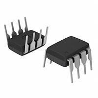
MUSES8820D
MUSES8820E
(DIP8)
(SOP8)
Vopr = ±3.5V to ±16V
4.5nV/√Hz at f=1kHz
0.3mV typ. 3mV max.
100nA typ. 500nA max. at Ta=25°C
110dB typ.
5V/µs typ.
●Operating Voltage
●Output noise
●Input Offset Voltage
●Input Bias Current
●Voltage Gain
●Slew Rate
●Bipolar Technology
●Package Outline
DIP8, SOP8 JEDEC 150mil
■ PIN CONFIGURATION
PIN FUNCTION
8
1
2
3
4
7
-+
+ -
6
5
1. A OUTPUT
2. A -INPUT
3. A +INPUT
4. V5. B +INPUT
6. B -INPUT
7. B OUTPUT
8.V+
MUSES and this logo are trademarks of New Japan Radio Co., Ltd.
Ver.2012-05-14
-1-
�MUSES8820
■ ABSOLUTE MAXIMUM RATINGS (Ta=25°C)
PARAMETER
SYMBOL
+
RATING
UNIT
-
Supply Voltage
V /V
±18
V
Common Mode Input Voltage
VICM
±15 (Note1)
V
Differential Input Voltage
VID
±30
V
Power Dissipation
PD
Output Current
IO
±50
mA
Operating Temperature Range
T opr
-40 to +85
°C
Storage Temperature Range
T stg
-50 to +150
°C
DIP8 : 870
SOP8 : 900(Note2)
mW
(Note1) For supply Voltages less than ±15 V, the maximum input voltage is equal to the Supply Voltage.
(Note2) Mounted on the EIA/JEDEC standard board (114.3×76.2×1.6mm, two layer, FR-4).
■ RECOMMENDED OPERATING CONDITION (Ta=25°C)
PARAMETER
Supply Voltage
SYMBOL
+
TEST CONDITION
MIN.
TYP.
MAX.
UNIT
-
±3.5
-
±16
V
MIN.
TYP.
MAX.
UNIT
-
V /V
■ ELECTRIC CHARACTERISTICS
DC CHARACTERISTICS (V+/V-=±15V, Ta=25°C unless otherwise specified)
PARAMETER
SYMBOL
TEST CONDITION
Operating Current
I cc
No Signal, R L =∞
-
8.0
12.0
mA
Input Offset Voltage
V IO
Rs≤10kΩ (Note3, 4)
-
0.3
3.0
mV
Input Bias Current
IB
(Note3, 4)
-
100
500
nA
Input Offset Current
I IO
(Note3, 4)
-
5
200
nA
Voltage Gain
AV
R L ≥2kΩ, V o =±10V
Rs≤10kΩ
90
110
-
dB
Common Mode Rejection Ratio
CMR
V ICM =±12V (Note5)
Rs≤10kΩ
80
110
-
dB
Supply Voltage Rejection Ratio
SVR
V /V =±3.5 to ±16.0V
Rs≤10kΩ (Note3, 6)
80
110
-
dB
Max Output Voltage
V OM
R L =2kΩ
±12
±13.5
-
V
Input Common Mode Voltage
Range
V ICM
CMR≥80dB
±12
±13.5
-
V
+
-
(Note3) Measured at VICM=0V
(Note4) Written by the absolute rate.
(Note5) CMR is calculated by specified change in offset voltage. (VICM=0V to +12V and VICM=0V to −12V)
(Note6) SVR is calculated by specified change in offset voltage. (V+/V−=±3.5V to ±16V)
-2-
Ver.2012-05-14
�MUSES8820
AC CHARACTERISTICS (V+/V-=±15V, Ta=25°C unless otherwise specified)
PARAMETER
Gain Bandwidth Product
SYMBOL
GB
TEST CONDITION
MIN.
TYP.
MAX.
UNIT
f=10kHz
-
11
-
MHz
Unity Gain Frequency
fT
AV=+100, RS=100Ω,
RL=2kΩ, CL=10pF
-
5.8
-
MHz
Phase Margin
φM
AV=+100, RS=100Ω,
RL=2kΩ,CL=10pF
-
48
-
deg
Input Noise Voltage1
V NI
f=1kHz, AV=+100,
RS=100Ω,RL=∞
-
4.5
-
nV/√Hz
Input Noise Voltage2
V N2
f=1kHz, AV=+10
RS =2.2kΩ,
RIAA, 30kHz LPF
-
0.8
1.4
µVrms
Total Harmonic Distortion
THD
f=1kHz, AV=+10,
RL=2kΩ, Vo=5Vrms
-
0.001
-
%
Channel Separation
CS
f=1kHz, AV=-+100,
RS=1kΩ, RL=2kΩ
-
140
-
dB
Positive Slew Rate
+SR
AV=1, VIN=2Vp-p,
RL=2kΩ, CL=10pF
-
5
-
V/µs
Negative Slew Rate
-SR
AV=1, VIN=2Vp-p,
RL=2kΩ, CL=10pF
-
5
-
V/µs
Ver.2012-05-14
-3-
�MUSES8820
■ Application Notes
•Package Power, Power Dissipation and Output Power
IC is heated by own operation and possibly gets damage when the junction power exceeds the acceptable value called
Power Dissipation PD. The dependence of the MUSES8820 PD on ambient temperature is shown in Fig 1. The plots are
depended on following two points. The first is PD on ambient temperature 25°C, which is the maximum power dissipation.
The second is 0W, which means that the IC cannot radiate any more. Conforming the maximum junction temperature
Tjmax to the storage temperature Tstg derives this point. Fig.1 is drawn by connecting those points and conforming the PD
lower than 25°C to it on 25°C. The PD is shown following formula as a function of the ambient temperature between those
points.
Dissipation Power PD =
Tjmax - Ta
[W] (Ta=25°C to Ta=150°C)
θja
Where, θja is heat thermal resistance which depends on parameters such as package material, frame material and so on.
Therefore, PD is different in each package.
While, the actual measurement of dissipation power on MUSES8820 is obtained using following equation.
(Actual Dissipation Power) = (Supply Voltage VDD) X (Supply Current IDD) – (Output Power Po)
The MUSES8820 should be operated in lower than PD of the actual dissipation power.
To sustain the steady state operation, take account of the Dissipation Power and thermal design.
PD [mW]
EMP8
900
870
DIP8
-40
25
Ta [deg]
85
(Topr max.)
150
(Tstg max.)
Fig.1 Power Dissipations vs. Ambient Temperature on the MUSES8820
-4-
Ver.2012-05-14
�MUSES8820
■ TYPICAL CHARACTERISTICS
Total Harmonic Distortion+Noise
vs. Output Amplitude (Frequency)
Total Harmonic Distortion+Noise
vs. Output Amplitude (Frequency)
+
+
-
10
1
1
THD+Noise [%]
THD+Noise [%]
10
0.1
20kHz
0.01
0.001
-
V /V =±15V,Av=+10, Rg=1k,Rf=9.1k, RL=2k,Ta=25°C
V /V =±16V,Av=+10, Rg=1k,Rf=9.1k, RL=2k,Ta=25°C
0.1
20kHz
0.01
0.001
1kHz
1kHz
20Hz
20Hz
100Hz
0.0001
0.01
0.1
1
100Hz
10
0.0001
0.01
0.1
Output Amplitude [Vrms]
Total Harmonic Distortion + Noise
vs. Output Amplitude (Frequency)
+
1
10
Output Amplitude [Vrms]
Equivalent Input Voltage Noise vs.
Frequency
-
+
-
∞,Ta=25ºC
V /V =±16V,AV=+100,RS=100Ω,RL=∞
V /V =±3.5V,Av=+10, Rg=1k,Rf=9.1k, RL=2k,Ta=25°C
10
20
Voltage Noise [nV/√ Hz]
THD+Noise [%]
1
20kHz
0.1
0.01
1kHz
20Hz
100Hz
0.001
0.0001
0.01
15
10
5
0
0.1
1
10
1
10
Output Amplitude [Vrms]
Equivalent Input Voltage Noise vs.
Frequency
+
-
+
∞,Ta=25ºC
V /V =±15V,AV=+100,RS=100Ω,RL=∞
10,000
-
∞,Ta=25ºC
V /V =±3.5V,AV=+100,RS=100Ω,RL=∞
20
15
15
Voltage Noise [nV/√ Hz]
Voltage Noise [nV/√ Hz]
1,000
Equivalent Input Voltage Noise vs.
Frequency
20
10
5
0
10
5
0
1
10
100
Frequency [Hz]
Ver.2012-05-14
100
Frequency [Hz]
1,000
10,000
1
10
100
1,000
10,000
Frequency [Hz]
-5-
�MUSES8820
Channel Separation vs. Frequency
+
Channel Separation vs. Frequency
-
+
V /V =±15V, AV=-100, RS=1k, RL=2k, Vo=5Vrms, Ta=25°C
-120
-120
-130
-130
Channel Separation[dB]
-140
-150
-160
-140
-150
-160
-170
-170
-180
-180
100
1k
10k
10
100k
100
Closed-Loop Gain/Phase vs.
Frequency(Temperature)
V+/V-=±3.5V,AV=-100,RS=1k,RL=2k,Vo=1Vrms, Ta=25°C
V /V =±16V, AV=+100, RS=100, RT=50, RL=2k,CL=10p
VIN=-30dBm,Vicm=0V
+
60
-
Ta=25ºC
Gain
-130
-40ºC
40
-140
Voltage Gain [dB]
Channel Separation[dB]
100k
Channel Separation vs. Frequency
-120
-150
-160
-170
10
100
1k
10k
20
60
-50ºC
Phase
0
0
-20
-60
-40
-120
1
100k
10
100
1000
10000
-180
100000
Frequency [kHz]
Frequency[Hz]
Closed-Loop Gain/Phase vs.
Frequency(Temperature)
Closed-Loop Gain/Phase vs.
Frequency(Temperature)
V /V =±15V, AV=+100, RS=100, RT=50, RL=2k,CL=10p
VIN=-30dBm,Vicm=0V
V /V =±3.5V, AV=+100, RS=100, RT=50, RL=2k,CL=10p
VIN=-30dBm,Vicm=0V
-
180
Ta=25ºC
Gain
120
20
60
-50ºC
Phase
0
0
-20
-60
-40
-60
1
10
100
1000
Frequency [kHz]
10000
180
Ta=25ºC
Gain
-40ºC
40
-
60
-40ºC
40
Voltage Gain [dB]
60
+
Phase Shift [deg]
+
180
120
-60
-180
Voltage Gain [dB]
10k
Frequency[Hz]
Frequency[Hz]
-6-
1k
Phase Shift [deg]
10
120
20
60
-50ºC
Phase
0
0
-20
-60
-120
-40
-120
-180
100000
-60
1
10
100
1000
10000
Phase Shift [deg]
Channel Separation[dB]
V /V =±16V,AV=-100, RS=1k, RL=2k, Vo=5Vrms, Ta=25°C
-
-180
100000
Frequency [kHz]
Ver.2012-05-14
�MUSES8820
Transient Response (Temperature)
+
Slew Rate vs. Temperature
-
+
V /V =±16V,VIN=2VP-P,f=100kHz
PulseEdge=10nsec,Gv=0dB,CL=10p,RL=2k
-
V /V =±16V,VIN=2VP-P,f=100kHz
PulseEdge=10nsec,Gv=0dB,CL=10p,RL=2k
6
2
6
Input
5
1
4
0
3
-1
Fall
-2
85°C
-40°C
1
-3
0
-4
-1
Slew Rate [V/µsec]
Ta=25°C
2
Input Voltage[V]
Output Voltage [V]
5
4
Rise
3
2
1
-5
Output Voltage
-2
-6
-2
-1
0
1
2
3
4
5
6
7
8
0
9
-50
-25
0
Time [µsec]
50
75
+
6
2
125
150
125
150
6
4
0
3
-1
-2
85°C
-40°C
-3
0
-4
-1
-5
Fall
5
Slew Rate [V/µsec]
1
Input Voltage[V]
Output Voltage [V]
5
1
150
-
Input
Ta=25°C
125
V /V =±15V,VIN=2VP-P,f=100kHz
PulseEdge=10nsec,Gv=0dB,CL=10p,RL=2k
-
V /V =±15V,VIN=2VP-P,f=100kHz
PulseEdge=10nsec,Gv=0dB,CL=10p,RL=2k
2
100
Slew Rate vs. Temperature
Transient Response (Temperature)
+
25
Temperature [°C]
4
Rise
3
2
1
Output Voltage
-2
0
-6
-2
-1
0
1
2
3
4
5
6
7
8
-50
9
-25
0
Time [µsec]
50
75
100
Slew Rate vs. Temperature
Transient Response (Temperature)
+
25
Temperature [°C]
+
-
V /V =±3.5V,VIN=2VP-P,f=100kHz
PulseEdge=10nsec,Gv=0dB,CL=10p,RL=2k
-
V /V =±3.5V,VIN=2VP-P,f=100kHz
PulseEdge=10nsec,Gv=0dB,CL=10p,RL=2k
6
2
6
1
4
0
3
-1
Ta=25°C
2
-2
85°C
-40°C
1
-3
0
-4
-1
-5
Fall
5
Slew Rate [V/µsec]
5
Input Voltage[V]
Output Voltage [V]
Input
4
3
Rise
2
1
Output Voltage
-2
-6
-2
-1
0
1
2
3
4
Time [µsec]
Ver.2012-05-14
5
6
7
8
9
0
-50
-25
0
25
50
75
100
Temperature [°C]
-7-
�MUSES8820
Supply Current vs Supply Voltage
(Temperature)
Supply Current vs. Temperature
(Supply Voltage)
GV=0dB,Vicm=0V
12
10
-40°C
10
8
6
4
+
-
V /V =±15V
±16V
Supply Current [mA]
Ta=25°C
Supply Current [mA]
GV=0dB,Vicm=0V
12
8
6
±3.5V
4
85°C
2
2
0
0
0
2
4
6
8
10
12
14
+ Supply Voltage [V /V ]
16
-50
18
-25
Supply Voltage Rejection Ratio[
[ dB]
]
Input Offset Voltage [mV]
-40°C
1
0
-1
-3
125
150
80
60
40
20
0
0
2
4
6
8
10
12
+
14
16
18
-50
-25
0
-
Supply Voltage [V /V ]
75
100
125
150
+
-
V /V =±16V
Vicm=0V
400
400
Input Bias Current [nA]
500
V+/V-=±15V
±16V
50
Input Bias Current vs. Input Common-Mode
Voltage (Temperature)
500
300
25
Temperature [℃]
Input Bias Current vs. Temperature
(Supply Voltage)
Input Bias Current [nA]
100
100
85°C
-2
±3.5V
200
100
300
-40°C
85°C
Ta=25°C
200
100
0
0
-50
-25
0
25
50
75
Temperature [°C]
-8-
75
VICM =0V, V+/V-=±3.5V to ±16V
120
Ta=25°C
50
Supply Voltage Rejection Ratio vs.
Temperature
VICM=0V,Vin=0V
2
25
℃]
Temperature [℃
Input Offset Voltage vs. Supply Voltage
(Temperature)
3
0
100
125
150
-16
-12
-8
-4
0
4
8
12
16
Common-Mode Voltage [V]
Ver.2012-05-14
�MUSES8820
Input Bias Current vs. Input Common-Mode
Voltage (Temperature)
+
Input Bias Current vs. Input Common-Mode
Voltage (Temperature)
-
+
400
400
300
-
V /V =±3.5V
500
85°C
Input Bias Current [nA]
Input Bias Current [nA]
V /V =±15V
500
-40°C
Ta=25°C
200
100
300
-40°C
85°C
Ta=25°C
200
100
0
0
-16
-12
-8
-4
0
4
8
12
16
-4
-3
Common-Mode Voltage [V]
-2
-1
0
1
2
3
Input Offset Current vs. Temperature
(Supply Voltage)
Input Offset Voltage vs. Output Voltage
(Temperature)
Vicm=0V
V /V =±15V, RL=2kΩ to 0V
200
4
Common-Mode Voltage [V]
+
-
3
±16V
V+/V-=±15V
100
2
Input Offset Voltage [mV]
Input Offset Current [nA]
150
50
0
-50
±3.5V
-100
-40°C
Ta=25°C
1
0
-1
-2
-150
-200
-3
-50
-25
0
25
50
75
100
125
-16
150
-12
-8
-4
0
4
8
12
16
Output Voltage [V]
Temperature [°C]
Open-Loop Voltage Gain vs. Temperature
Open-Loop Voltage Gain vs. Temperature
RL=2kΩ to 0V, V+/V-=±16V, Vo=-11V to +11V
RL=2kΩ to 0V, V+/V-=±15V, Vo=-10V to +10V
120
120
110
110
Open-Loop Voltage Gain [dB]
Open-Loop Voltage Gain [dB]
85°C
100
90
80
70
60
100
90
80
70
60
-50
-25
0
25
50
75
Temperature [°C]
Ver.2012-05-14
100
125
150
-50
-25
0
25
50
75
100
125
150
Temperature [°C]
-9-
�MUSES8820
Open-Loop Voltage Gain vs. Temperature
Common-Mode Rejection Ratio vs. Temperature
(Input Common-Mode Voltage)
RL=2kΩ to 0V, V+/V-=±3.5V, Vo=-1V to +1V
+
Common-Mode Rejection Ratio [dB]
Open-Loop Voltage Gain [dB]
110
100
90
80
70
60
-50
-25
0
25
50
75
100
125
130
110
100
90
70
60
150
-50
25
+
Vicm=0V to +12V
110
100
90
Vicm=-12V to 0V
70
60
100
125
150
-
130
120
110
Vicm=0V to +1V
100
90
80
70
Vicm=-1V to 0V
-25
0
25
50
75
100
125
150
-50
-25
0
25
Temperature [°C]
+
-
+
12
Maximum Output Voltage [ V]
-40°C
8
25°C
0
-4
85°C
-8
100
125
150
-12
-
V /V =±15V, GV=open, RL to 0V
16
12
4
75
Maximum Output Voltage vs.
Load Resistance (Temperature)
V /V =±16V, GV=open, RL to 0V
16
50
Temperature [°C]
Maximum Output Voltage vs.
Load Resistance (Temperature)
Maximum Output Voltage [ V]
75
60
-50
-40°C
8
25°C
4
0
-4
85°C
-8
-12
-16
-16
10
100
1000
10000
Load Resistance [Ω]
- 10 -
50
V /V =±3.5V
140
Common-Mode Rejection Ratio [dB]
Common-Mode Rejection Ratio [dB]
0
Common-Mode Rejection Ratio vs. Temperature
(Input Common-Mode Voltage)
-
130
80
-25
Temperature [°C]
V /V =±15V
120
Vicm=-13V to 0V
80
Common-Mode Rejection Ratio vs. Temperature
(Input Common-Mode Voltage)
140
Vicm=0V to +13V
120
Temperature [°C]
+
-
V /V =±16V
140
120
100000
10
100
1000
10000
100000
Load Resistance [Ω]
Ver.2012-05-14
�MUSES8820
Maximum Output Voltage vs.
Load Resistance (Temperature)
+
Maximum Output Voltage vs.
Temperature (Supply Voltage)
-
V /V =±3.5V, GV=open, RL to 0V
4
3
12
Maximum Output Voltage [V]
Maximum Output Voltage[ V]
GV=open,RL=2k,RL to 0V
16
2
-40°C
1
0
25°C
-1
-2
±15V
8
±3.5V
4
0
-4
-8
V+/V-=±16V
-12
-3
85°C
-16
-4
10
100
1000
10000
-50
100000
-25
0
25
50
75
100
125
150
125
150
Temperature [°C]
Load Resistance [ Ω]
Gain Bandwidth Product vs. Temperature
Unity Gain Frequency vs. Temperature
RT=50, f=10kHz, RL=2k, CL=10pF, Vin=-50dBm
AV=+100, RS=100, RT=50,
RL=2k,CL=10pF,Vin=-30dBm
18
10
V+/V-=±15V
GV=80dB, Rs=10
12
Unity Gain Frequency [MHz]
Gain Bandwidth Product [MHz]
9
15
V+/V-=±16V
GV=80dB, Rs=10
9
6
+
-
V /V =±3.5V
GV=66dB, Rs=50
3
8
V+/V-=±15V
7
6
±16V
5
4
±3.5V
3
2
1
0
0
-50
-25
0
25
50
75
100
125
150
Temperature [ºC]
-50
-25
0
25
50
75
100
Temperature [ºC]
Phase Margin vs. Temperature
GV=+100, RS=100, RT=50,
RL=2k, CL=10pF, Vin=-30dBm
Phase Mergin [deg]
90
V+/V-=±15V
60
±16V
30
±3.5V
0
-50
-25
0
25
50
75
100
125
150
Temperature [ºC]
Ver.2012-05-14
- 11 -
�MUSES8820
MEMO
[CAUTION]
The specifications on this databook are only
given for information , without any guarantee
as regards either mistakes or omissions. The
application circuits in this databook are
described only to show representative usages
of the product and not intended for the
guarantee or permission of any right including
the industrial rights.
- 12 -
Ver.2012-05-14
�


 工商网监
湘ICP备2023018690号
工商网监
湘ICP备2023018690号
