NJU7670
PRELIMINARY
VOLTAGE TRIPLER
■ GENERAL DESCRIPTION
The NJU7670 is a voltage tripler incorporated CR oscillator,
voltage converter, reference voltage circuit and voltage regulator.
It can generates triple or double negative voltage of an operating
voltage ranging from -2.6V to -6V.
The application circuit of tripler requires three capacitors, and
doubler requires only two capacitors.
Furthermore, any kind of output voltage is available by the internal
voltage regulator.
■ PACKAGE OUTLINE
■ FEATURES
• Triple / Double Voltage Output
• Operating Voltage
--- -2.6V to -6.0V
• High-efficiency Voltage Conversion Rate
--- 95% (IOUT = 5mA)
• High Output Current --- MAX 20mA (VIN = -5V)
• CR Oscillator ON-Chip
• Output - OFF Function By External Signal
--- ON / OFF of Vreg
• C-MOS Technology
• Package Outline
DIP/DMP/SSOP 14
■ PIN CONFIGURATION
NJU7670M
NJU7670D
NJU7670V
■ BLOCK DIAGRAM
Ver.2003-07-18
-1-
�NJU7670
■ TERMINAL DESCRIPTION
No.
SYMBOL
1
2
3
4
5
6
7
8
9
10
11
C1+
C1C2+
C2NC
NC
VIN
VOUT
Vreg
RV
12
13
14
Poff
NC
NC
VDD
FUNCTION
Charge Pump Capacitor 1(+) Connecting Terminal
Charge Pump Capacitor 1(-) Connecting Terminal
Charge Pump Capacitor 2(+) Connecting Terminal
Charge Pump Capacitor 2(-) Connecting Terminal
Non Connection
Non Connection
Power Supply Terminal (-)
Voltage Output Terminal
Voltage Regulator Output Terminal
Voltage Regulator Adjustment Terminal
Vreg Output ON/OFF Control Terminal
Non Connection
Non Connection
Power Supply Terminal (+)
■ FUNCTIONAL DESCRIPTION
(1) Voltage Converter
The voltage converter generates double or triple voltage against VIN.
(2) Voltage Reference Circuit
The voltage reference circuit is generating the reference voltage for a voltage regulator.
(3) Voltage Regulator
The voltage regurator output stabilized voltage which regulated by using the external resistor against double or
triple voltage of the input voltage.
(3-1)
Output-OFF Function
As this circuit incorporated output-off function, the voltage regulator output (ON/OFF) is performed by
the signal come from system.
● ON/OFF Control for Vreg Terminal
-2-
Poff Level
Vreg Output
"H" (Connect to VDD)
ON
"L" (Connect to VIN)
OFF
Ver.2003-07-18
�NJU7670
(3-2)
Example of the Voltage Regulation
The voltage regulator has a output terminal which can be adjusted the output voltage to any kind of
voltage by resistance RRV.
As the RV terminal input impedance is high. Therefore special care against noise is required.
(Use a sealed line or others noise-proof method)
Tripler Operation + Voltage Regulator Operation
Ver.2003-07-18
-3-
�NJU7670
■ ABSOLUTE MAXIMUM RATINGS
PARAMETER
Supply Voltage
Input Voltage
Output Voltage
(Ta = 25ºC)
SYMBOL
RATINGS
UNIT
VIN
VDD − VOUT ≤ 20
V
VI1
VIN -0.5 to + 0.5
Note 1)
VI2
VOUT -0.5 to + 0.5
Note 2)
V
VOUT
-20.0
V
Power Dissipation
PD
700
(DIP)
300 (DMP)
250 (SSOP)
mW
Operating Temperature Range
Topr
-20 to +75
ºC
Storage Temperature Range
Tstg
-40 to +125
ºC
Note1) Apply to POFF terminal
Note2) Apply to RV terminal
■ ELECTRICAL CHARACTERISTIC
(VDD = 0V, VIN = -5V, Ta = 25°C)
PARAMETER
Supply Voltage
Output Voltage
SYMBOL
MIN.
TYP.
MAX.
UNIT
VIN
-6.0
-
-2.6
V
VOUT
-18.0
-
-
V
Vreg
Regulator Operating Voltage
VOUT
Current Consumption 1
IDD1
Current Consumption 2
Output Impedance
Power Conversion Rate
Line Regulation
Load Conversion
IDD2
CONDITIONS
RL = ∞, RRV = 1MΩ, VOUT = -18V
-18.0
-
-2.6
V
-18.0
-
-8.0
V
Poff = "H"
Note 3)
RL = ∞, RRV = 1MΩ, Vreg = -2.6V
-
75
120
µA
Poff = "L"
RL = ∞, RRV = 1MΩ
-
60
100
µA
Note 3)
ROUT
IOUT = 20mA, C1 = C2 = C3 = 10µF
-
150
200
Ω
Peff
IOUT = 5mA, C1 = C2 = C3 = 10µF
90
95
-
%
-
0.2
-
%/v
VOUT = -15V, Vreg = -8V
0 < Ireg < 20mA
-
5.0
-
Ω
RSAT = ∆ (Vreg -VOUT) / ∆Ireg
0 < Ireg < 20mA, RV = VDD
-
8.0
-
Ω
∆Vreg
-18V < VOUT < -8V
∆VOUT ⋅ Vreg Verg =-8V, RL = ∞
∆Vreg
∆Ireg
Output Saturation Resistance
RSAT
Reference Voltage
VRV
-2.3
-1.5
-1.0
V
Input Current 1
IIN1
RV Terminal
-
-
1.0
µA
Input Current 2
IIN2
Poff Terminal
-
-
2.0
µA
Switching Frequency
fSW
-
2.5
-
kHz
Note 3) Excluding input current on RRV.
-4-
Ver.2003-07-18
�NJU7670
■ APPLICATION CIRCUITS (1)
(1-1)
Tripler Operation
(1-2)
Doubler Operation
Ver.2003-07-18
-5-
�NJU7670
■ APPLICATION CIRCUIT
(2)
(2) Parallel Connection
* The output impedance ROUT can be reduced by parallel connection.
* C3 is a stabilizing capacitor output for stabilized voltage.
* In the parallel connection, one stabilizing capacitor using is better way.
[CAUTION]
The specifications on this databook are only
given for information , without any guarantee
as regards either mistakes or omissions. The
application circuits in this databook are
described only to show representative usages
of the product and not intended for the
guarantee or permission of any right including
the industrial rights.
-6-
Ver.2003-07-18
�
很抱歉,暂时无法提供与“NJU7670V-TE1”相匹配的价格&库存,您可以联系我们找货
免费人工找货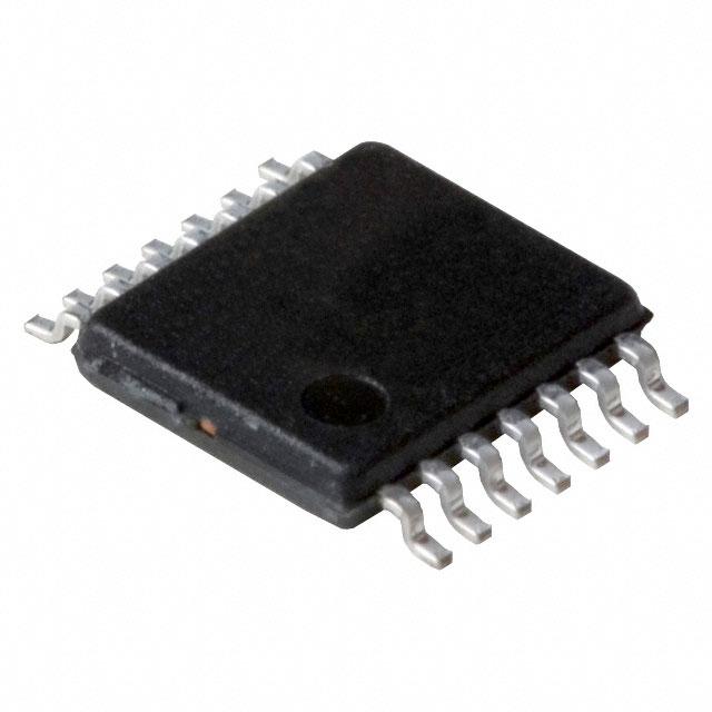


 工商网监
湘ICP备2023018690号
工商网监
湘ICP备2023018690号
