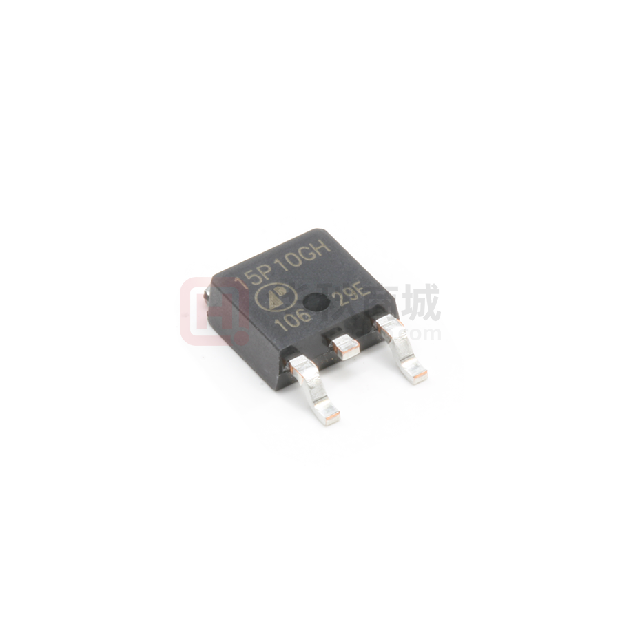
AP15P10GH/J-HF
Halogen-Free Product
Advanced Power
Electronics Corp.
P-CHANNEL ENHANCEMENT MODE
POWER MOSFET
▼ Low Gate Charge
D
▼ Simple Drive Requirement
▼ Fast Switching Characteristic
▼ RoHS Compliant & Halogen-Free
BVDSS
-100V
RDS(ON)
230mΩ
ID
G
-15A
S
Description
AP15P10 series are from Advanced Power innovated design and silicon
process technology to achieve the lowest possible on-resistance and
fast switching performance. It provides the designer with an extreme
efficient device for use in a wide range of power applications.
The TO-252 package is widely preferred for all commercial-industrial
surface mount applications using infrared reflow technique and suited
for high current application due to the low connection resistance. The
through-hole version (AP15P10GJ) are available for low-profile
applications.
G
G
D
D S
S
TO-252(H)
TO-251(J)
Absolute Maximum Ratings@Tj=25oC(unless otherwise specified)
Symbol
Parameter
Rating
Units
VDS
Drain-Source Voltage
-100
V
VGS
Gate-Source Voltage
+20
V
ID@TC=25℃
Drain Current, VGS @ 10V
-15
A
ID@TC=100℃
Drain Current, VGS @ 10V
-9.4
A
-60
A
96
W
1
IDM
Pulsed Drain Current
PD@TC=25℃
Total Power Dissipation
TSTG
Storage Temperature Range
-55 to 150
℃
TJ
Operating Junction Temperature Range
-55 to 150
℃
Thermal Data
Symbol
Parameter
Value
Units
Rthj-c
Maximum Thermal Resistance, Junction-case
1.3
℃/W
Rthj-a
Maximum Thermal Resistance, Junction-ambient (PCB mount) 3
62.5
℃/W
Rthj-a
Maximum Thermal Resistance, Junction-ambient
110
℃/W
Data and specifications subject to change without notice
1
201501125
�AP15P10GH/J-HF
o
Electrical Characteristics@Tj=25 C(unless otherwise specified)
Symbol
BVDSS
Parameter
Test Conditions
Drain-Source Breakdown Voltage
2
Min.
Typ.
Max. Units
VGS=0V, ID=-1mA
-100
-
-
V
VGS=-10V, ID=-6A
-
-
230
mΩ
RDS(ON)
Static Drain-Source On-Resistance
VGS(th)
Gate Threshold Voltage
VDS=VGS, ID=-250uA
-1
-
-3
V
gfs
Forward Transconductance
VDS=-10V, ID=-9A
-
8
-
S
IDSS
Drain-Source Leakage Current
VDS=-100V, VGS=0V
-
-
-25
uA
Drain-Source Leakage Current (T j=125 C) VDS=-80V, VGS=0V
-
-
-250
uA
Gate-Source Leakage
VGS= +20V, VDS=0V
-
-
+100
nA
ID=-9A
-
37
60
nC
o
IGSS
2
Qg
Total Gate Charge
Qgs
Gate-Source Charge
VDS=-80V
-
5
-
nC
Qgd
Gate-Drain ("Miller") Charge
VGS=-10V
-
15
-
nC
2
td(on)
Turn-on Delay Time
VDS=-50V
-
11
-
ns
tr
Rise Time
ID=-9A
-
25
-
ns
td(off)
Turn-off Delay Time
RG=10Ω
-
56
-
ns
tf
Fall Time
VGS=-10V
-
36
-
ns
Ciss
Input Capacitance
VGS=0V
-
1180 1900
pF
Coss
Output Capacitance
VDS=-25V
-
250
-
pF
Crss
Reverse Transfer Capacitance
f=1.0MHz
-
75
-
pF
Rg
Gate Resistance
f=1.0MHz
-
3.6
5
Ω
Min.
Typ.
IS=-9A, VGS=0V
-
-
-1.3
V
Source-Drain Diode
Symbol
VSD
Parameter
Forward On Voltage
2
2
Test Conditions
Max. Units
trr
Reverse Recovery Time
IS=-9A, VGS=0V,
-
95
-
ns
Qrr
Reverse Recovery Charge
dI/dt=-100A/µs
-
410
-
nC
Notes:
1.Pulse width limited by Max. junction temperature.
2.Pulse test
2
3.Surface mounted on 1 in copper pad of FR4 board
THIS PRODUCT IS SENSITIVE TO ELECTROSTATIC DISCHARGE, PLEASE HANDLE WITH CAUTION.
USE OF THIS PRODUCT AS A CRITICAL COMPONENT IN LIFE SUPPORT OR OTHER SIMILAR SYSTEMS IS NOT AUTHORIZED.
APEC DOES NOT ASSUME ANY LIABILITY ARISING OUT OF THE APPLICATION OR USE OF ANY PRODUCT OR CIRCUIT DESCRIBED
HEREIN; NEITHER DOES IT CONVEY ANY LICENSE UNDER ITS PATENT RIGHTS, NOR THE RIGHTS OF OTHERS.
APEC RESERVES THE RIGHT TO MAKE CHANGES WITHOUT FURTHER NOTICE TO ANY PRODUCTS HEREIN TO IMPROVE
RELIABILITY, FUNCTION OR DESIGN.
2
�AP15P10GH/J-HF
30
30
-10V
-10V
TC=150oC
T C =25 o C
-ID , Drain Current (A)
-ID , Drain Current (A)
-7.0V
20
-5.0V
10
-4.5V
-7.0V
20
-5.0V
10
-4.5V
V G = - 3 .0V
V G = - 3 .0V
0
0
0
5
10
15
20
0
25
-V DS , Drain-to-Source Voltage (V)
Fig 1. Typical Output Characteristics
10
15
20
25
Fig 2. Typical Output Characteristics
2.4
550
I D = -6 A
V G = - 10V
I D = -6 A
T C =25 ℃
1.9
Normalized RDS(ON)
450
RDS(ON) (mΩ )
5
-V DS , Drain-to-Source Voltage (V)
350
1.4
0.9
250
0.4
150
2
4
6
8
-50
10
0
50
100
150
T j , Junction Temperature ( o C)
-V GS , Gate-to-Source Voltage (V)
Fig 3. On-Resistance v.s. Gate Voltage
Fig 4. Normalized On-Resistance
v.s. Junction Temperature
1.5
10
8
T j =25 o C
Normalized VGS(th)
-IS(A)
T j =150 o C
6
4
1.1
0.7
2
0
0.3
0
0.4
0.8
-V SD , Source-to-Drain Voltage (V)
Fig 5. Forward Characteristic of
Reverse Diode
1.2
-50
0
50
100
150
T j , Junction Temperature ( o C)
Fig 6. Gate Threshold Voltage v.s.
Junction Temperature
3
�AP15P10GH/J-HF
f=1.0MHz
10
10000
C iss
1000
I D = -9A
V DS = -80V
6
C (pF)
-VGS , Gate to Source Voltage (V)
8
C oss
4
100
C rss
2
10
0
0
10
20
30
1
40
5
9
13
17
21
25
29
-V DS , Drain-to-Source Voltage (V)
Q G , Total Gate Charge (nC)
Fig 7. Gate Charge Characteristics
Fig 8. Typical Capacitance Characteristics
100
Operation in this area
limited by RDS(ON)
Normalized Thermal Response (Rthjc)
1
100us
10
-ID (A)
1ms
10ms
100ms
DC
1
o
T C =25 C
Single Pulse
Duty factor=0.5
0.2
0.1
0.1
0.05
PDM
t
T
0.02
0.01
Duty factor = t/T
Peak Tj = PDM x Rthjc + T C
Single Pulse
0.01
0.1
1
10
100
1000
0.00001
0.0001
-V DS , Drain-to-Source Voltage (V)
0.001
0.01
0.1
1
t , Pulse Width (s)
Fig 9. Maximum Safe Operating Area
Fig 10. Effective Transient Thermal Impedance
10
VG
V DS =-5V
T j =25 o C
-ID , Drain Current (A)
8
T j =150 o C
QG
-10V
6
QGS
QGD
4
2
Charge
Q
0
0
2
4
6
8
-V GS , Gate-to-Source Voltage (V)
Fig 11. Transfer Characteristics
Fig 12. Gate Charge Waveform
4
�AP15P10GH/J-HF
MARKING INFORMATION
TO-251
15P10GJ
Part Number
meet Rohs requirement
for low voltage MOSFET only
Package Code
YWWSSS
Date Code (YWWSSS)
Y:Last Digit Of The Year
WW:Week
SSS:Sequence
TO-252
15P10GH
Part Number
meet Rohs requirement
for low voltage MOSFET only
Package Code
YWWSSS
Date Code (YWWSSS)
Y:Last Digit Of The Year
WW:Week
SSS:Sequence
5
�ADVANCED POWER ELECTRONICS CORP.
Package Outline : TO-252
Millimeters
SYMBOLS
D
D1
E2
E1
F
B2
e
MAX
A2
2.18
2.30
2.40
A3
0.40
0.50
0.65
B
0.40
0.70
1.00
B1
0.50
0.85
1.20
D
6.00
6.50
6.80
D1
4.80
5.35
5.90
4.00 (ref.)
F
2.00
2.63
3.05
F1
0.50
0.85
1.20
E1
5.00
5.70
6.30
E2
0.50
1.10
1.80
e
F1
B
NOM
E3
E3
B1
MIN
e
2.3 (ref)
C
0.35
0.525
0.70
A1
0.00
-
0.25
B2
-
-
1.25
L
0.90
1.34
1.78
.
A2
C
A1
A3
L
1.All Dimensions Are in Millimeters.
2.Dimension Does Not Include Mold Protrusions.
3. Thermal PAD, Body and Pin contour is for reference, it may has little difference by option.
Draw No. M1-H3EFIMT-G-v10
�TO-252
TO-252 FOOTPRINTΚ
6.8mm
7mm
2mm
4.6mm
3mm
.
0.6mm
1.0mm
ADVANCED POWER ELECTRONICS CORP.ʳʳʳʳʳʳʳʳʳʳʳʳʳʳʳʳʳʳʳʳʳʳʳʳʳʳʳʳʳʳʳʳʳʳʳʳʳʳʳʳʳʳʳʳʳʳʳʳʳʳʳʳʳʳʳʳʳʳʳʳʳʳʳʳʳʳʳʳʳʳʳʳʳʳʳDraw No.
M1-H3EFIMT-G-v10
1
�
很抱歉,暂时无法提供与“AP15P10GH-HF”相匹配的价格&库存,您可以联系我们找货
免费人工找货- 国内价格
- 1+3.09318
- 10+2.84373
- 30+2.79384
- 100+2.64417