AP3N1R8MT
Halogen-Free Product
Advanced Power
Electronics Corp.
N-CHANNEL ENHANCEMENT MODE
POWER MOSFET
▼ 100% Rg & UIS Test
D
▼ Simple Drive Requirement
▼ Ultra Low On-resistance
30V
RDS(ON)
1.89mΩ
ID
G
▼ RoHS Compliant & Halogen-Free
BVDSS
4
165A
S
D
Description
AP3N1R8 series are from Advanced Power innovated design and
silicon process technology to achieve the lowest possible onresistance and fast switching performance. It provides the designer
with an extreme efficient device for use in a wide range of power
applications.
The PMPAK ® 5x6 package is special for DC-DC converters
application and the foot print is compatible with SO-8 with backside
heat sink and lower profile.
D
D
D
S
S
S
G
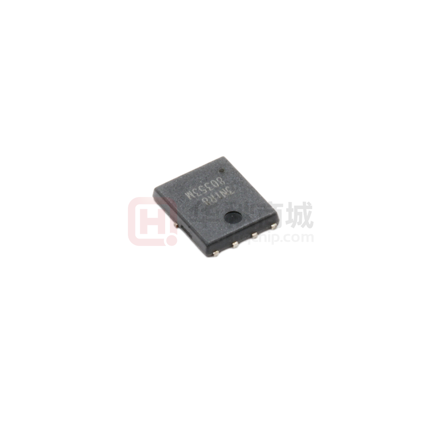
PMPAK® 5x6
Absolute Maximum Ratings@Tj=25oC(unless otherwise specified)
Symbol
VDS
Drain-Source Voltage
VGS
Gate-Source Voltage
ID@TC=25℃
ID@TA=25℃
ID@TA=70℃
.
Parameter
Drain Current (Chip), VGS @ 10V
Drain Current, VGS @ 10V
3
Drain Current, VGS @ 10V
3
4
1
IDM
Pulsed Drain Current
PD@TC=25℃
Total Power Dissipation
PD@TA=25℃
Total Power Dissipation
5
Rating
Units
30
V
+20
V
165
A
40.6
A
32.5
A
300
A
83.3
W
5
W
28.8
mJ
EAS
Single Pulse Avalanche Energy
TSTG
Storage Temperature Range
-55 to 150
℃
TJ
Operating Junction Temperature Range
-55 to 150
℃
Thermal Data
Symbol
Parameter
Rthj-c
Maximum Thermal Resistance, Junction-case
Rthj-a
Maximum Thermal Resistance, Junction-ambient
Data & specifications subject to change without notice
3
Value
Units
1.5
℃/W
25
℃/W
1
201603311
�AP3N1R8MT
Electrical Characteristics@Tj=25oC(unless otherwise specified)
Symbol
BVDSS
RDS(ON)
Parameter
Test Conditions
Drain-Source Breakdown Voltage
Static Drain-Source On-Resistance
2
Min.
Typ.
Max. Units
VGS=0V, ID=250uA
30
-
-
V
VGS=10V, ID=20A
-
-
1.89
mΩ
VGS=4.5V, ID=20A
-
-
3.6
mΩ
VGS(th)
Gate Threshold Voltage
VDS=VGS, ID=250uA
1
-
3
V
gfs
Forward Transconductance
VDS=10V, ID=20A
-
120
-
S
IDSS
Drain-Source Leakage Current
VDS=24V, VGS=0V
-
-
10
uA
IGSS
Gate-Source Leakage
VGS=+20V, VDS=0V
-
-
+100
nA
Qg
Total Gate Charge
ID=20A
-
38
60
nC
Qgs
Gate-Source Charge
VDS=15V
-
7
-
nC
Qgd
Gate-Drain ("Miller") Charge
VGS=4.5V
-
22
-
nC
td(on)
Turn-on Delay Time
VDS=15V
-
14
-
ns
tr
Rise Time
ID=1A
-
12
-
ns
td(off)
Turn-off Delay Time
RG=3.3Ω
-
52
-
ns
tf
Fall Time
VGS=10V
-
42
-
ns
Ciss
Input Capacitance
VGS=0V
-
3030 4850
pF
Coss
Output Capacitance
VDS=25V
Crss
Rg
-
820
-
pF
Reverse Transfer Capacitance
.
f=1.0MHz
-
420
-
pF
Gate Resistance
f=1.0MHz
-
1.3
2.6
Ω
Min.
Typ.
IS=20A, VGS=0V
-
-
1.2
V
Source-Drain Diode
Symbol
Parameter
2
Test Conditions
Max. Units
VSD
Forward On Voltage
trr
Reverse Recovery Time
IS=10A, VGS=0V,
-
47
-
ns
Qrr
Reverse Recovery Charge
dI/dt=100A/µs
-
57
-
nC
Notes:
1.Pulse width limited by Max. junction temperature
2.Pulse test
2
o
3.Surface mounted on 1 in copper pad of FR4 board, t
很抱歉,暂时无法提供与“AP3N1R8MT”相匹配的价格&库存,您可以联系我们找货
免费人工找货- 国内价格
- 1+2.04153
- 10+1.88078
- 30+1.84863
- 100+1.75218
- 国内价格
- 1+2.78410
- 10+2.57000
- 30+2.35580
- 100+2.14160
- 国内价格
- 1+3.31560
- 10+2.61360
- 30+2.31120
- 100+1.93320
- 500+1.76040
- 1000+1.66320