物料型号:AP83T03GH/J-HF
器件简介:
- 该系列是Advanced Power Electronics Corp.创新设计和硅工艺技术的成果,旨在实现尽可能低的导通电阻和快速开关性能。
- 提供了一种在广泛的功率应用中使用的极其高效的设备。
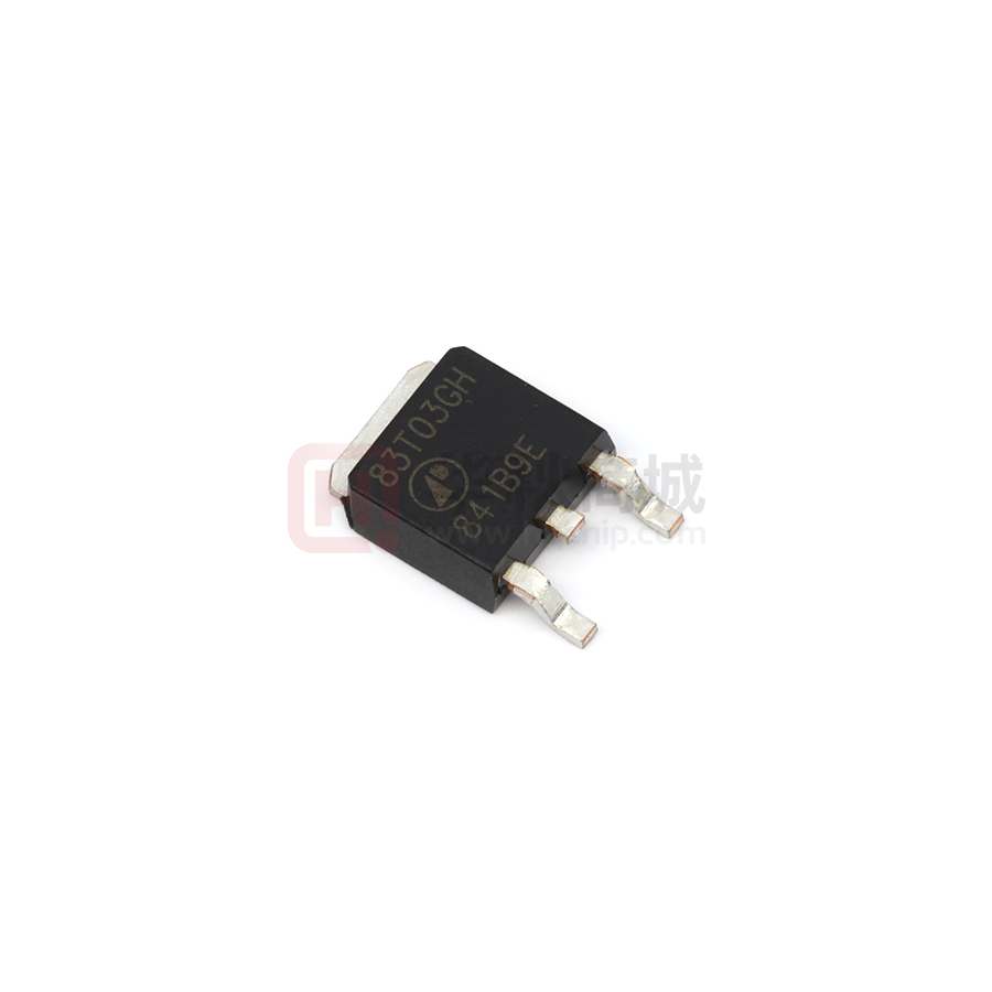
- TO-252封装广泛用于所有商业工业表面贴装应用,使用红外回流技术,并且由于低连接电阻,适合高电流应用。
- 通孔版本(AP83T03GJ)适用于低轮廓应用。
引脚分配:
- 该文档没有明确提供引脚分配的详细信息,但通常TO-252和TO-251封装的MOSFET会有特定的引脚布局。
参数特性:
- 漏源电压(BVpss):30V
- 静态漏源导通电阻(RDS(ON)):最小值为6mΩ
- 漏极电流(ID):在25°C时为75A,100°C时为53A
- 脉冲漏极电流(DM):240A
- 总功耗(Po):60W
- 存储温度范围(TSTG):-55至175°C
- 工作结温范围:-55至175°C
功能详解:
- 该MOSFET具有低导通电阻、简单的驱动要求、快速开关特性,并且符合RoHS和无卤素标准。
- 提供了典型的输出特性图、导通电阻与栅极电压的关系图、结温与导通电阻的关系图、反向二极管的正向特性图、栅极阈值电压与结温的关系图、栅极电荷特性图、典型电容特性图、最大安全工作区域图、有效瞬态热阻抗图、开关时间波形图和栅极电荷波形图。
应用信息:
- 该文档没有明确提供应用信息,但根据其特性,这种MOSFET适用于需要高效率和快速开关的功率应用。
封装信息:
- 提供了TO-252和TO-251两种封装类型。
- TO-252封装适合高电流应用,而TO-251封装适用于低轮廓应用。
注意事项:
- 该产品对静电放电敏感,处理时需谨慎。
- 不允许将该产品作为生命支持或其他类似系统中的关键组件。
- APEC不承担因应用或使用此处描述的任何产品或电路引起的任何责任。
- APEC保留在不另行通知的情况下对此处的任何产品进行更改的权利,以提高可靠性、功能或设计。
标记信息:
- 提供了TO-251和TO-252封装的零件编号、封装代码和日期代码的标记信息。