AP95T07GP-HF
Halogen-Free Product
Advanced Power
Electronics Corp.
N-CHANNEL ENHANCEMENT MODE
POWER MOSFET
▼ Simple Drive Requirement
D
▼ Lower On-resistance
▼ Fast Switching Characteristic
▼ RoHS Compliant & Halogen-Free
BVDSS
75V
RDS(ON)
5mΩ
ID
G
80A
S
Description
AP95T07 series are from Advanced Power innovated design
and silicon process technology to achieve the lowest possible
on-resistance and fast switching performance. It provides the
designer with an extreme efficient device for use in a wide
range of power applications.
The TO-220 package is widely preferred for all commercialindustrial through hole applications. The low thermal resistance
and low package cost contribute to the worldwide popular
package.
G
D
TO-220(P)
S
Absolute Maximum Ratings@Tj=25oC(unless otherwise specified)
Symbol
.
Parameter
VDS
Drain-Source Voltage
VGS
Gate-Source Voltage
3
Rating
Units
75
V
+20
V
ID@TC=25℃
Continuous Drain Current, VGS @ 10V
80
A
ID@TC=100℃
Continuous Drain Current, VGS @ 10V
70
A
320
A
300
W
2
W/℃
450
mJ
1
IDM
Pulsed Drain Current
PD@TC=25℃
Total Power Dissipation
Linear Derating Factor
4
EAS
Single Pulse Avalanche Energy
TSTG
Storage Temperature Range
-55 to 175
℃
TJ
Operating Junction Temperature Range
-55 to 175
℃
Thermal Data
Symbol
Parameter
Rthj-c
Maximum Thermal Resistance, Junction-case
Rthj-a
Maixmum Thermal Resistance, Junction-ambient
Data and specifications subject to change without notice
Value
Units
0.5
℃/W
62
℃/W
1
201408253
�AP95T07GP-HF
Electrical Characteristics@Tj=25oC(unless otherwise specified)
Symbol
BVDSS
Parameter
Test Conditions
Drain-Source Breakdown Voltage
2
Min.
Typ.
Max. Units
VGS=0V, ID=1mA
75
-
-
V
VGS=10V, ID=60A
-
-
5
mΩ
RDS(ON)
Static Drain-Source On-Resistance
VGS(th)
Gate Threshold Voltage
VDS=VGS, ID=250uA
2
-
4
V
gfs
Forward Transconductance
VDS=10V, ID=60A
-
88
-
S
IDSS
Drain-Source Leakage Current
VDS=60V, VGS=0V
-
-
25
uA
IGSS
Gate-Source Leakage
VGS= +20V, VDS=0V
-
-
+100
nA
ID=80A
-
85
135
nC
2
Qg
Total Gate Charge
Qgs
Gate-Source Charge
VDS=40V
-
25
-
nC
Qgd
Gate-Drain ("Miller") Charge
VGS=10V
-
36
-
nC
VDS=40V
-
22
-
ns
2
td(on)
Turn-on Delay Time
tr
Rise Time
ID=80A
-
160
-
ns
td(off)
Turn-off Delay Time
RG=3.3Ω
-
38
-
ns
tf
Fall Time
VGS=10V
-
165
-
ns
Ciss
Input Capacitance
VGS=0V
-
4290 6870
pF
Coss
Output Capacitance
VDS=25V
-
985
-
pF
Crss
Reverse Transfer Capacitance
f=1.0MHz
-
390
-
pF
Rg
Gate Resistance
f=1.0MHz
-
1.2
2.4
Ω
Min.
Typ.
IS=60A, VGS=0V
-
-
1.3
V
IS=40A, VGS=0V
-
75
-
ns
dI/dt=100A/µs
-
190
-
nC
.
Source-Drain Diode
Symbol
VSD
Parameter
2
Forward On Voltage
2
trr
Reverse Recovery Time
Qrr
Reverse Recovery Charge
Test Conditions
Max. Units
Notes:
1.Pulse width limited by Max. junction temperature.
2.Pulse test
3.Package limitation current is 80A, calculated continuous current
based on maximum allowable junction temperature is 169A.
4.Starting Tj=25oC , L=1mH , IAS=30A.
THIS PRODUCT IS SENSITIVE TO ELECTROSTATIC DISCHARGE, PLEASE HANDLE WITH CAUTION.
USE OF THIS PRODUCT AS A CRITICAL COMPONENT IN LIFE SUPPORT OR OTHER SIMILAR SYSTEMS IS NOT AUTHORIZED.
APEC DOES NOT ASSUME ANY LIABILITY ARISING OUT OF THE APPLICATION OR USE OF ANY PRODUCT OR CIRCUIT DESCRIBED
HEREIN; NEITHER DOES IT CONVEY ANY LICENSE UNDER ITS PATENT RIGHTS, NOR THE RIGHTS OF OTHERS.
APEC RESERVES THE RIGHT TO MAKE CHANGES WITHOUT FURTHER NOTICE TO ANY PRODUCTS HEREIN TO IMPROVE
RELIABILITY, FUNCTION OR DESIGN.
2
�AP95T07GP-HF
250
120
10 V
9.0 V
8.0 V
7.0 V
ID , Drain Current (A)
200
10V
9.0V
8.0V
7.0V
V G = 6.0 V
T C = 1 75 o C
100
ID , Drain Current (A)
o
T C = 25 C
150
100
V G = 6.0 V
80
60
40
50
20
0
0
0
1
2
3
0
4
Fig 1. Typical Output Characteristics
2
3
Fig 2. Typical Output Characteristics
12
2.4
I D =30A
I D =60A
V G =10V
T C =25 o C
8
.
Normalized RDS(ON)
2.0
10
RDS(ON) (mΩ)
1
V DS , Drain-to-Source Voltage (V)
V DS , Drain-to-Source Voltage (V)
1.6
1.2
6
0.8
4
0.4
4
5
6
7
8
9
10
-50
0
50
100
150
200
T j , Junction Temperature ( o C)
V GS Gate-to-Source Voltage (V)
Fig 3. On-Resistance v.s. Gate Voltage
Fig 4. Normalized On-Resistance
v.s. Junction Temperature
1.4
60
50
1.2
o
T j =25 C
Normalized VGS(th)
T j =175 C
40
IS(A)
o
30
20
1
0.8
0.6
10
0.4
0
0
0.2
0.4
0.6
0.8
1
1.2
V SD , Source-to-Drain Voltage (V)
Fig 5. Forward Characteristic of
Reverse Diode
1.4
-50
0
50
100
150
200
T j ,Junction Temperature ( o C)
Fig 6. Gate Threshold Voltage v.s.
Junction Temperature
3
�AP95T07GP-HF
f=1.0MHz
14
10000
C iss
V DS = 40 V
V DS = 48 V
V DS = 64 V
10
C (pF)
VGS , Gate to Source Voltage (V)
I D = 80 A
12
8
1000
C oss
6
C rss
4
2
0
100
0
20
40
60
80
100
120
1
5
9
Q G , Total Gate Charge (nC)
13
17
21
25
29
V DS ,Drain-to-Source Voltage (V)
Fig 7. Gate Charge Characteristics
Fig 8. Typical Capacitance Characteristics
1000
100us
ID (A)
100
1ms
.
10ms
10
100ms
DC
o
T c =25 C
Single Pulse
Normalized Thermal Response (Rthjc)
1
Duty factor=0.5
0.2
0.1
0.1
0.05
PDM
t
0.02
T
0.01
Duty factor = t/T
Peak Tj = PDM x Rthjc + T C
Single Pulse
0.01
1
0.1
1
10
100
1000
0.00001
0.0001
V DS , Drain-to-Source Voltage (V)
Fig 9. Maximum Safe Operating Area
0.001
0.01
0.1
1
t , Pulse Width (s)
Fig 10. Effective Transient Thermal Impedance
VG
VDS
90%
QG
10V
QGS
QGD
10%
VGS
td(on) tr
td(off) tf
Fig 11. Switching Time Waveform
Charge
Q
Fig 12. Gate Charge Waveform
4
�AP95T07GP-HF
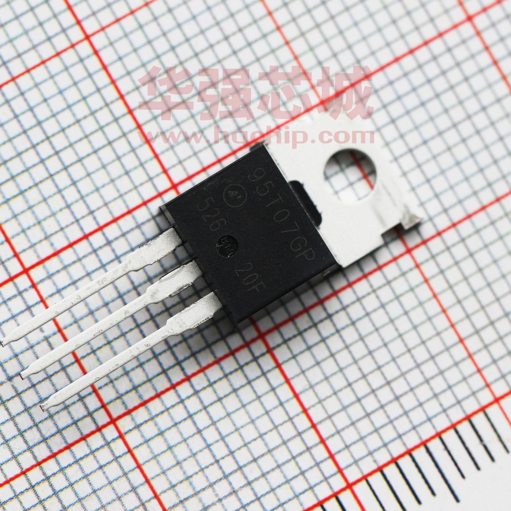
MARKING INFORMATION
95T07GP
Part Number
meet Rohs requirement
for low voltage MOSFET only
Package Code
YWWSSS
Date Code (YWWSSS)
Y:Last Digit Of The Year
WW:Week
SSS:Sequence
.
5
�
很抱歉,暂时无法提供与“AP95T07GP-HF”相匹配的价格&库存,您可以联系我们找货
免费人工找货