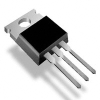
IRF830
RoHS-compliant Product
Advanced Power Electronics Corp.
▼ Ease of Paralleling ▼ Fast Switching Characteristic ▼ Simple Drive Requirement G
N-CHANNEL ENHANCEMENT MODE POWER MOSFET D
BVDSS RDS(ON) ID
500V 1.5Ω 4.5A
S
Description
APEC MOSFET provide the power designer with the best combination of fast switching , lower on-resistance and reasonable cost. The TO-220 and package is universally preferred for all commercial-industrial applications. The device is suited for switch mode power supplies ,DC-AC converters and high current high speed switching circuits.
G
D
S
TO-220(P)
Absolute Maximum Ratings
Symbol VDS VGS ID@TC=25℃ ID@TC=100℃ IDM PD@TC=25℃ EAS IAR TSTG TJ Parameter Drain-Source Voltage Gate-Source Voltage Continuous Drain Current, V GS @ 10V Continuous Drain Current, V GS @ 10V Pulsed Drain Current
1
Rating 500 ±20 4.5 2.8 18 74 0.59
2
Units V V A A A W W/ ℃ mJ A ℃ ℃
Total Power Dissipation Linear Derating Factor Single Pulse Avalanche Energy Avalanche Current Storage Temperature Range Operating Junction Temperature Range
101 4.5 -55 to 150 -55 to 150
Thermal Data
Symbol Rthj-c Rthj-a Parameter Thermal Resistance Junction-case Thermal Resistance Junction-ambient Max. Max. Value 1.7 62 Unit ℃/W ℃/W
200420071-1/4
Data & specifications subject to change without notice
�IRF830
Electrical Characteristics@Tj=25 C(unless otherwise specified)
Symbol BVDSS RDS(ON) VGS(th) gfs IDSS IGSS Qg Qgs Qgd td(on) tr td(off) tf Ciss Coss Crss Rg Parameter Drain-Source Breakdown Voltage Static Drain-Source On-Resistance Gate Threshold Voltage Forward Transconductance
Drain-Source Leakage Current (Tj=25 C) Drain-Source Leakage Current (Tj=125 C)
o o
o
Test Conditions VGS=0V, ID=1mA VGS=10V, ID=2.7A VDS=VGS, ID=250uA VDS=10V, ID=2.7A VDS=500V, VGS=0V VDS=400V, VGS=0V VGS=±20V ID=3.1A VDS=400V VGS=10V VDD=250V ID=3.1A RG=12Ω,VGS=10V RD=80.6Ω VGS=0V VDS=25V f=1.0MHz f=1.0MHz
Min. 500 2 -
Typ. 2.4 28 4 16 10 15 41 20 710 170 60 2
Max. Units 1.5 4 25 250 ±100 45 1140 3.0 V Ω V S uA uA nA nC nC nC ns ns ns ns pF pF pF Ω
Gate-Source Leakage Total Gate Charge
3
Gate-Source Charge Gate-Drain ("Miller") Charge Turn-on Delay Time Rise Time Turn-off Delay Time Fall Time Input Capacitance Output Capacitance Reverse Transfer Capacitance Gate Resistance
3
Source-Drain Diode
Symbol VSD Parameter Forward On Voltage
3 3
Test Conditions Tj=25℃, IS=4.5A, VGS=0V IS=3.1A, VGS=0V, dI/dt=100A/µs
Min. -
Typ. 370 3.9
Max. Units 1.5 V ns uC
trr
Qrr Notes:
Reverse Recovery Time
Reverse Recovery Charge
1.Pulse width limited by Max. junction temperature.
o 2.Starting Tj=25 C , VDD=50V , L=10mH , RG=25Ω
3.Pulse test
THIS PRODUCT IS ELECTROSTATIC SENSITIVE, PLEASE HANDLE WITH CAUTION. THIS PRODUCT HAS BEEN QUALIFIED FOR USE IN CONSUMER APPLICATIONS. APPLICATIONS OR USE IN LIFE SUPPORT OR OTHER SIMILAR MISSION-CRITICAL DEVICES OR SYSTEMS ARE NOT AUTHORIZED. 2/4
�IRF830
8
5
T C =25 C
o
ID , Drain Current (A)
ID , Drain Current (A)
6
10V 7.0V 6.0V
T C =150 o C
4
10V 7 .0V 6 .0V
3
5 .0 V
4
2
V G = 4. 5 V
1
2
5.0V V G =4.5V
0 0 4 8 12 16 20
0
0
4
8
12
16
20
24
V DS , Drain-to-Source Voltage (V)
V DS , Drain-to-Source Voltage (V)
Fig 1. Typical Output Characteristics
Fig 2. Typical Output Characteristics
1.2
3
I D =2.7A V G =10V Normalized BVDSS (V)
1.1
Normalized RDS(ON)
2
1
1
0.9
0.8 -50 0 50 100 150
0 -50 0 50 100 150
T j , Junction Temperature ( C)
o
T j , Junction Temperature ( o C )
Fig 3. Normalized BVDSS v.s. Junction Temperature
10 1.4
Fig 4. Normalized On-Resistance v.s. Junction Temperature
8
1.2
T j = 150 o C
6
T j = 25 o C
Normalized VGS(th) (V)
1
IS (A)
4
0.8
2
0.6
0 0 0.2 0.4 0.6 0.8 1 1.2 1.4
0.4 -50 0 50 100 150
V SD , Source-to-Drain Voltage (V)
T j , Junction Temperature ( C)
o
Fig 5. Forward Characteristic of
Reverse Diode
Fig 6. Gate Threshold Voltage v.s. Junction Temperature
3/4
�IRF830
f=1.0MHz
12 10000
I D =3.1A
10
VGS , Gate to Source Voltage (V)
8
V DS =100V V DS =250V V DS =400V C (pF)
1000
C iss
6
C oss
4 100
C rss
2
0 0 10 20 30 40
10
1 5 9 13 17 21 25 29
Q G , Total Gate Charge (nC)
V DS , Drain-to-Source Voltage (V)
Fig 7. Gate Charge Characteristics
Fig 8. Typical Capacitance Characteristics
100
1
Normalized Thermal Response (Rthjc)
Duty factor=0.5
10
0.2
ID (A)
100us 1ms
1
0.1
0.1
0.05
PDM
t
0.02 0.01
T c =25 C Single Pulse
o
10ms 100m 1s DC
T
Duty factor = t/T Peak Tj = PDM x Rthjc + T C
Single Pulse
0.1 1 10 100
0.01 0.00001 0.0001 0.001 0.01 0.1 1
1000
V DS , Drain-to-Source Voltage (V)
t , Pulse Width (s)
Fig 9. Maximum Safe Operating Area
Fig 10. Effective Transient Thermal Impedance
VDS 90%
VG QG 10V QGS QGD
10% VGS td(on) tr td(off) tf Charge Q
Fig 11. Switching Time Waveform
Fig 12. Gate Charge Waveform
4/4
�
很抱歉,暂时无法提供与“IRF830”相匹配的价格&库存,您可以联系我们找货
免费人工找货