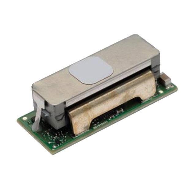
IND080 Hornet: Non-Isolated DC-DC Voltage Regulator Modules
12Vdc input; 0.8Vdc to 2Vdc output; 80W Max Power
Vin+
VIN
PGOOD
Vout+
VOUT
VS+
MODULE
Applications
✓
✓
✓
TRIM
Cin
SEQ
Industrial Equipment
Control Boards
Test Equipment
SHARE
ON/OFF
GND
Features
•Electrical
12V Input
voltage with ±20% Tolerance
• Output voltage programmable from 0.8Vdc to 2Vdc via
external resistor
• Remote On/Off for optional external control
• Power Good signal for external monitoring
• Fixed switching frequency
• Output overcurrent protection (non-latching)
• Share and Sequence available for advanced loads
Co
RTrim
SIG_GND
SYNC GND VS-
Mechanical Features
•
•
•
•
Small size: 33.02 mm x 13.46 mm x 10.9 mm (1.3
in x 0.53 in x 0.429 in)
Operating range: -40°C to 105°C ambient
Operating shock to 40G per Mil Std. 810G,
Method 516.4 Procedure I
Operating vibration per Mil Std. 810G, Method
514.5 Procedure I
Process and Safety
•
•
Qualified for 1000h High Temperature Operating Bias, 1000h 85RH/85°C Temperature, Humidity and Bias, 700 cycle -40 to
125°C thermal cycling
ANSI/UL* 62368-1 and CAN/CSA† C22.2 No. 62368-1 Recognized, DIN VDE‡ 0868-1/A11:2017 (EN62368-1:2014/A11:2017)
ISO** 9001 and ISO 14001 certified manufacturing facilities
Compliant to RoHS Directive 2011/65/EU and amended Directive (EU) 2015/863
Compliant to REACH Directive (EC) No 1907/2006
Compatible in a Pb-free or SnPb reflow environment.
Suitable for aqueous clean.
Suitable for conformal coating with dip and vapor deposition. Conformal coating can provide the protection to meet Salt
Fog Test per IEC 60068-2-52 (Severity 3) and Mixed Gas Flow test per Telcordia GR-3108 Outdoor Levels.
3 year warranty
•
•
•
•
•
•
•
•
Device Code
Input Voltage
Output
Voltage
Output
Current (Max.)
On/Off Logic
Comcode
IND080
9.6 – 14.4Vdc
0.6 – 2.0Vdc
40A
Negative
1600102901A
Thermal Performance
Full rated output with natural convection up to 63°C at 1.2Vout and up to 60°C at 1.8Vout. Thermal curves for 1.2V, and 1.8Vout below.
45
45
40
40
35
35
30
0.5m/s
(100LFM)
30
1m/s
(200LFM)
25
20
NC
NC
1.2Vout
1m/s
(200LFM)
1.5m/s
20
1.5m/s
(300LFM)
2m/s
(400LFM)
15
Current (A) vs. Temp ( C)
2m/s
(400LFM)
15
0.5m/s
(100LFM)
25
10
1.8 Vout
Current (A) vs. Temp ( C)
5
10
45
55
May 13, 2021
65
75
85
95
105
45
55
65
75
85
95
©2017 General Electric Company. All rights reserved.
105
Page 1
�Electrical Specifications
Parameter
Device
Symbol
Min
Typ
Max
Unit
All
VIN
9.6
12
14.4
Vdc
VO,set =
2Vdc
IIN,No load
Operating Input Voltage
Input No Load Current
(VIN = 12.0Vdc, IO = 0, module enabled)
External Capacitance, Ceramic ESR ≥ 1 mΩ
All
CO, max
Efficiency 12VINDC, TA=25°C, I=12A, Vo=1.2 to 5Vdc
η
104
mA
6x47
6x47*
⎯
82.8(1.2V), 88.2(1.8V), 91.6(3.3V),
93.9(5V)
600
⎯
⎯
μF
%
Switching Frequency
All
fsw
kHz
Output Voltage (Over all line, load, and temperature conditions)
All
VO, set
-3.0
⎯
+3.0
% VO, set
On/Off Logic High (MODULE OFF) Input High Voltage
All
VIH
2
⎯
14.4
Vdc
On/ Off Logic Low (MODULE ON) Input Low Voltage
All
VIL
-0.2
―
0.4
Vdc
PGOOD (Power Good)
Signal Interface Open Drain, Vsupply 5VDC
Overvoltage threshold for PGOOD ON
All
103
108
113
%VO, set
Overvoltage threshold for PGOOD OFF
All
105
110
115
%VO, set
Undervoltage threshold for PGOOD ON
All
87
92
97
%VO, set
Undervoltage threshold for PGOOD OFF
All
85
90
95
%VO, set
Pulldown resistance of PGOOD pin
All
50
Sink current capability into PGOOD pin
All
5
mA
480
kHz
Frequency Synchronization (SYNC)
Synchronization Frequency Range
All
All
350
High-Level Input Voltage
All
VIH
Low-Level Input Voltage
Input Current, SYNC
Minimum Pulse Width, SYNC
All
All
All
VIL
ISYNC
tSYNC
2.0
V
100
V
nA
ns
Maximum SYNC rise time
All
tSYNC_SH
100
ns
0.4
100
*Additional External Capacitance possible using Tunable Loop
Characteristic Curves
The following figures provide typical characteristics for the IND080 Hornet at 25oC.
40
6x47uF Ext Cap
Ripple (m Vp-p)
8x47uF Ext Cap
30
10x47uF Ext Cap
20
10
0
0.8
1
1.2
1.4
1.6
1.8
2
Output Voltage(Volts)
Figure 1. Output Ripple Voltage(20MHz BW) for various output
voltages and external caps @12Vin. Additional Decoupling cap of
0.1uF used on input and output side
Figure 2. Typical Start-up using Input Voltage (Vin=12V,
Vout = Vout, max, Iout = Iout, max)
Trim
Without an external resistor between Trim and GND pins, the output of the module will be 0.6Vdc. Rtrim for a desired output
voltage, should be as per the following table. The formula in the last column helps determine Rtrim for other voltages.
Vo (V)
0.9
1.2
1.5
1.8
Rtrim (kΩ)
40
20
13.3
10
May 13, 2021
12
Rtrim =
k
(Vo − 0.6)
©2017 General Electric Company. All rights reserved.
Page 2
�Safety Considerations
For safety agency approval, the power module must be installed in compliance with the spacing and separation requirements of
the end-use safety agency standards listed on the first page of this document. For the converter output to be considered meeting
the requirements of safety extra-low voltage (SELV) or ES1, the input must meet SELV/ES1 requirements. The power module has
extra-low voltage (ELV) outputs when all inputs are ELV. The input to these units is to be provided with a fast-acting fuse with a
maximum rating of 30A, 100V (for example, Littlefuse 456 series) in the positive input lead.
Tunable Loop
The module is designed for 1x47uF capacitor on its output. For applications where more than 1x47uF capacitors would be used
on the output, an additional Resistor (Rtune) and Capacitor (Ctune) would be required in the circuit schematic to compensate for
the additional capacitance. The placement is between the Sense+ pin and Trim pin as per figure below:
The recommended values for Rtune and Ctune for
different amounts of external capacitance are as per the
table below:
VOUT
VS+
RTune
MODULE
CO
Co
RTUNE
CTune
T RIM
CTUNE
RTr im
6x47F 8x47F
10x47F 12x47F 20x47F
330Ω
330Ω
330Ω
330Ω
200Ω
330pF
820pF
1200pF
1500pF
3300pF
SIG_GND
GND
Figure 3. Circuit diagram showing connection of RTUNE and
CTUNE to tune the control loop of the module
PowerGood (PG)
This is an open-drain output to indicate that the output voltage is within the regulation limits of the module. The PGOOD signal
will be de-asserted to a low state if any condition such as overtemperature, overcurrent or loss of regulation occurs that would
result in the output voltage going ±10% outside the setpoint value. The default value of PGOOD ON thresholds are set at ±8% of
the nominal Vset value, and PGOOD OFF thresholds are set at ±10% of the nominal Vset. For example, if the nominal voltage
(Vset) is set at 1.0V, then the PGOOD ON thresholds will be active anytime the output voltage is between 0.92V and 1.08V, and
PGOOD OFF thresholds are active at 0.90V and 1.10V respectively. If not used, leave unconnected.
Synchronization (SYNC)
MODULE
SYNC
+
─
GND
Figure 4. External source connections to synchronize
switching frequency of the module.
May 13, 2021
The module switching frequency can be synchronized to a
signal with an external frequency within a specified range.
Synchronization can be done by using the external signal
applied to the SYNC pin of the module as shown in Fig. 4,
with the converter being synchronized by the rising edge
of the external signal. The Electrical Specifications table
specifies the requirements of the external SYNC signal. If
the SYNC pin is not used, the module should free run at the
default switching frequency. If synchronization is not being
used, connect the SYNC pin to GND.
©2017 General Electric Company. All rights reserved.
Page 3
�Recommended Pad Layout
Dimensions are in millimeters and (inches).
Tolerances: x.x mm 0.5 mm (x.xx in. 0.02 in.) [unless otherwise indicated] x.xx mm 0.25 mm (x.xxx in 0.010 in.)
SHARE must be left
open if not being used
May 13, 2021
NC
NC
NC
NC
Leave open if not used
*SYNC must be connected to
SIG_GND if not being used
NC
©2017 General Electric Company. All rights reserved.
Page 4
�be digitally turned ON as that does not ensure that all
modules being paralleled turn on at the same time.
Active Load Sharing (Share Function)
For additional power requirements, the Mega DLynxTM power
module is also equipped with paralleling capability. Up to five
modules can be configured in parallel, with active load
sharing.
To implement paralleling, the following conditions must be
satisfied.
•
All modules connected in parallel must be frequency
synchronized where they are switching at the same
frequency. This is done by using the SYNC function of the
module and connecting to an external frequency source.
Modules can be interleaved to reduce input
ripple/filtering requirements.
•
The share pins of all units in parallel must be connected
together. The path of these connections should be as
direct as possible.
•
The remote sense connections to all modules should be
made that to the same points for the output, i.e. all VS+
and VS- terminals for all modules are connected to the
power bus at the same points.
•
For converters operating in parallel, tunable loop
components “RTUNE” and “CTUNE” must be selected to
meet the required transient specification. For providing
better noise immunity, we recommend that RTUNE value
to be greater than 300Ω.
Some special considerations apply for design of converters in
parallel operation:
•
•
When sizing the number of modules required for parallel
operation, take note of the fact that current sharing has
some tolerance. In addition, under transient conditions
such as a dynamic load change and during startup, all
converter output currents will not be equal. To allow for
such variation and avoid the likelihood of a converter
shutting off due to a current overload, the total capacity
of the paralleled system should be no more than 90% of
the sum of the individual converters. As an example, for
a system of four modules in parallel, the total current
drawn should be less that 90% of (3 x 40A), i.e. less than
108 A.
All modules should be turned ON and OFF together. This
is so that all modules come up at the same time avoiding
the problem of one converter sourcing current into the
other leading to an overcurrent trip condition. To ensure
that all modules come up simultaneously, the on/off pins
of all paralleled converters should be tied together and
the converters enabled and disabled using the on/off pin.
Note that this means that converters in parallel cannot
May 13, 2021
•
If the Sequencing function is being used to start-up and
shut down modules and the module is being held to 0V
by the tracking signal then there may be small deviations
on the module output. This is due to controller duty cycle
limitations encountered in trying to hold the voltage
down near 0V.
•
The share bus is not designed for redundant operation
and the system will be non-functional upon failure of one
of the units when multiple units are in parallel. In
particular, if one of the converters shuts down during
operation, the other converters may also shut down due
to their outputs hitting current limit. In such a situation,
unless a coordinated restart is ensured, the system may
never properly restart since different converters will try
to restart at different times causing an overload
condition and subsequent shutdown. This situation can
be avoided by having an external output voltage monitor
circuit that detects a shutdown condition and forces all
converters to shut down and restart together.
When not using the active load share feature, share pins
should be left unconnected.
Output Voltage Sequencing
The voltage applied to the SEQ pin should be scaled down by the
same ratio as used to scale the output voltage down to the
reference voltage of the module. Minimum recommended delay
between the ON/OFF signal and the sequencing signal is 10ms to
ensure that the module output is ramped up according to the
sequencing signal. Final value of the sequencing voltage must be set
higher than the set-point voltage of the module. The module’s
output can track the SEQ pin signal with slopes of up to 0.5V/msec
during power-up or power-down.
Module
V
SEQ
20K
SEQ
R1=Rtrim
100 pF
SIG_GND
Figure 5. Circuit showing connection of the sequencing signal to
the SEQ pin.
©2017 General Electric Company. All rights reserved.
Page 5
�Nozzle Recommendations
Pb-free Reflow Profile
The minimum recommended inside nozzle diameter for reliable
operation is 3mm. The maximum nozzle outer diameter, which will
safely fit within the allowable component spacing, is 7 mm.
Power Systems will comply with J-STD-020 Rev. D (Moisture/Reflow
Sensitivity Classification for Nonhermetic Solid State Surface Mount
Devices) for both Pb-free solder profiles and MSL classification
procedures. The suggested Pb-free solder paste is Sn/Ag/Cu (SAC).
The following profile is the recommended linear reflow profile using
Sn/Ag/Cu solder . Soldering outside of the recommended profile
requires testing to verify results and performance.
Bottom Side / First Side Assembly
This module is not recommended for assembly on the bottom side
of a customer board. If such an assembly is attempted, components
may fall off the module during the second reflow process
300
Lead Free Soldering
Per J-STD-020 Rev. D
Peak Temp 260°C
MSL Rating
The modules have a MSL rating of 2a.
Reflow Temp (°C)
The modules are lead-free (Pb-free) and RoHS compliant and fully
compatible in a Pb-free soldering process. Failure to observe the
instructions below may result in the failure of or cause damage to
the modules and can adversely affect long-term reliability
250
200
* Min. Time Above 235°C
15 Seconds
Cooling
Zone
150
Heating Zone
1°C/Second
*Time Above 217°C
60 Seconds
100
50
0
Reflow Time (Seconds)
Storage and Handling
J-STD-033 Rev. A (Handling, Packing, Shipping and Use of
Moisture/Reflow Sensitive Surface Mount Devices) is recommended.
Moisture barrier bags (MBB) with desiccant are required for MSL
ratings of 2 or greater. These sealed packages should not be broken
until time of use. Once the original package is broken, the floor life
of the product at conditions of 30°C and 60% relative humidity
varies according to the MSL rating (see J-STD-033A). The shelf life
for dry packed SMT packages will be a minimum of 12 months from
the bag seal date, when stored at the following conditions: < 40° C,
< 90% relative humidity.
Post Solder Cleaning and Drying Considerations
Post solder cleaning is usually the final circuit-board assembly
process prior to electrical board testing. The result of inadequate
cleaning and drying can affect both the reliability of a power module
and the testability of the finished circuit-board assembly
Contact Us
For more information, call us at
USA/Canada:
+1 888 546 3243, or +1 972 244 9288
Asia-Pacific:
+86-21-53899666
Europe, Middle-East and Africa:
+49.89.878067-280
Go.ABB/Industrial
GE Critical Power reserves the right to make changes to the product(s) or information contained herein without notice, and no
liability is assumed as a result of their use or application. No rights under any patent accompany the sale of any such
product(s) or information.
May 13, 2021
©2017 General Electric Company. All International rights reserved.
Version 1.4
�