Data Sheet
June 2001
JAHW050A and JAHW075A Power Modules:
dc-dc Converters; 36 Vdc to 75 Vdc Input, 5 Vdc Output; 50 W to 75 W
Features
■
The JAHW Series Power Modules use advanced, surfacemount technology and deliver high-quality, efficient, and
compact dc-dc conversion.
Applications
■
Distributed power architectures
■
Workstations
■
Computer equipment
■
Communications equipment
■
High power density
■
Very high efficiency: 90% typical
■
Low output noise
■
Constant frequency
■
Industry-standard pinout
■
Metal baseplate
■
2:1 input voltage range
■
Overcurrent protection (hiccup mode)
■
Remote on/off
■
Adjustable output voltage
■
Remote sense
■
Output overvoltage protection (hiccup mode)
■
Overtemperature protection (hiccup mode)
■
Case ground pin
■
ISO* 9001 Certified manufacturing facilities
■
Options
■
Heat sinks available for extended operation
■
Choice of remote on/off logic configuration
■
Latching protection features
■
■
Description
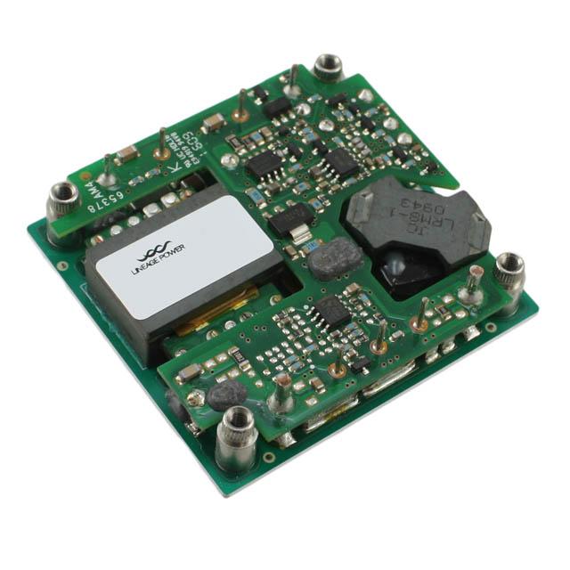
Small size: 61.0 mm x 57.9 mm x 12.7 mm
(2.40 in. x 2.28 in. x 0.50 in.)
Meets the voltage and current requirements for
ETSI 300-132-2 and complies with and is Licensed
for Basic Insulation rating per EN60950 (-B version
only)
UL† 60950 Recognized, CSA‡ 22.2 No. 60950-00
Certified, and VDE § 0805 (IEC60950, IEC950)
Licensed
CE mark meets 73/23/EEC and 93/68/EEC
directives**
The JAHW050A and JAHW075A Power Modules are dc-dc converters that operate over an input voltage range
of 36 Vdc to 75 Vdc and provide a precisely regulated dc output. The outputs are fully isolated from the inputs,
allowing versatile polarity configurations and grounding connections. The modules have maximum power ratings from 50 W to 75 W at a typical full-load efficiency of 90%.
The sealed modules offer a metal baseplate for excellent thermal performance. Threaded-through holes are provided to allow easy mounting or addition of a heat sink for high-temperature applications. The standard feature set
includes remote sensing, output trim, and remote on/off for convenient flexibility in distributed power applications.
* ISO is a registered trademark of the International Organization for Standardization.
† UL is a registered trademark of Underwriters Laboratories, Inc.
‡ CSA is a registered trademark of Canadian Standards Association.
§ VDE is a trademark of Verband Deutscher Elektrotechniker e.V.
** This product is intended for integration into end-use equipment. All the required procedures for CE marking of end-use equipment should be followed. (The CE mark is placed on
selected products.)
�JAHW050A and JAHW075A Power Modules:
dc-dc Converters; 36 Vdc to 75 Vdc Input, 5 Vdc Output; 50 W to 75 W
Data Sheet
June 2001
Absolute Maximum Ratings
Stresses in excess of the absolute maximum ratings can cause permanent damage to the device. These are absolute stress ratings only. Functional operation of the device is not implied at these or any other conditions in excess
of those given in the operations sections of the data sheet. Exposure to absolute maximum ratings for extended
periods can adversely affect device reliability.
Parameter
Symbol
Min
Max
Unit
VI
VI, trans
—
—
80
100
Vdc
V
Operating Case Temperature
(See Thermal Considerations section.)
TC
–40
100
°C
Storage Temperature
Tstg
–55
125
°C
I/O Isolation Voltage (for 1 minute)
—
—
1500
Vdc
Input Voltage:
Continuous
Transient (100 ms)
Electrical Specifications
Unless otherwise indicated, specifications apply over all operating input voltage, resistive load, and temperature
conditions.
Table 1. Input Specifications
Parameter
Symbol
Min
Typ
Max
Unit
VI
36
48
75
Vdc
II, max
II, max
—
—
—
—
1.7
2.6
A
A
Inrush Transient
i2t
—
—
1.0
A2s
Input Reflected-ripple Current, Peak-to-peak
(5 Hz to 20 MHz, 12 µH source impedance;
see Figure 12.)
II
—
5
—
mAp-p
Input Ripple Rejection (120 Hz)
—
—
60
—
dB
Operating Input Voltage
Maximum Input Current
(VI = 0 V to 75 V; IO = IO, max):
JAHW050A (See Figure 1.)
JAHW075A (See Figure 2.)
Fusing Considerations
CAUTION: This power module is not internally fused. An input line fuse must always be used.
This encapsulated power module can be used in a wide variety of applications, ranging from simple stand-alone
operation to an integrated part of a sophisticated power architecture. To preserve maximum flexibility, internal fusing is not included; however, to achieve maximum safety and system protection, always use an input line fuse. The
safety agencies require a normal-blow fuse with a maximum rating of 15 A (see Safety Considerations section).
Based on the information provided in this data sheet on inrush energy and maximum dc input current, the same
type of fuse with a lower rating can be used. Refer to the fuse manufacturer’s data for further information.
2
Tyco Electronics Corp.
�JAHW050A and JAHW075A Power Modules:
dc-dc Converters; 36 Vdc to 75 Vdc Input, 5 Vdc Output; 50 W to 75 W
Data Sheet
June 2001
Electrical Specifications (continued)
Table 2. Output Specifications
Device
Symbol
Min
Typ
Max
Unit
Output Voltage Set Point
(VI = 48 V; IO = IO, max; TC = 25 °C)
Parameter
All
VO, set
4.92
5.0
5.08
Vdc
Output Voltage
(Over all operating input voltage, resistive load,
and temperature conditions until end of life. See
Figure 14.)
All
VO
4.85
—
5.15
Vdc
Output Regulation:
Line (VI = 36 V to 75 V)
Load (IO = IO, min to IO, max)
Temperature (TC = –40 °C to +100 °C)
All
All
All
—
—
—
—
—
—
0.01
0.05
15
0.1
0.2
50
%VO
%VO
mV
Output Ripple and Noise Voltage
(See Figure 13.):
RMS
Peak-to-peak (5 Hz to 20 MHz)
All
All
—
—
—
—
—
—
50
100
mVrms
mVp-p
External Load Capacitance (electrolytic)
All
—
0‡
—
*
µF
Output Current
(At IO < IO, min, the modules may exceed output
ripple specifications.)
JAHW050A
JAHW075A
IO
IO
0.5
0.5
—
—
10
15
A
A
Output Current-limit Inception
(VO = 90% of VO, nom)
JAHW050A
JAHW075A
IO, cli
IO, cli
—
—
12
18
—
—
A
A
Output Short-circuit Current (VO = 250 mV)
Efficiency (VI = 48 V; IO = IO, max; TC = 70 °C)
Switching Frequency
Dynamic Response
(∆IO/∆t = 1 A/10 µs, VI = 48 V, TC = 25 °C; tested
with a 10 µF tantalum and a 1.0 µF ceramic
capacitor across the load.):
Load Change from IO = 50% to 75% of IO, max:
Peak Deviation
Settling Time (VO < 10% of peak deviation)
Load Change from IO = 50% to 25% of IO, max:
Peak Deviation
Settling Time (VO < 10% of peak deviation)
All
—
0
—
22
A
JAHW050A
JAHW075A
η
η
—
—
89.5
90.4
—
—
%
%
All
—
—
340
—
kHz
All
All
—
—
—
—
5
200
—
—
%VO, set
µs
All
All
—
—
—
—
5
200
—
—
%VO, set
µs
* Stability consideration, (See Design Considerations, Output Capacitance Section)
† These are manufacturing test limits. In some situations, results may differ.
‡ Some characteristic are specified with 10 µF aluminum and 1 µF ceramic.
Table 3. Isolation Specifications
Parameter
Min
Typ
Max
Unit
Isolation Capacitance
—
2500
—
pF
Isolation Resistance
10
—
—
MΩ
Tyco Electronics Corp.
3
�JAHW050A and JAHW075A Power Modules:
dc-dc Converters; 36 Vdc to 75 Vdc Input, 5 Vdc Output; 50 W to 75 W
Data Sheet
June 2001
General Specifications
Parameter
Min
Calculated MTBF (IO = 80% of IO, max; TC = 40 °C)
Weight
Typ
Max
2,000,000
—
—
Unit
hours
100 (3.5)
g (oz.)
Feature Specifications
Unless otherwise indicated, specifications apply over all operating input voltage, resistive load, and temperature
conditions. See Feature Descriptions for additional information.
Parameter
Remote On/Off Signal Interface
(VI = 0 V to 75 V; open collector or equivalent compatible;
signal referenced to VI(–) terminal; see Figure 15 and
Feature Descriptions.):
JAHWxxxA1 Preferred Logic:
Logic Low—Module On
Logic High—Module Off
JAHWxxxA Optional Logic:
Logic Low—Module Off
Logic High—Module On
Logic Low:
At Ion/off = 1.0 mA
At Von/off = 0.0 V
Logic High:
At Ion/off = 0.0 µA
Leakage Current
Turn-on Time (See Figure 11.)
(IO = 80% of IO, max; VO within ±1% of steady state)
Output Voltage Adjustment (See Feature Descriptions.):
Output Voltage Remote-sense Range
Output Voltage Set-point Adjustment Range (trim)
Output Overvoltage Protection
Overtemperature Protection
(See Feature Descriptions.)
Symbol
Min
Typ
Max
Unit
Von/off
Ion/off
0
—
—
—
1.2
1.0
V
mA
Von/off
Ion/off
—
—
—
—
—
—
20
15
50
35
V
µA
ms
—
—
—
60
—
—
0.5
110
V
%VO, nom
VO, sd
5.9*
—
7.0*
V
TC
—
110
—
°C
* These are manufacturing test limits. In some situations, results may differ.
Solder, Cleaning, and Drying Considerations
Post solder cleaning is usually the final circuit-board assembly process prior to electrical testing. The result of inadequate circuit-board cleaning and drying can affect both the reliability of a power module and the testability of the
finished circuit-board assembly. For guidance on appropriate soldering, cleaning, and drying procedures refer to
the Board-Mounted Power Modules Soldering and Cleaning Application Note (AP97-021EPS).
4
Tyco Electronics Corp.
�JAHW050A and JAHW075A Power Modules:
dc-dc Converters; 36 Vdc to 75 Vdc Input, 5 Vdc Output; 50 W to 75 W
Data Sheet
June 2001
Characteristic Curves
1.8
91
1.6
90
IO = 10 A
IO = 5 A
IO = 0.5 A
1.4
1.2
1.0
0.8
0.6
89
EFFICIENCY, η (%)
INPUT CURRENT, II (A)
The following figures provide typical characteristics for the power modules. The figures are identical for both on/off
configurations.
0.4
88
87
86
85
84
VI = 36 V
VI = 48 V
VI = 75 V
83
0.2
82
0.0
81
0
5 10 15 20 25 30 35 40 45 50 55 60 65 70 75
4
3
5
INPUT VOLTAGE, VI (V)
6
7
8
8-2241 (F)
Figure 1. Typical JAHW050A Input Characteristics
at Room Temperature
10
8-2242 (F)
Figure 3. Typical JAHW050A Converter Efficiency
vs. Output Current at Room Temperature
3
91
IO = 15 A
IO = 7.5 A
IO = 0.75 A
2
1.5
1
0.5
90
89
EFFICIENCY, η (%)
2.5
INPUT CURRENT, II (A)
9
OUTPUT CURRENT, IO (A)
88
87
86
VI = 36 V
VI = 48 V
VI = 75 V
85
84
83
82
0
0
5 10 15 20 25 30 35 40 45 50 55 60 65 70 75
INPUT VOLTAGE, VI (V)
8-2075 (F)
81
3
4
5
6
7
8
9
10 11 12 13 14 15
OUTPUT CURRENT, IO (A)
8-2076 (F)
Figure 2. Typical JAHW075A Input Characteristics
at Room Temperature
Tyco Electronics Corp.
Figure 4. Typical JAHW075A Converter Efficiency
vs. Output Current at Room Temperature
5
�JAHW050A and JAHW075A Power Modules:
dc-dc Converters; 36 Vdc to 75 Vdc Input, 5 Vdc Output; 50 W to 75 W
Data Sheet
June 2001
OUTPUT CURRENT, IO (A) OUTPUT VOLTAGE, VO (V)
(5 A/div)
(100 mV/div)
Characteristic Curves (continued)
OUTPUT VOLTAGE, VO (V)
(50 mV/div)
VI = 36 V
VI = 48 V
7.5 A
5.0 A
TIME, t (50 µs/div)
8-3203 (F)
VI = 75 V
Note: Tested with a 10 µF tantalum and a 1.0 µF ceramic capacitor
across the load.
TIME, t (2 µs/div)
8-3201 (F)
Note: See Figure 13 for test conditions.
OUTPUT CURRENT, IO (A) OUTPUT VOLTAGE, VO (V)
(5 A/div)
(100 mV/div)
Figure 5. Typical JAHW050A Output Ripple Voltage
at Room Temperature, IO = IO, max
VI = 36 V
OUTPUT VOLTAGE, VO (V)
(50 mV/div)
Figure 7. Typical JAHW050A Transient Response
to Step Increase in Load from 50% to 75%
of IO, max at Room Temperature and 48 Vdc
Input (Waveform Averaged to Eliminate
Ripple Component.)
VI = 48 V
VI = 75 V
TIME, t (100 µs/div)
TIME, t (2 µs/div)
8-1886 (F)
8-1884 (F)
Note: See Figure 13 for test conditions.
Figure 6. Typical JAHW075A Output Ripple Voltage
at Room Temperature, IO = IO, max
6
Note: Tested with a 10 µF tantalum and a 1.0 µF ceramic capacitor
across the load.
Figure 8. Typical JAHW075A Transient Response
to Step Increase in Load from 50% to 75%
of IO, max at Room Temperature and 48 Vdc
Input (Waveform Averaged to Eliminate
Ripple Component.)
Tyco Electronics Corp.
�Data Sheet
June 2001
JAHW050A and JAHW075A Power Modules:
dc-dc Converters; 36 Vdc to 75 Vdc Input, 5 Vdc Output; 50 W to 75 W
OUTPUT VOLTAGE, VO (V)
(1 V/div)
OUTPUT CURRENT, IO (A) OUTPUT VOLTAGE, VO (V)
(5 A/div)
(100 mV/div)
REMOTE ON/OFF PIN,
VON/OFF (V)
Characteristic Curves (continued)
5.0 A
2.5 A
0
0
TIME, t (2 µs/div)
TIME, t (50 µs/div)
8-1143 (F).a
8-3205 (F)
Note: Tested with a 10 µF tantalum and a 1.0 µF ceramic capacitor
across the load.
Figure 11. Typical Start-Up from Remote On/Off;
IO = IO, max
OUTPUT CURRENT, IO (A) OUTPUT VOLTAGE, VO (V)
(5 A/div)
(100 mV/div)
Figure 9. Typical JAHW050A Transient Response
to Step Decrease in Load from 50% to
25% of IO, max at Room Temperature and
48 Vdc Input (Waveform Averaged to
Eliminate Ripple Component.)
Note: Tested with a 10 µF tantalum and a 1.0 µF ceramic capacitor
across the load.
TIME, t (50 µs/div)
8-1885 (F)
Note: Tested with a 10 µF tantalum and a 1.0 µF ceramic capacitor
across the load.
Figure 10. Typical JAHW075A Transient Response
to Step Decrease in Load from 50% to
25% of IO, max at Room Temperature and
48 Vdc Input (Waveform Averaged to
Eliminate Ripple Component.)
Tyco Electronics Corp.
7
�JAHW050A and JAHW075A Power Modules:
dc-dc Converters; 36 Vdc to 75 Vdc Input, 5 Vdc Output; 50 W to 75 W
Test Configurations
Design Considerations
Input Source Impedance
TO OSCILLOSCOPE
CURRENT
PROBE
LTEST
VI(+)
12 µH
CS 220 µF
ESR < 0.1 Ω
@ 20 °C, 100 kHz
BATTERY
Data Sheet
June 2001
33 µF
ESR < 0.7 Ω
@ 100 kHz
VI(–)
The power module should be connected to a low
ac-impedance input source. Highly inductive source
impedances can affect the stability of the power module. For the test configuration in Figure 12, a 33 µF
electrolytic capacitor (ESR < 0.7 Ω at 100 kHz)
mounted close to the power module helps ensure stability of the unit. For other highly inductive source
impedances, consult the factory for further application
guidelines.
8-203 (F).l
Note: Measure input reflected-ripple current with a simulated source
inductance (LTEST) of 12 µH. Capacitor CS offsets possible battery impedance. Measure current as shown above.
Figure 12. Input Reflected-Ripple Test Setup
COPPER STRIP
VO(+)
1.0 µF
10 µF
RESISTIVE
LOAD
SCOPE
Output Capacitance
High output current transient rate of change (high di/dt)
loads may require high values of output capacitance to
supply the instantaneous energy requirement to the
load. To minimize the output voltage transient drop during this transient, low E.S.R. (equivalent series resistance) capacitors may be required, since a high E.S.R.
will produce a correspondingly higher voltage drop during the current transient.
VO(–)
8-513 (F).d
Note: Use a 1.0 µF ceramic capacitor and a 10 µF aluminum or tantalum capacitor. Scope measurement should be made using a
BNC socket. Position the load between 51 mm and 76 mm
(2 in. and 3 in.) from the module.
Figure 13. Peak-to-Peak Output Noise
Measurement Test Setup
SENSE(+)
VI(+)
CONTACT AND
DISTRIBUTION LOSSES
VO(+)
II
IO
LOAD
SUPPLY
VI(–)
Output capacitance and load impedance interact with
the power module’s output voltage regulation control
system and may produce and ‘unstable’ output condition for the required values of capacitance and E.S.R..
Minimum and maximum values of output capacitance
and of the capacitor’s associated E.S.R. may be dictated, depending on the modules control system.
The process of determining the acceptable values of
capacitance and E.S.R. is complex and is load-dependant. Tyco provides Web-based tools to assist the
power module end-user in appraising and adjusting the
effect of various load conditions and output capacitances on specific power modules for various load conditions.
VO(–)
CONTACT
RESISTANCE
SENSE(–)
8-749 (F)
Note: All measurements are taken at the module terminals. When
socketing, place Kelvin connections at module terminals to
avoid measurement errors due to socket contact resistance.
[ V O (+) – V O (–) ]I O
η = ------------------------------------------------ x 100
[ V I (+) – V I (–) ]I I
1.
2.
3.
4.
Access the web at power.tycoelectronics.com/power
Under Products, click on the DC-DC link
Under Design Tools, click on Application Tools Download
Various design tools will be found, including tools for determining
stability of power module systems§.
§Not available for all codes, Where not available, use minimum values in table
above
%
Figure 14. Output Voltage and Efficiency
Measurement Test Setup
8
Tyco Electronics Corp.
�Data Sheet
June 2001
JAHW050A and JAHW075A Power Modules:
dc-dc Converters; 36 Vdc to 75 Vdc Input, 5 Vdc Output; 50 W to 75 W
Safety Considerations
Feature Descriptions
For safety-agency approval of the system in which the
power module is used, the power module must be
installed in compliance with the spacing and separation
requirements of the end-use safety agency standard,
i.e., UL60950, CSA C22.2 No. 60950-00, and VDE
0805 (IEC60950, IEC950).
Overcurrent Protection
If the input source is non-SELV (ELV or a hazardous
voltage greater than 60 Vdc and less than or equal to
75 Vdc), for the module’s output to be considered
meeting the requirements of safety extra-low voltage
(SELV), all of the following must be true:
■
■
■
■
The input source is to be provided with reinforced
insulation from any hazardous voltages, including the
ac mains.
One VI pin and one VO pin are to be grounded, or
both the input and output pins are to be kept floating.
The input pins of the module are not operator accessible.
Another SELV reliability test is conducted on the
whole system, as required by the safety agencies, on
the combination of supply source and the subject
module to verify that under a single fault, hazardous
voltages do not appear at the module’s output.
Note: Do not ground either of the input pins of the
module without grounding one of the output pins.
This may allow a non-SELV voltage to appear
between the output pin and ground.
The power module has extra-low voltage (ELV) outputs
when all inputs are ELV.
The input to these units is to be provided with a maximum 15 A normal-blow fuse in the ungrounded lead.
To provide protection in an output overload condition,
the unit is provided with internal shut down and autorestart mechanism.
At the instance of current-limit inception, the module
enters a "hiccup" mode of operation whereby it shuts
down and automatically attempts to restart. As long as
the fault persists, the module remains in this mode.
The protection mechanism is such that the unit can
continue in this condition for a sufficient interval of time
until the fault is cleared.
A latch-off option is also available
Remote On/Off
Two remote on/off options are available. Positive logic
remote on/off turns the module on during a logic-high
voltage on the ON/OFF pin, and off during a logic low.
Negative logic remote on/off turns the module off during a logic high and on during a logic low. Negative
logic, device code suffix “1,” is the factory-preferred
configuration.
To turn the power module on and off, the user must
supply a switch to control the voltage between the
on/off terminal and the VI(–) terminal (Von/off). The
switch can be an open collector or equivalent (see
Figure 15). A logic low is Von/off = 0 V to 1.2 V. The
maximum Ion/off during a logic low is 1 mA. The switch
should maintain a logic-low voltage while sinking 1 mA.
During a logic high, the maximum Von/off generated by
the power module is 15 V. The maximum allowable
leakage current of the switch at Von/off = 15 V is 50 µA.
If not using the remote on/off feature, do one of the
following to turn the unit on:
Tyco Electronics Corp.
■
For negative logic, short ON/OFF pin to VI(–).
■
For positive logic, leave ON/OFF pin open.
9
�JAHW050A and JAHW075A Power Modules:
dc-dc Converters; 36 Vdc to 75 Vdc Input, 5 Vdc Output; 50 W to 75 W
Data Sheet
June 2001
Feature Descriptions (continued)
Remote On/Off (continued)
SENSE(+)
SENSE(–)
Ion/off
+
VI(+)
ON/OFF
SUPPLY
IO
II
VI(–)
Von/off
–
VO(+)
CONTACT
RESISTANCE
SENSE(+)
LOAD
VO(–)
CONTACT AND
DISTRIBUTION LOSSES
VO(+)
8-651 (F).m
LOAD
VI(+)
VI(–)
Figure 16. Effective Circuit Configuration for
Single-Module Remote-Sense Operation
VO(–)
SENSE(–)
8-720(F).c
Output Voltage Set-Point Adjustment
(Trim)
Figure 15. Remote On/Off Implementation
Remote Sense
Remote sense minimizes the effects of distribution
losses by regulating the voltage at the remote-sense
connections. The voltage between the remote-sense
pins and the output terminals must not exceed the output voltage sense range given in the Feature Specifications table, i.e.:
[VO(+) – VO(–)] – [SENSE(+) – SENSE(–)] ≤ 0.5 V
The voltage between the VO(+) and VO(–) terminals
must not exceed the minimum output overvoltage shutdown value indicated in the Feature Specifications
table. This limit includes any increase in voltage due to
remote-sense compensation and output voltage setpoint adjustment (trim).
If not using the remote-sense feature to regulate the
output at the point of load, then connect SENSE(+) to
VO(+) and SENSE(–) to VO(–) at the module.
Although the output voltage can be increased by both
the remote sense and by the trim, the maximum
increase for the output voltage is not the sum of both.
The maximum increase is the larger of either the
remote sense or the trim. Consult the factory if you
need to increase the output voltage more than the
above limitation.
The amount of power delivered by the module is
defined as the voltage at the output terminals multiplied
by the output current. When using remote sense and
trim, the output voltage of the module can be
increased, which at the same output current would
increase the power output of the module. Care should
be taken to ensure that the maximum output power of
the module remains at or below the maximum rated
power.
10
Output voltage trim allows the user to increase or
decrease the output voltage set point of a module. This is
accomplished by connecting an external resistor between
the TRIM pin and either the SENSE(+) or SENSE(–) pins.
The trim resistor should be positioned close to the module.
If not using the trim feature, leave the TRIM pin open.
With an external resistor between the TRIM and
SENSE(–) pins (Radj-down), the output voltage set point
(VO, adj) decreases (see Figure 17). The following equation determines the required external-resistor value to
obtain a percentage output voltage change of ∆%.
1000
R adj-down = ------------- – 11 kΩ
∆%
The test results for this configuration are displayed in
Figure 18. This figure applies to all output voltages.
With an external resistor connected between the TRIM
and SENSE(+) pins (Radj-up), the output voltage set
point (VO, adj) increases (see Figure 19).
The following equation determines the required external-resistor value to obtain a percentage output voltage
change of ∆%.
R adj-up
∆%
( V O, nom ) ( 1 + ------
- ) – 1.225
100
= -------------------------------------------------------------------------- 1000 – 11 kΩ
1.225∆%
The voltage between the VO(+) and VO(–) terminals
must not exceed the minimum output overvoltage shutdown value indicated in the Feature Specifications
table. This limit includes any increase in voltage due to
remote-sense compensation and output voltage setpoint adjustment (trim).
Tyco Electronics Corp.
�JAHW050A and JAHW075A Power Modules:
dc-dc Converters; 36 Vdc to 75 Vdc Input, 5 Vdc Output; 50 W to 75 W
Data Sheet
June 2001
Feature Descriptions (continued)
VI(+)
Output Voltage Set-Point Adjustment (continued)
ON/OFF
SENSE(+)
Radj-up
CASE
Although the output voltage can be increased by both
the remote sense and by the trim, the maximum
increase for the output voltage is not the sum of both.
The maximum increase is the larger of either the
remote sense or the trim. Consult the factory if you
need to increase the output voltage more than the
above limitation.
The amount of power delivered by the module is
defined as the voltage at the output terminals multiplied
by the output current. When using remote sense and
trim, the output voltage of the module can be
increased, which at the same output current would
increase the power output of the module. Care should
be taken to ensure that the maximum output power of
the module remains at or below the maximum rated
power.
VI(+)
ON/OFF
CASE
VI(–)
TRIM
RLOAD
SENSE(–)
VO(–)
8-715 (F).b
Figure 19. Circuit Configuration to Increase
Output Voltage
Output Overvoltage Protection
The output overvoltage protection consists of circuitry
that monitors the voltage on the output terminals. If the
voltage on the output terminals exceeds the overvoltage protection threshold, then the module will shut
down and attempt to restart. A latch-ff option is also
available.*
VO(+)
Overtemperature Protection
SENSE(+)
TRIM
RLOAD
Radj-down
VI(–)
SENSE(–)
VO(–)
8-748 (F).b
Figure 17. Circuit Configuration to Decrease
Output Voltage
ADJUSTMENT RESISTOR VALUE (Ω)
VO(+)
To provide protection in a fault condition, the unit is
equipped with an overtemperature circuit. In a event of
such a fault, the module enters into an auto-restart
“hiccup” mode with low output voltage until the fault is
removed. Recovery from the overtemperature protection is automatic after the unit cools below the overtemperature protection threshold. A latch-ff option is also
available.*
* Protection latch-off causes the ouput to be disabled until input
power is recyeled or until the remote on-off is recycled off-on.
1M
Thermal Considerations
Introduction
100k
10k
0
10
20
30
40
% CHANGE IN OUTPUT VOLTAGE (∆%)
The power modules operate in a variety of thermal
environments; however, sufficient cooling should be
provided to help ensure reliable operation of the unit.
Heat-dissipating components inside the unit are thermally coupled to the case. Heat is removed by conduction, convection, and radiation to the surrounding
environment. Proper cooling can be verified by measuring the case temperature. Peak temperature (TC)
occurs at the position indicated in Figure 20.
8-3207 (F)
Figure 18. Resistor Selection for Decreased
Output Voltage
Tyco Electronics Corp.
11
�JAHW050A and JAHW075A Power Modules:
dc-dc Converters; 36 Vdc to 75 Vdc Input, 5 Vdc Output; 50 W to 75 W
Data Sheet
June 2001
Thermal Considerations (continued)
Example
Introduction (continued)
What is the minimum airflow necessary for a
JAHW075A operating at VI = 55 V, an output current of
15 A, and a maximum ambient temperature of 55 °C?
MEASURE CASE
TEMPERATURE HERE
VI(+)
ON/OFF
Solution
Given: VI = 55 V
IO = 15 A
TA = 55 °C
VO(+)
+ SEN
Determine PD (Use Figure 23.):
TRIM
30.5
(1.20)
CASE
PD = 8 W
– SEN
Determine airflow (v) (Use Figure 21.):
VI(–)
VO(–)
v = 0.5 m/s (100 ft./min.)
29.0
(1.14)
12
Note: Top view, pin locations are for reference only. Measurements
shown in millimeters and (inches).
Figure 20. Case Temperature Measurement
Location
The temperature at this location should not exceed
100 °C. The output power of the module should not
exceed the rated power for the module as listed in the
Ordering Information table.
POWER DISSIPATION, PD (W)
8-716 (F).h
Although the maximum case temperature of the power
modules is 100 °C, you can limit this temperature to a
lower value for extremely high reliability.
9
6
4.0 m/s (800 ft./min.)
3.0 m/s (600 ft./min.)
2.0 m/s (400 ft./min.)
3
1.0 m/s (200 ft./min.)
0.1 m/s (20 ft./min.)
NATURAL CONVECTION
0
10
0
20
30
40
50
60
70
80
90 100
LOCAL AMBIENT TEMPERATURE, TA (°C)
8-2236 (F)
Increasing airflow over the module enhances the heat
transfer via convection. Figure 21 shows the maximum
power that can be dissipated by the module without
exceeding the maximum case temperature versus local
ambient temperature (TA) for natural convection
through 4 m/s (800 ft./min.).
Note that the natural convection condition was measured at 0.05 m/s to 0.1 m/s (10 ft./min. to 20 ft./min.);
however, systems in which these power modules may
be used typically generate natural convection airflow
rates of 0.3 m/s (60 ft./min.) due to other heat dissipating components in the system. The use of Figure 21 is
shown in the following example.
Figure 21. JAHW050A and JAHW075A Forced
Convection Power Derating with No Heat
Sink; Either Orientation
8
POWER DISSIPATION, PD (W)
Heat Transfer Without Heat Sinks
7
6
5
VI = 75 V
VI = 48 V
VI = 36 V
4
3
0
1
2
3
4
5
6
7
8
9
10
OUTPUT CURRENT, IO (A)
8-2243 (F)
Figure 22. JAHW050A Power Dissipation vs.
Output Current at 25 °C
12
Tyco Electronics Corp.
�JAHW050A and JAHW075A Power Modules:
dc-dc Converters; 36 Vdc to 75 Vdc Input, 5 Vdc Output; 50 W to 75 W
Data Sheet
June 2001
Thermal Considerations (continued)
Heat Transfer Without Heat Sinks (continued)
POWER DISSIPATION, PD (W)
10
9
VI = 75 V
VI = 48 V
VI = 36 V
8
7
6
CASE-TO-AMBIENT THERMAL
RESISTANCE, θca (°C/W)
8.00
7.00
1 1/2 IN. HEAT SINK
1 IN. HEAT SINK
1/2 IN. HEAT SINK
1/4 IN. HEAT SINK
NO HEAT SINK
6.00
5.00
4.00
3.00
2.00
1.00
0.00
5
0
0.5
(100)
4
1.0
(200)
1.5
(300)
2.0
(400)
2.5 3.0
(500) (600)
AIR VELOCITY, m/s (ft./min.)
3
0 1
2
3
4
5
6
7
8
OUTPUT CURRENT, IO (A)
8-2238 (F)
Figure 23. JAHW075A Power Dissipation vs.
Output Current at 25 °C
Heat Transfer with Heat Sinks
The power modules have through-threaded, M3 x 0.5
mounting holes, which enable heat sinks or cold plates
to attach to the module. The mounting torque must not
exceed 0.56 N-m (5 in.-lb.).
Thermal derating with heat sinks is expressed by using
the overall thermal resistance of the module. Total
module thermal resistance (θca) is defined as the maximum case temperature rise (∆TC, max) divided by the
module power dissipation (PD):
(TC – TA)
C, max
--------------------- = -----------------------θ ca = ∆T
PD
8-2239 (F)
9 10 11 12 13 14 15
PD
The location to measure case temperature (TC) is
shown in Figure 20. Case-to-ambient thermal resistance vs. airflow is shown, for various heat sink configurations and heights, in Figure 24. These curves were
obtained by experimental testing of heat sinks, which
are offered in the product catalog.
Figure 24. JAHW050A and JAHW075A Case-toAmbient Thermal Resistance Curves;
Either Orientation
These measured resistances are from heat transfer
from the sides and bottom of the module as well as the
top side with the attached heat sink; therefore, the
case-to-ambient thermal resistances shown are generally lower than the resistance of the heat sink by itself.
The module used to collect the data in Figure 24 had a
thermal-conductive dry pad between the case and the
heat sink to minimize contact resistance. The use of
Figure 24 is shown in the following example.
Example
If an 85 °C case temperature is desired, what is the
minimum airflow necessary? Assume the JAHW075A
module is operating at VI = 55 V and an output
current of 15 A, maximum ambient air temperature of
55 °C, and the heat sink is 1/2 inch.
Solution
Given: VI = 55 V
IO = 15 A
TA = 55 °C
TC = 85 °C
Heat sink = 1/2 inch
Determine PD by using Figure 23:
PD = 8 W
Tyco Electronics Corp.
13
�JAHW050A and JAHW075A Power Modules:
dc-dc Converters; 36 Vdc to 75 Vdc Input, 5 Vdc Output; 50 W to 75 W
Thermal Considerations (continued)
Heat Transfer with Heat Sinks (continued)
Data Sheet
June 2001
For a managed interface using thermal grease or foils,
a value of θcs = 0.1 °C/W to 0.3 °C/W is typical. The
solution for heat sink resistance is:
(TC – TA)
θ sa = ------------------------- – θ cs
Then solve the following equation:
PD
(TC – TA )
θ ca = -----------------------
This equation assumes that all dissipated power must
be shed by the heat sink. Depending on the userdefined application environment, a more accurate
model, including heat transfer from the sides and bottom of the module, can be used. This equation provides a conservative estimate for such instances.
PD
85 – 55 )
θ ca = (----------------------8
θ ca = 3.8 °C/W
Use Figure 24 to determine air velocity for the 1/2 inch
heat sink.
The minimum airflow necessary for the JAHW075A
module is 0.5 m/s (100 ft./min.).
EMC Considerations
For assistance with designing for EMC compliance,
please refer to the FLTR100V10 data sheet
(DS99-294EPS).
Custom Heat Sinks
A more detailed model can be used to determine the
required thermal resistance of a heat sink to provide
necessary cooling. The total module resistance can be
separated into a resistance from case-to-sink (θcs) and
sink-to-ambient (θsa) as shown in Figure 25.
PD
TC
TS
θcs
Layout Considerations
Copper paths must not be routed beneath the power
module standoffs. For additional layout guidelines, refer
to the FLTR100V10 data sheet (DS99-294EPS).
TA
θsa
8-1304 (F).e
Figure 25. Resistance from Case-to-Sink and
Sink-to-Ambient
14
Tyco Electronics Corp.
�Data Sheet
June 2001
JAHW050A and JAHW075A Power Modules:
dc-dc Converters; 36 Vdc to 75 Vdc Input, 5 Vdc Output; 50 W to 75 W
Outline Diagram
Dimensions are in millimeters and (inches).
Tolerances: x.x mm ± 0.5 mm (x.xx in. ± 0.02 in.)
x.xx mm ± 0.25 mm (x.xxx in. ± 0.010 in.)
Top View
57.9 (2.28)
61.0
(2.40)
Side View
SIDE LABEL*
0.51 (0.020)
12.7 (0.50)
1.02 (0.040) DIA
SOLDER-PLATED
BRASS, 7 PLACES
4.1 (0.16)
MIN†
2.06 (0.081) DIA
SOLDER-PLATED BRASS,
2 PLACES (– OUTPUT AND
+ OUTPUT)
Bottom View
12.7 (0.50)
STANDOFF,
4 PLACES
7.1
(0.28)
5.1 (0.20)
7.1 (0.28)
10.16
(0.400)
50.8
(2.00)
MOUNTING INSERTS
M3 x 0.5 THROUGH,
4 PLACES
25.40
(1.000)
VI(–)
VO(–)
CASE
–SEN
TRIM
35.56
(1.400)
ON/OFF
+SEN
VI(+)
VO(+)
10.16
(0.400) 17.78
(0.700)
25.40
(1.000)
35.56
(1.400)
48.26 (1.900)
4.7
(0.19)
48.3 (1.90)
8-716 (F).k
* Side label includes Tyco name, product designation, safety agency markings, input/output voltage and current ratings, and bar code.
† The case pin is 1.3 (0.05) longer than the other pins.
Tyco Electronics Corp.
15
�JAHW050A and JAHW075A Power Modules:
dc-dc Converters; 36 Vdc to 75 Vdc Input, 5 Vdc Output; 50 W to 75 W
Data Sheet
June 2001
Recommended Hole Pattern
Component-side footprint.
Dimensions are in millimeters and (inches).
57.9 (2.28)
4.7
(0.19)
48.3 (1.90)
MOUNTING HOLES
VI(+)
35.56
(1.400)
50.8
(2.00)
48.26 (1.900)
TERMINALS
61.0
(2.40)
VO(+)
35.56
(1.400)
+SEN
ON/OFF
25.40
(1.000)
TRIM
25.40
(1.000)
10.16
(0.400)
CASE
–SEN
VI(–)
VO(–)
17.78
10.16 (0.700)
(0.400)
5.1 (0.20)
12.7 (0.50)
MODULE OUTLINE
8-716 (F).k
Ordering Information
Table 4. Device Codes
Input
Voltage
Output
Voltage
Output
Power
Remote On/Off
Logic
Device
Code
Comcode
48 V
5V
50 W
Negative
JAHW050A1
108289430
48 V
5V
75 W
Negative
JAHW075A1
108219312
48 V
5V
50 W
Positive
JAHW050A
TBD
48 V
5V
75 W
Positive
JAHW075A
TBD
Optional features can be ordered using the suffixes shown in Table 5. The suffixes follow the last letter of the device
code and are placed in descending order. For example, the device codes for a JAHW075A module with the following options are shown below:
Positive logic
JAHW075A
Negative logic
JAHW075A1
Table 5. Device Options
16
Option
Device Code Suffix
Negative remote on/off logic
Positive remote on/off logic
Approved for Basic Insulation
Latching Protection
1
—
–B
5
Tyco Electronics Corp.
�JAHW050A and JAHW075A Power Modules:
dc-dc Converters; 36 Vdc to 75 Vdc Input, 5 Vdc Output; 50 W to 75 W
Data Sheet
June 2001
Ordering Information (continued)
Table 6. Device Accessories
Accessory
Comcode
1/4 in. transverse kit (heat sink, thermal pad, and screws)
1/4 in. longitudinal kit (heat sink, thermal pad, and screws)
1/2 in. transverse kit (heat sink, thermal pad, and screws)
1/2 in. longitudinal kit (heat sink, thermal pad, and screws)
1 in. transverse kit (heat sink, thermal pad, and screws)
1 in. longitudinal kit (heat sink, thermal pad, and screws)
1 1/2 in. transverse kit (heat sink, thermal pad, and screws)
1 1/2 in. longitudinal kit (heat sink, thermal pad, and screws)
407243989
407243997
407244706
407244714
407244722
407244730
407244748
407244755
Dimensions are in millimeters and (inches).
1/4 IN.
1/4 IN.
1/2 IN.
1/2 IN.
1 IN.
1 IN.
61
(2.4)
57.9
(2.28)
1 1/2 IN.
1 1/2 IN.
61
(2.4)
57.9
(2.28)
8-2832 (F)
Figure 26. Longitudinal Heat Sink
8-2833 (F)
Figure 27. Transverse Heat Sink
Tyco Electronics Power Systems, Inc.
3000 Skyline Drive, Mesquite, TX 75149, USA
+1-800-526-7819 FAX: +1-888-315-5182
(Outside U.S.A.: +1-972-284-2626, FAX: +1-972-284-2900)
http://power.tycoelectronics.com
Tyco Electronics Corporation reserves the right to make changes to the product(s) or information contained herein without notice. No liability is assumed as a result of their use or application.
No rights under any patent accompany the sale of any such product(s) or information.
© 2001 Tyco Electronics Power Systems, Inc., (Mesquite, Texas) All International Rights Reserved.
Printed in U.S.A.
June 2001
FDS01-063EPS (Replaces DS00-232EPS & DS99-024EPS)
Printed on
Recycled Paper
�