DATASHEET
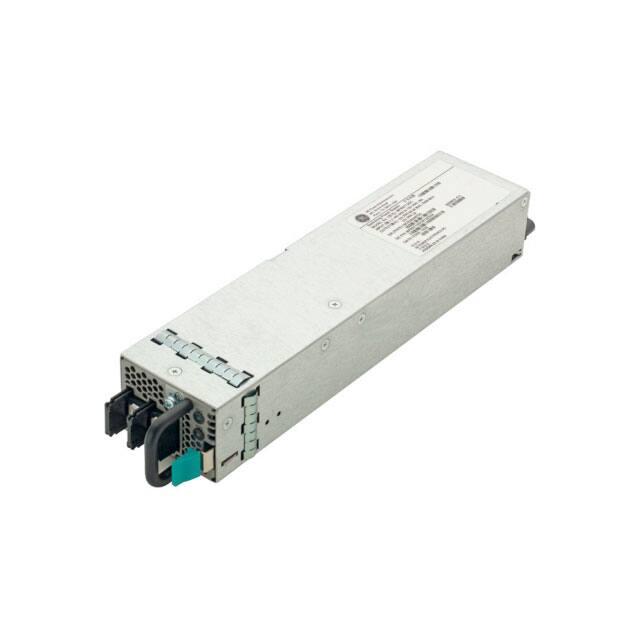
MPR0712DCR12Z02A Power Supply
Input: -44VDC to -72VDC; Output: +12VDC, 700W; Auxiliary Voltage 12VDC @ 2A
The MPR0712DC series provides high efficiency
isolated power from the DC input mains. The industry
standard PMBus® compliant I2C communications bus
offers a full range of control and monitoring capabilities.
The SMBAlert signal pin automatically alerts customers
of any state change within the power supply.
Application
•
12VDC distributed power architectures
•
Network Attached Storage
•
Mid-End Servers
•
Storage Area Networks
•
Blade Servers
•
Routers/Switches
•
Network Equipment
•
Enterprise Networks
•
Advanced workstations
Compliant to RoHS II EU “Directive 2011/65/E
•
12VDC secondary Regulation: ± 2.5%
(-Z versions)
•
Hardware recoverable latched 12VDC overvoltage
•
Compliant to REACH Directive (EC) No 1907/2006
•
Auto recoverable overload & over temperature
•
2.15” x 9.0” x 1.57”
•
Firmware adjustable overload set point of 12V output
•
Efficiency : 94% at 50% load
•
Operating temperature: -5°C to 50°C
•
12VDC Regulation: set point ±0.33%, overall ±1%
•
Digital status & control: PMBus® serial bus
•
Turn-On overshoot: within regulation
•
Conducted EMI: class A with 6dB margin
•
Active current share on 12V with OR’ing function
•
Meets EN6100 immunity and transient standards
•
Remote sense on the 12V main output
•
Safety: UL, CAN/CSA, IEC, TUV, IEC62368-1
•
Hot insertion/removal (hot plug)
Features
•
Page 1
© 2020 ABB. All rights reserved.
�Technical Specifications
Absolute Maximum Ratings
Stresses over the absolute maximum ratings can cause permanent damage to the device. These are absolute stress ratings only. Functional
operation of the device is not implied at these or any other conditions over those given in the operations sections of the data sheet. Exposure to
absolute maximum ratings for extended periods can adversely affect the device reliability.
Parameter
Input Voltage: Continuous
Operating Ambient Temperature
Storage Temperature
Device
Min
Max
Unit
VIN
-44
-72
VDC
700W, -44 to-72VDC. De-rating above 48
°C
TA
-5
50
TSTG
-40
85
°C
1000
VDC
I/O Isolation voltage (100% factory Hi-Pot tested)
1
1
for reverse model
Electrical Specifications
Unless otherwise indicated, specifications apply overall operating input voltage, resistive load, and temperature conditions
Parameter
Operational Range
Main Output Turn OFF
Main Output Turn ON
Hysteresis between turn OFF and turn ON
Efficiency (T =25°C, V = 12V) V = -53VDC, exc. fan
100% load
50% load
20% load
Maximum Input Current (VO= VO, set, IO=IO, max)
VIN=-53VDC
Cold Start Inrush Current (between 0 to 200mSec)
Startup Time during DC ramp up.
Note: Following a “turn off” of the 12V Main output (for any reason
whatsoever) the output shall not be allowed to “turn on” again for
1sec (even if all necessary operating conditions are met).
Holdup time (Vout≥ 10.8V, Tamb = 25°C, 700W)
VIN = -44 VDC to -72VDC
Early warning prior to output falling below 10.8VDC
Isolation Input/Output
Input/Frame
Output/Frame
12VDC MAIN OUTPUT
Output Power -44 to -72 VDC, Cout 500-4000uF
Overall regulation (setpoint, line, load, temperature)
Ripple and noise (20MHz bandwidth, 0.1uF ceramic+10uF tantalum
connected)
Turn-ON overshoot
Turn-ON delay
Remote ON/OFF delay time
Turn-ON rise time (10 – 90% of Vout)
Transient response 50% step [10%-50%, 50% - 100%] (dI/dt – 1A/µs, recovery
1ms)
Page 2
© 2020 ABB. All rights reserved.
Device
Min
Typ
Max
Unit
VIN
V
V
V
-44
-37
-42
-53
-38
-43
5
-72
-39
-44
VDc
VDC
VDC
VDC
92.0
94.0
90.0
IIN
14.7
IIN
T
T
%
ADC
25
APEAK
3
Sec
2
1
1000
1000
500
ms
0
VDC
VDC
VDC
Max
Unit
700
+2
W
%
V0
1201
mVP-P
V0
V0
T
T
+3
2
150
80
%
sec
ms
ms
+5
%V0
Symbol
Min
W
V0
0
-2
T
-5
Typ
�Technical Specifications
Electrical Specifications
Parameter
Device
Min
Typ
Max
Unit
Overvoltage protection, latched
(recovery by cycling off/on via hardware or PMBus® )
T
13.0
13.8
14.5
Overvoltage
protection,
latched
Output current -44 ≤VIN ≤ -72
V
0
58.3
ADC
Current limit, the output shall shutdown when an overcurrent condition is
detected.
It will auto restart after 1sec; however, if the overcurrent condition is
redetected the output will once again shutdown. The output will once again
re-start, however if the overcurrent condition persists it will latch of after the
fifth unsuccessful attempt.
To reset the latch, it will be necessary to toggle the PS_ON_L
signal (B4) or recycle the incoming AC source.
I0
60
70
ADC
Hot Swap Transients
I0
-5
+5
%
Active current share
I0
-5
+5
% of FL
STANDBY OUTPUT
Parameter
Device
Min
Set point
Overall regulation (setpoint, line, load, temperature)
VO
Ripple and noise (20MHz bandwidth, 0.1uF ceramic+10uF tantalum connected)
VO
Output current
Transient response 50% step [10%-50%, 50% - 100%] (dI/dt – 1A/µs, recovery
500µs)
Overvoltage protection, latched
Overload protection The output shall shutdown when an overcurrent is detected.
It will auto restart after 2sec; however, if the overcurrent is re- detected the
output will once again shutdown.
This cycle will occur indefinitely while the overcurrent condition
Note: Standby output voltage allowed to dip to 10.0V temporarily during fault
conditions on the main output (e.g., a short circuit or remote off the main output
pins or turn off main and standby with heavy load)
Page 3
© 2020 ABB. All rights reserved.
Typ
Max
12.0
11.7
(see note below)
Unit
VDC
12.3
VDC
120
0
2
ADC
13
14.5
VDC
IO
2.5
ADC
�Technical Specifications
General Specifications
Parameter
Device
Symbol
Typ
Unit
Calculated Reliability Per Telcordia SR-332 M1C1 @40°C
Weight
1.67
Lbs
EMC Compliance
Parameter
Criteria
Standard
Conducted emissions
EN55022, FCC Docket
20780 part 15, subpart J
Radiated emissions1
EN55022
A
Voltage dips
----
criteria A
-53Vin, 80% load, Dip 100% Duration 4ms
DC
Level
Test
A with
0.15 – 30MHz
30 – 1000MHz
Voltage surge
EN61000-4-5
1kV
Common and differential mode, unit passes
criteria A (normal performance)
Fast transients
EN61000-4-4
Level 3, criteria A
5/50ns, 2kV (common mode)
Conducted RF fields
EN61000-4-6
Level 3, criteria A
140dBµV, 0.15-80MHz, 80% AM
Radiated RF fields
EN61000-4-3
Level 3, criteria B
10V/m, 80-1000MHz, 80% AM
EN61000-4-2
Level 4, criteria A
8kV contact, 15kV air
IEC/EN 61000-4-8
Level 2, criteria B
3A/m
Enclosure immunity
ESD
Magnetic Field
Environmental Specifications
Parameter
Device
Min
Ambient Inlet Temperature Rating
Reverse airflow (air enters rear connector, exhausts at handle). 44-72VDC,
700W. De-rating above 48C (see following chart).
TA, Reverse
-5
Ambient Temperature Short Term≤96hrs event, and ≤96hrs total/year, which
can exceed IPC9592 derating, but OTP and mfgr’s max temp specs must apply
reverse airflow. De-rating above 40C allowed.
TA, Reverse
-10
55
-40
70
Storage Temperature
Typ
o
Operating Altitude Design Requirement without derating at 40 C inlet
Acoustic noise (full load)
Max
Unit
oC
3000
57
m
dBA
Over Temperature Protection (inlet)
Auto restart with 4°C hysteresis for recovery (warning issued at 70°C)
Humidity Relative humidity, non-condensing
Operating, +45C
Storage
Operational Vibration
IPC6592 2.4G
Non-Operating Shock
30
Grms
Safety Specifications
Applicable Standard
IEC 62368-1
Audio/video, information and communication technology equipment – Part 1: Safety requirements
UL 62368-1
Safety of information technology equipment, including electrical business equipment
CAN/CSA-C22.2 No. 62368-1
Audio/video, information and communication technology equipment - Part 1: Safety requirements (BiNational standard, with UL 62368-1)
Page 4
© 2020 ABB. All rights reserved.
�Technical Specifications
Output Power Derating versus Ambient Inlet Temperature
Feature Specifications
Unless otherwise indicated, specifications apply overall operating input voltage, resistive load, and temperature conditions. See
Feature Descriptions for additional information.
Page 5
© 2020 ABB. All rights reserved.
�Technical Specifications
Status and Control signals
Signal Name
I/O
Description
INPUT_OK
(DC Source)
Output
PW_OK
(Output OK)
Output
SMB_ALERT
(FAULT/WARNING)
Output
(Power
Output
The signal is used to detect the presence (installed) of a PSU by the host
system. The signal is connected to PSU logic SGND within the power module.
Passive connection to +VSB_Return.
A logic low < 0.8VDC
Input
This signal is pulled up internally to the internal housekeeping supply(within
the power supply). The power supply main 12VDC output will be enabled
when this signal is pulled low to +VSB_Return.
In the low state the signal input shall not source more than 1mA of current.
The 12VDC output will be disabled when the input is
than 2.4V,
or open circuited. Cycling this signal shall clear latched fault conditions.
Pulled up internally via 10K to 3.3VDC.
A logic high >3.0VDC
A logic low < 0.8VDC
Input is via CMOS Schmitt trigger buffer.
PS_ON
PS_KILL
Input
ADDR
(Address Select)
Input
SCL (Serial Clock)
Both
SDA (Serial Data)
Both
V1_SENSE
V1SENSE_RTN
Input
ISHARE
BiDirectional
Analogue
Bus
Page 6
© 2020 ABB. All rights reserved.
The signal output is driven high when input source is available and within
acceptable limits. The output is driven low to indicate loss of input power.
Interface Details
Pulled up internally via 10K to 3.3VDC.
A logic high >3.0VDC
A logic low < 0.8VDC
Driven low by internal CMOS buffer.
Pulled up internally via 10K to 3.3VDC.
A logic high >3.0VDC
A logic low < 0.8VDC
Driven low by internal CMOS buffer.
The signal is asserted, driven high, by the power supply to indicate
output is valid. If main output failed, then this output will be hi-Z or driven
low. The output is driven low to indicate that the Main output is outside of
lower limit of regulation (3.0VDC
A logic low < 0.8VDC
Driven low by internal CMOS buffer.
Pulled up internally via 10K to 3.3VDC.
A logic high >3.0VDC
A logic low < 0.8VDC
Input is via CMOS Schmitt trigger buffer
DC voltage between the limits of 0 and
+3.3VDC.
VIL is 0.8V maximum
VOL is 0.4V maximum when sinking 3mA
VIH is 2.1V minimum
A serial data line compatible with PMBus® TPower Systems Management
VIL is 0.8V maximum
Protocol Part 1 – General Requirements Rev 1.2.
VOL is 0.4V maximum when sinking 5mA
The signal is provided with a series isolator device to disconnect the internal
VIH is 2.1V minimum
power supply bus if the power module is unpowered.
Remote sense connections intended to be connected at and sense the voltage at the point of load. The voltage sense will interact with the internal
module regulation loop to compensate for voltage drops due to connection
Compensation for a up to 0.12VDC total
resistance between the output connector and the load. If remote sense
connection drop (output and return concompensation is not required, then the voltage can be configured for local
nections).
sense by:
1. V1_SENSE directly connected to power blades 6 to 10 (inclusive)
2. V1_SENSE_RTN directly connected to power blades 1 to 5 (inclusive)
The current sharing signal is connected between sharing units (forming an ISHARE bus). It is an input and/or an
output (bi-directional analogue bus) as the voltage on the line controls the current share between
A power
supply will respond to a change in this voltage, but a power supply can also change the voltage depending on the load
drawn from it. On a single unit the voltage on the pin (and the common ISHARE bus would read 8.74VDC at 100% load
(module capability). For two identical units sharing the same 100% load this would read 4.37VDC for perfect current sharing (i.e. 50% module load capability per unit).
Analogue voltage: +10V maximum; 10K to +12V_RTN
�Technical Specifications
Digital Interface Specifications
PMBus® Signal Interface Characteristics
Parameter
Symbol
Min
Max
Unit
Input logic high voltage (CLK, DATA)
Conditions
VIH
0.7VDD
3.6
V
Input logic low voltage (CLK, DATA)
VIL
0
0.8
V
Input high sourced current (CLK, DATA)
IIH
0
10
μA
Output low sink voltage (CLK, DATA, SMBALERT#)
IO=5mA
Output low sink current (CLK, DATA, SMBALERT#)
VOL
IOL
Output high open drain leakage current (CLK, DATA, SMBALERT#)
PMBus® operating frequency range
0.4
V
5
mA
VO=3.6V
IOH
0
10
μA
Slave Mode
FPMB
10
400
kHz
25
ms
Measurement System Characteristics
Clock stretching
tstretch
IOUT measurement range
Linear
IOUT measurement accuracy 25°C
VOUT measurement range
Linear
VOUT measurement accuracy
Temp measurement range
Linear
Temp measurement accuracy1
IIN measurement range
Linear
IIN measurement accuracy
VIN measurement range
Linear
VIN measurement accuracy
PIN measurement range
Linear
PIN measurement accuracy
Fan Speed measurement range
IRNG
0
74
A
IOUT
-3
+3
% of FL
VOUT(rng)
0
14
V
VOUT(acc)
-5
+5
%
Temp(rng)
0
125
Temp(acc)
-5
+5
C
%
IIN(rng)
0
31
ADC
IIN(acc)
-5
+5
% of FL
VIN(rng)
0
88
VDC
VIN(acc)
-5
+5
% of FL
PN(rng)
0
1023
W
PIN(acc)
-5
+5
% of FL
Linear
Fan Speed measurement accuracy
Fan speed control range
number
0
30k
RPM
-10
10
%
0
100
%
Visual Indicators (LEDs)
Input (Green), Output (Bicolor Green/Amber)
Status Indicators
LED NAME
LED MODE
LED STATE/
OPERATION
DESCRIPTION
Input
OK
Solid Green
Input voltage operating within normal specified range
Input
OV/UV Warning
Blinking Green
Input voltage operating in: 1) overvoltage warning, 2) under voltage warning range, or 3) above
overvoltage range
Input
OFF or Fault
Off
Input voltage operating: 1) below under voltage range, or 2) not present
Output
Power Good
Solid Green
Main output & standby output enabled with no power supply warning or fault detected
Output
Standby
Blinking Green
Standby output enabled with no power supply warning or fault detected
Output
Warning
Blinking Amber
Power supply warning detected as per PMBus® STATUS_X reporting bytes*
Output
Fault
Solid Amber
Power supply fault detected as per PMBus® STATUS_X reporting
Output
OFF
Off
Input below under voltage range
* LED fault/warning operation follows PMBus fault/warning reporting status flags but will not be “sticky” (i.e., if the fault stimulus is removed, even though the actual fault/warning is still showing [still “sticky” and not cleared], the
relevant LED will revert to normal (non-fault) operation.
Page 7
© 2020 ABB. All rights reserved.
�Technical Specifications
Timing Specifications
Turn-on delay & output rise time
Time
Min (ms)
Max (ms)
Vsb Rise Time
20
60
V1 Rise Time
20
80
Vsb Power-on Delay
-
2000
V1 Power-on Delay
-
2000
V1 PS_ON Delay
150
V1 PW_OK Delay
100
300
INPUT_OK Detect
300
1000
The turn-on delay after application of DC input within the operating range shall as defined in the following tables. The output rise times
shall be measured from 10% of the nominal outputs to the lower limit of the regulation band as defined in the following tables.
Power removal holdup, fall time and signaling
Power Removal Timing
Min
Vsb holdup with remote off
40ms
V1 holdup
Total
-
Typ
Max
2ms
Input fail detect
3ms
PW_OK delay off
1ms
PW_OK Hold up
-
1ms
Notes
700W
-
700W, 53VDC
-
700W
-
700W
Turn-off (Shutdown by PS_ON)
Turn-off Timing
Page 8
© 2020 ABB. All rights reserved.
Min
Max
Notes
Must be monotonic
V1 Fall time
-
-
V1 PS_OFF delay
-
6ms
PW_OK delay off
1ms
�Technical Specifications
Design Features
9th ACK bit, the exception being the START command.
Serial Bus Communications
The I²C interface facilitates the monitoring and control of various operating
parameters within the unit and transmits these on demand over an
industry standard I²C Serial bus.
All signals are referenced to ‘SGND’.
Pull-up resistors: The clock, data, and SMBAlert lines do not have any
internal pull-up resistors inside the rectifier. The customer is responsible for
ensuring that the transmission impedance of the communications lines
complies with I2C and SMBus standards.
Serial Clock (SCL): The clock pulses on this line are generated by the host
that initiates communications across the I²C Serial bus. This signal needs to
be pulled HI externally through a resistor as necessary to ensure that rise
and fall time timing and the maximum sink current complies to the I²C /
SMBus specifications.
Serial Data (SDA): This line is a bi-directional data line. This signal needs to
be pulled HI externally through a resistor as necessary to ensure that rise
and fall time timing and the maximum sink current complies to the I²C /
SMBus specifications.
Digital Feature Descriptions
PMBus® compliance: The rectifier is fully compliant to the Power
Management Bus (PMBus®) rev1.2 requirements. This Specification can be
obtained from www.pmbus.org.
‘Manufacturer Specific’ commands are used to support additional
instructions that are not in the PMBus™ specification.
All communication over the PMBus interface must support the Packet Error
Checking (PEC) scheme. The PMBus master must generate the correct PEC
byte for all transactions, and check the PEC byte returned by the rectifier.
Non-volatile memory is used to store configuration settings. Not all settings
programmed into the device are automatically saved into this non-volatile
memory. Only those specifically identified as capable of being stored can be
saved. (see the Table of Commands for which command parameters can be
saved to non-volatile storage).
Non-supported commands: Non supported commands are flagged by
setting the appropriate STATUS bit and issuing a SMBAlert to the ‘host’
controller.
I²C Bus Lock-Up detection: The device will abort any transaction and drop off
the bus if it detects the bus being held low for more than 35ms.
Communications speed: Both 100kHz and 400kHz clock rates are supported.
The rectifiers default to the 100kHz clock rate.
Packet Error Checking (PEC): The rectifier will not respond to commands
without the trailing PEC. The integrity of communications is compromised if
packet error correction is not employed. There are many functional features,
including turning off the main output, that require validation to ensure that the
desired command is executed.
PEC is a CRC-8 error-checking byte, based on the polynomial C(x) = x8 + x2 + x +
1, in compliance with PMBus™ requirements. The calculation is based in all
message bytes, including the originating write address and command bytes
preceding read instructions. The PEC is appended to the message by the device
that supplied the last byte.
SMBAlert: The μC driven SMBAlert signal informs the ‘master/host’ controller
that either a STATE or ALARM change has occurred. Normally this signal is HI.
The signal will change to its LO level if the rectifier has changed states and the
signal will be latched LO until the rectifier receives a ‘clear_faults’ instruction.
The signal will be triggered for any state change, including the following
conditions:
•
•
•
•
•
•
If a non-supported read is requested the rectifier will return 0x00h for data.
•
Data out-of-range: The rectifier validates data settings and sets the data
out-of-range bit and SMBAlert if the data is not within acceptable range.
•
Master/Slave: The ‘host controller’ is always the MASTER. Rectifiers are always
SLAVES. SLAVES cannot initiate communications or toggle the Clock. SLAVES
also must respond expeditiously at the command of the MASTER as required by
the clock pulses generated by the MASTER.
Clock stretching: The ‘slave’ μController inside the rectifier may initiate clock
stretching if it is busy and it desires to delay the initiation of any further
communications. During the clock stretch the ‘slave’ may keep the clock LO
until it is ready to receive further instructions from the host controller.
The maximum clock stretch interval is 25ms.
The host controller needs to recognize this clock stretching, and refrain from
issuing the next clock signal, until the clock line is released, or it needs to delay
the next clock pulse beyond the clock stretch interval of the rectifier. Note that
clock stretching can only be performed after completion of transmission of the
Page 9
© 2020 ABB. All rights reserved.
VIN under or over voltage
VOUT under or over voltage
IOUT over current
Over Temperature warning or fault
Fan Failure
Communication error
PEC error
Invalid command
SMBAlert is asserted during power up to notify the master that a new rectifier
has been added to the bus.
The rectifier will clear the SMBAlert signal (release the signal to its HI state)
upon the following events:
•
•
Receiving a CLEAR_FAULTS command
Bias power to the processor is recycled
The rectifier will re-assert the Alert line if the internal state of the rectifier has
changed, even if that information cannot be reported by the status registers
until a clear_faults is issued by the host. If the Alert asserts, the host should
respond by issuing a clear_faults to retire the alert line (this action also
provides the ability to change the status registers). This action triggers another
Alert assertion because the status registers changed states to report the latest
state of the rectifier. The host is now able to read the latest reported status
register information and issue a clear_faults to retire the Alert signal.
�Technical Specifications
Re-initialization: The I2C code is programmed to re-initialize if no activity is
detected on the bus for 5 seconds. Reinitialization is designed to guarantee that
the I2C μController does not hang up the bus. Although this rate is longer than
the timing requirements specified in the SMBus specification, it had to be
extended in order to ensure that a re-initialization would not occur under
normal transmission rates. During the few μseconds required to accomplish
reinitialization the I2C μController may not recognize a command sent to it. (i.e.
a start condition).
Read back delay: The rectifier issues the SMBAlert notification as soon as the
first state change occurred. During an event a few different states can be
transitioned to before the final event occurs. If a read back is implemented
rapidly by the host a successive SMBAlert could be triggered by the
transitioning state of the rectifier. In order to avoid successive SMBAlert s and
read back and also to avoid reading a transitioning state, it is prudent to wait
more than 2 seconds after the receipt of a SMBAlert before executing a read
back. This delay will ensure that only the final state of the rectifier is captured.
Successive read backs: Successive read backs to the rectifier should not be
attempted at intervals faster than every one second. This time interval is
sufficient for the internal processors to update their data base so that
successive reads provide fresh data.
1
S
Sr
1
S
Slave address
Low data byte
Wr
A
Slave Address
1
S
Slave address
Byte count = N
1
A
High data byte
1
A
PEC
A
1
P
Command Code
Rd
A
A
1
A
Wr
A
Data 1
……….
Command Code
A
Data 2
A
Data N
Block read format:
1
S
Slave address
Sr
……….
1
A
Wr
Slave Address
Byte count = N
Command Code
A
Block write format:
PMBus® Commands
Standard instruction: Up to two bytes of data may follow an instruction
depending on the required data content. Analog data is always transmitted as
LSB followed by MSB. PEC is mandatory and includes the address and data
fields.
Wr
Block
communications: When writing or reading more than two bytes of data at a time
BLOCK instruction for WRITE and READ commands are used instead of the
Standard Instructions above to write or read any number of bytes greater than
two.
Global Broadcast: This is a powerful command because it instructs all rectifiers
to respond simultaneously. A read instruction should never be accessed
globally. The rectifier should issue an ‘invalid command’ state if a ‘read’ is
attempted globally.
For example, changing the ‘system’ output voltage requires the global
broadcast so that all paralleled rectifiers change their output simultaneously.
This command can also turn OFF the ‘main’ output or turn ON the ‘main’
output of all rectifiers simultaneously. Unfortunately, this command does have
a side effect. Only a single rectifier needs to pull down the ninth acknowledge
bit. To be certain that each rectifier responded to the global instruction, a READ
instruction should be executed to each rectifier to verify that the command
properly executed. The GLOBAL BROADCAST command should only be
executed for write instructions to slave devices.
Slave address
A
A
Rd
Command Code
A
Data 1
Data N
A
Data 2
A
A
NA
Linear Data Format: The definition is identical to Part II of the PMBus
Specification. All standard PMBus values, except for output voltage related
functions, are represented by the linear format described below. Output
voltage functions are represented by a 16-bit mantissa. Output voltage has an
E=-9 constant exponent.
The Linear Data Format is a two-byte value with an 11-bit, two’s complement
mantissa and a 5-bit, two’s complement exponent or scaling factor, its format is
shown below.
The relationship between the Mantissa, Exponent, and Actual
Master to Slave
Slave to Master
SMBUS annotations; S – Start , Wr – Write, Sr – re-Start, Rd – Read,
A – Acknowledge, NA – not-acknowledged, P – Stop
Bit
7
Data Byte High
6 5 4 3
Exponent (E)
2
1
0
7
Data Byte Low
6 5 4 3 2
Mantissa
1
Value (V) is given by the following equation:
Standard READ: Up to two bytes of data may follow a READ request depending
on the required data content. Analog data is always transmitted as LSB followed
by MSB. PEC is mandatory and includes the address and data fields.
Page 10
© 2020 ABB. All rights reserved.
V = M * 2E
Where: V is the value, M is the 11-bit, two’s complement mantissa, E is the
5-bit, two’s complement exponent
0
�Technical Specifications
Standard features
Supported features that are not readable: The commands below are
supported at the described setting, but they cannot be read back through the
command set.
Status and Alarm registers: The registers are updated with the latest
operational state of the rectifier. For example, whether the output is ON or OFF
is continuously updated with the latest state of the rectifier. However, alarm
information is maintained until a clear_fault command is received from the
host. For example, the shutdown or OC_fault bits stay in their alarmed state
until the host clears the registers.
A clear_faults clears all registers. If a fault persists after the clear_faults is
commanded, the register bit annunciating the fault is reset again.
Command
Comments
ON_OFF_CONFIG (0x02)
Both the CNTL pin, and the OPERATION
command, enabling or disabling the
output, are supported. Other options are
not supported.
400KHz, ALERT#
1.2
Capability (0x19)
PMBus revision (0x98)
PMBus® Addressing
Hardware setting: The signal pin, ADDR(A3) configure the address of the power
supply. Note that the ground reference for addressing is Signal Ground (SGND).
Internally each power supply has a 10kΩ pull up resistor between the ADDR pin
and 3.3V. The resistance between the ADDR pin and SGND shall determine the
values for A2-A0. The nominal resistor and corresponding voltage value for
each position is tabulated below.
Address
ADDR PIN (A3) resistor to
GND (K-ohm)
Nominal
voltage(V)
A2
A1
A0
0.82
2.7
5.6
8.2
15
27
56
180
0.25
0.70
1.18
1.48
1.98
2.41
2.80
3.12
0
0
0
0
1
1
1
1
0
0
1
1
0
0
1
1
0
1
0
1
0
1
0
1
Firmware setting:
Device
Address
µP
Broadcast
EEprom
B0 – BF
Address Bit Assignments
(Most to Least Significant)
3
2
1
1
A2
A1
A0
0
0
A2
A1
A0
A0 – AF
MSB
PMBus® Command set:
Command
Operation
Clear_Faults
Write _Protect
Page 11
© 2020 ABB. All rights reserved.
Hex
Code
0x01
0x03
0x10
Yes/80
0
R/W
R/W
LSB
Restore_default_all
Restore_user_all
0x12
0x16
Store_user_code
Restore_user_code
Vout_mode
Vin_ON
Vin_OFF
Fan_config_1_2
Fan_command_1
Vout_OV_fault_limit
Vout_OV_fault_response
Vout_OV_warn_limit
Vout_UV_warn_limit
Vout_UV_fault_limit
Vout_UV_fault_response
Iout_OC_fault_limit
Iout_OC_fault_response
Iout_OC_LV_fault_limit
Iout_OC_warn_limit
OT_fault_limit
OT_fault_response
OT_warn_limit
Vin_OV_fault_limit
Vin_OV_fault_response
Vin_OV_warn_limit
Vin_UV_warn_limit
Vin_UV_fault_limit
Vin_UV_fault_response
Status_byte
Status_word (+ byte)
Status_Vout
Status_Iout
Status_Input
Status_temperature
Status_CML
Status_fans_1_2
Read_Vin
Read_Iin
Read_Vout
Read_Iout
Read_temp_primary
Read_temp_oring
Read_temp_sr
Read_fan_speed_1
Read_Pin
Mfr_ID
Mfr_model
Mfr_revision
Mfr_serial
Read_firmware_rev
Read_run_timer
Read_ temp_inlet
0x17
0x18
0x20
0x35
0x36
0x3A
0x3B
0x40
0x41
0x42
0x43
0x44
0x45
0x46
0x47
0x48
0x4A
0x4F
0x50
0x51
0x55
0x56
0x57
0x58
0x59
0x5A
0x78
0x79
0x7A
0x7B
0x7C
0x7D
0x7E
0x81
0x88
0x89
0x8B
0x8C
0x8D
0x8E
0x8F
0x90
0x97
0x99
0x9A
0x9B
0x9E
0xD5
0xD6
0xDB
Reserved for factory use
Reserved for factory use
Reserved for factory use
0XDC
0XDD
0XDE
Yes
No / 43
No / 38
Yes / 90
Yes / 14.0
No / 80
Yes / 13.5
Yes / 10.8
Yes / 10.0
No / C0
Yes / 66
No / F8
Yes / 7.0
Yes / 62.0
Yes / 130
Yes / C0
Yes / 120
No / 76
No / C0
Yes / 74
Yes / 40
No / 38
No / C0
16
16
�Technical Specifications
Command Descriptions
and is returned by this command.
Operation (0x01): Turns the 12V output ON or OFF. The default state is ON
at power up. Only the following data bytes are supported:
Vin_ON (0x35): This is a ‘read only’ register that informs the controller at
what input voltage level the rectifier turns ON.
The default value is tabulated in the data section.
FUNCTION
Unit ON
Unit OFF
DATA BYTE
Vin_OFF (0x36): This is a ‘read only’ register that informs the controller at
what input voltage level the rectifier turns OFF. The default value is tabulated in the data section.
To RESET the rectifier using this command, command the rectifier OFF, wait
at least 2 seconds, and then command the rectifier back ON. All alarms and
shutdowns are cleared during a restart.
Clear_faults (0x03): Clears all STATUS and FAULT registers and resets the
Alert# line of the I2C side in control. The I2C side not in control cannot clear
registers in the power supply. This command is always executable.
If a fault persists after the issuance of the clear_faults command, the
specific registers indicating the fault first clears
have their parameters read, regardless of the write_protect settings. The
contents of this register cannot be stored into non-volatile memory using
the Store_user_code may command. The but then get set again to indicate
that the unit is still in the fault state.
WRITE_PROTECT register (0x10): Used to control writing to the PMBus
device. The intent of this command is to provide protection against
accidental changes. All supported commands default setting of this register
is enable_all_writes, write_protect 0x00h. The write_protect command
must always be accepted.
DATA BYTE
Enable all writes
Disable all writes except write_protect
Disable all writes except write_protect and
OPERATION
Restore_Default_All (0x12): Restores all operating register values and
responses to the factory default parameters set in the rectifier. The factory
default cannot be changed.
Fan_config_1_2 (0x3A): This command requires that the fan speed be commanded by duty cycle. Both fans must be commanded simultaneously. The
tachometer pulses per revolution is not used. Default is duty cycle control.
Fan_command_1 (0x3B): This command instructs the rectifier to increase
the speed of both fans. The transmitted data byte represents the hex
equivalent of duty cycle in percentage, i.e. 100% = 0 x 64h. The command
can only increase fan speed, it cannot instruct the rectifier to reduce the fan
speed below what the rectifier requires for internal control. An
incorrect
value will result in a ‘data error’.
Sending 00h tells the rectifier to revert back to its internal control.
Vout_OV_fault_limit (0x40): Sets the value at which the main output voltage will shut down. The default OV_fault value is set at 14.0Vdc. This level
can be permanently changed and stored in non-volatile memory.
Vout_OV_fault_response (0x41): This is a ‘read only’ register. The only
allowable state is a latched.
Vout_OV_warn_limit (0x42): Sets the value at which a warning will be
issued that the output voltage is too high. The default OV_warn limit is set
at 13.5Vdc. Exceeding the warning value will set the Alert# signal. This level
can be permanently changed and stored in non-volatile memory.
Vout_UV_warn_limit (0x43): Sets the value at which a warning will be
issued that the output voltage is too low. The default UV_warning limit is
set at 10.8Vdc. Reduction below the warning value will set the Alert# signal.
This level can be permanently changed and stored in non-volatile memory.
Restore_default_code (0x14): Restore only a specific register parameter
into the operating register section of the rectifier.
Vout_UV_fault_limit (0x44): Sets the value at which the rectifier will shut
down if the output gets below this level. The default UV_fault limit is set at
10Vdc. This register is masked if the UV is caused by interruption of the
input voltage to the rectifier. This level can be permanently changed and
stored in non-volatile memory.
Store_user_code (0x17): Changes the user default setting of a single
register. In this fashion some protection is offered to
Vout_UV_fault_response (0x45): This is a ‘read only’ register. The only
allowable state is restart.
ensure that only those registers that are desired to be changed are in fact
changed.
Iout_OC_fault_limit (0x46): Sets the value at which the rectifier will shut
down at High/Low Line. This level can be permanently changed and stored
in non-volatile memory.
Restore_user_code (0x18): Restores the user default setting of a single
register.
Vout_mode (0x20): This is a ‘read only’ register. The upper three bits
specify the supported data format, in this case Linear mode. The lower five
bits specify the exponent of the data in two’s complement binary format
for output voltage related commands, such as Vout_command. These
commands have a 16 bit mantissa. The exponent is fixed by the rectifier
Mode
Linear
Bits [7:5]
Page 12
© 2020 ABB. All rights reserved.
Bits [4:0] (Parameter)
Iout_OC_fault_response (0x47): This is a ‘read only’ register. The only allowable state is restart.
Iout_OC_warn_limit (0x4A): Sets the value at which the rectifier issues a
warning that the output current is getting too close to the shutdown level at
high/low line. This level can be permanently changed and stored in nonvolatile memory.
OT_fault_limit (0x4F): Sets the value at which the rectifier responds to an
OT event, sensed by the hottest sensor. The response is defined by the
OT_fault_response register.
�Technical Specifications
OT_fault_response (0x50): Sets the response if the output
overtemperature exceeds the OT_Fault_limit value. The default
OT_fault_response is hiccup (0xC0). The only two allowable states are
latched (0x80) or hiccup. The default response state can be permanently
changed and stored in non-volatile memory.
STATUS_VOUT (0X7A): Returns one byte of information of output voltage
related faults.
OT_warn_limit (0x51): Sets the value at which the rectifier issues a warning
when the hottest temperature sensor exceeds the warn limit.
Vin_OV_fault_limit (0x55): Sets the value at which the rectifier shuts down
because the input voltage exceeds the allowable operational limit. The
default Vin_OV_fault_limit is set at 76Vdc. This level can be permanently
lowered and stored in non- volatile memory.
STATUS_IOUT (0X7B): Returns one byte of information of output current
related faults. The OC Fault limit sets where current limit is set. The rectifier
shuts down below the LV fault limit setting.
Vin_OV_fault_response (0x56): This is a ‘read only’ register. The only
allowable state is restart.
Vin_OV_warn_limit (0x57): Sets the value at which a warning will be issued
that the input voltage is too high. The default OV_warn_limit is 74Vdc. This
level can be permanently changed and stored in non-volatile memory.
Vin_UV_warn_limit (0x58): This is another warning flag indicating that the
input voltage is decreasing dangerously close to the low input voltage
shutdown level. The default UV_fault_limit is 40Vdc. This level can be
permanently raised, but not lowered, and stored in non-volatile memory.
STATUS_INPUT (0X7C): Returns one byte of information of input voltage
related faults.
Vin_UV_fault_limit (0x59): Sets the value at which the rectifier shuts down
because the input voltage falls below the allowable operational limit. The
default Vin_UV_fault_limit is set at 38Vdc. This level can be permanently
raised and stored in non-volatile memory.
Vin_UV_fault_response (0x5A): This is a ‘read only’ register. The only
allowable state is restart.
STATUS_BYTE (0x78): Returns one byte of information with a summary of
the most critical device faults.
STATUS_TEMPERATURE (0x7D): Returns one byte of information of
temperature related faults.
STATUS_CML (0X7E): Returns one byte of information of communication
related faults.
TATUS_WORD (0x79): Returns status_byte as the low byte and the
following high_byte.
STATUS_fans_1_2 (0X81): Returns one byte of information of fan status.
Page 13
© 2020 ABB. All rights reserved.
�Technical Specifications
Read back Descriptions
Single parameter read back: Functions can be read back one at a time using
the read_word_protocol with PEC. A command is first sent out notifying the
slave what function is to be read back followed by the data transfer.
Analog data is always transmitted LSB followed by MSB. A NA following the
PEC byte signifies that the transmission is complete and is being terminated
by the
‘host’.
Slave address
Wr
Command Code
Read data field sends back in hex format the number of data bytes,
exclusive of the PEC number, that follows. Analog data is always
transmitted LSB followed by MSB. A No-ack following the PEC byte signifies
that the transmission is complete and is being terminated by the ‘host’.
Read_firmware_rev [0xD5]: Reads back the firmware revision of all three
µC in the rectifier.
Slave address
Sr
Sr
Slave address
Wr
Command Code 0xDD
Slave Address
Rd
Primary minor rev
1
A
Secondary minor rev
1
A
Primary major rev
MSB
A
PEC
No-Ack
P
i2c major rev
Read_fan_speed 1 (0x90): Reading the fan speed is in Linear Mode
returning the RPM value of the fan.
Read_FRU_ID (0x99, 0x9A, 0x9B, 0x9E): Returns FRU information. Must be
executed one register at a time.
Slave address
Wr
Command 0x9x
1
A
Secondary major rev
Read back error: If the µC does not have sufficient time to retrieve the
requested data, it has the option to return all FF’s instead of incorrect data.
1
A
i2c revision
Slave address
Byte_1
A
Byte
Rd
A
A
Byte_x
Byte count = x
A
PEC
No-Ack
Slave address
A
1
P
Mfr_ID (0x99): Manufacturer in ASCII – 6 characters maximum, General
Electric – Critical Power represented as, GE-CP
Mfr_ID (0x9A): Manufacturer model-number in ASCII – 16 characters, for
this unit: MPR0712DCxxxxxx
1
1
A PEC No-ack P
Read_run_timer [0xD6]: This command reads back the recorded
operational ON state of the rectifier in hours. The operational ON state is
accumulated from the time the rectifier is initially programmed at the
factory. The rectifier is in the operational ON state both when in standby
and when it delivers main output power. Recorded capacity is
approximately 10 years of operational state.
1
Sr
Byte Count = 6
Rd
Sr
Wr
Slave Address
Time - LSB
PEC
A
No-ack
Rd
Time
1
A
Command Code 0xDE
A
Byte count = 3
A
A
A
Time - MSB
A
1
P
Mfr_revision (0x9B): Total 7 bytes, provides the product series number
when the product was manufactured.
General performance descriptions
Mfr_serial (0x9E): Product serial number includes the manufacturing date,
manufacturing location in up to 16 characters. For example:
Default state: Rectifiers are programmed in the default state to
automatically restart after a shutdown has occurred. The default state can
be reconfigured by changing non-volatile memory (Store_user_code).
13KZ51018193xxx, is decoded as;
13 – year of manufacture, 2013
Restart after a latchoff: PMBus™ fault_response commands can be
configured to direct the rectifier to remain latched off for over_voltage,
over_temperature and over_current.
KZ – manufacturing location, in this case Matamoros
To restart after a latch off either of five restart mechanisms are available.
51 – week of manufacture
1. The hardware pin ON/OFF may be cycled OFF and then ON.
018193xxx – serial #, mfr choice
2. The unit may be commanded to restart via i2c through the Operation
command by cycling the output OFF followed by ON.
Manufacturer-Specific PMBus® Commands
3. Remove and reinsert the unit.
Many of the manufacturer-specific commands read back more than two
bytes. If more than two bytes of data are returned, the standard SMBus®
Block read is utilized. In this process, the Master issues a Write command
followed by the data transfer from the rectifier. The first byte of the Block
Page 14
© 2020 ABB. All rights reserved.
4. Turn OFF and then turn ON AC power to the unit.
5. Changing firmware from latch off to restart.
Each of these commands must keep the rectifier in the OFF state for at
least 2 seconds, except for changing to restart.
�Technical Specifications
A power system that is comprised of a number of rectifiers could have difficulty
restarting after a shutdown event because of the non-synchronized behavior of the
individual rectifiers. Implementing the latch-off mechanism permits a synchronized
restart that guarantees the simultaneous restart of the entire system.
A synchronous restart can be implemented by;
1. Issuing a GLOBAL OFF and then ON command to all rectifiers,
2. Toggling Off and then ON the ON/OFF (ENABLE) signal
3. Removing and reapplying input commercial power to the entire system.
The rectifiers should be turned OFF for at least 20 – 30 seconds in order to
discharge all internal bias supplies and reset the soft start circuitry of the
individual rectifiers.
Auto_restart: Auto-restart is the default configuration for over-current and
over-temperature shutdowns. These features are configured by the
PMBus® fault_response commands
Wiring diagram for output
CURRENT SHARING NOTS
Main current sharing is achieved using active current share method details.
Current sharing can be achieved with or without the remote sense (V_SENSE) connected to the common load.
+VSB outputs can be tied together for redundancy but total combined output power must not exceed the related standby power. The +VSB output has an internal
ORING MOSFEET for additional redundancy/internal short protection.
The current sharing pin B5 is connected between sharing units (from an ISHARE bus). It is an input and/or an output (bi-directional analogue bus) as the voltage on the
line controls the current share between sharing units. A power supply will respond to a change in this voltage but a power supply can also change the voltage
depending on the load drawn from it. On a single unit, the voltage on the pin (and the common IHSARE bus would read 8.74VDC at 100% load. For two units sharing
the same load this would read 4.37VDC for perfect current sharing (i.e. 50% load per unit).
The load for both the main 12V and VSB rails at the initial startup shall not be allowed to exceed the capability of a single unit. The load can be increased after a delay
of 3sec (minimum), to allow all sharing units to achieve steady regulation.
Page 15
© 2020 ABB. All rights reserved.
�Technical Specifications
Mechanical Outline
Connector Pin Assignments
Input Connector: Terminal Block Dinkle DT-7C-B14W-02; mating connector: Ring Terminal suitable for M4, OD: 8MM
Output Connector: MiniPAK HDL, 25s10p, RA Plug TE CONNECTIVITY 1926736-3
Mating connector: TE Connectivity 1926736-5
Function
6,7,8,9,10
1,2,3,4,5
+12V_OUT
+12V_RTN
Function
+12V Main Output
+12V Main Output Return
Standby Output
Standby Output
Standby Output
I2C Serial Data Line
PS_ON_L
Remote Sense Return (-VE)
Remote Sense (+VE)
I2C Serial Clock Line
Remote On/Off (Enable/Disable)
Standby Output
SMB_ALERT
Alert signal to host system
+VSB_Return/SGND
+VSB_Return/SGND
Unused
Unused
Unused
Address
Standby Output
Standby Output Return / Signal Ground
Standby Output Return / Signal Ground
No End User Connection
No End User Connection
No End User Connection
Address
Unused
Input_OK
PS_KILL
ISHARE
PW_OK
Unused
PRESENT_L
No End User Connection
Input Source Present & "OK"
Power Supply "kill"; short pin
Current Share bus; short pin
Power “OK"; short pin
No End User Connection
Power Module Present; short pin
Unused
No End User Connection
Page 16
© 2020 ABB. All rights reserved.
V1_SENSE_R
V1_SENSE
�Technical Specifications
Ordering Information
Please contact your ABB Sales Representative for pricing, availability and optional features.
PRODUCT
OUTPUT
STANDBY
AIRFLOW
ORDERING PART NUMBER
MPR0712DCR12Z02A
700W, +12Vout DC Input front-end
with 12Vsbaux
12V @2A
Reverse (Back to Front)
MPR0712DCR12Z02A
Page 17
© 2020 ABB. All rights reserved.
�ABB
601 Shiloh Rd.
Plano, TX USA
Go.ABB/Industrial
We reserve the right to make technical changes or modify the contents of this document without prior notice. With regard to
purchase orders, the agreed particulars shall prevail. ABB does not
ac-cept any responsibility whatsoever for potential errors or
possible lack of information in this document.
We reserve all rights in this document and in the subject matter and illustrations contained therein. Any reproduction, disclosure to third parties or utilization of its contents – in whole or in parts – is forbidden without prior written
consent of ABB.
Copyright© 2020 ABB
All rights reserved
Page 18
© 2020 ABB. All rights reserved.
�